

Integrated Device Technology Inc IDT74FCT621ATSOB, IDT74FCT621TSOB, IDT74FCT621ATSO, IDT74FCT621ATPB, IDT74FCT621ATP Datasheet
...
IDT54/74FCT621T/AT
FAST CMOS OCTAL BUS TRANSCEIVER (OPEN DRAIN) MILITARY AND COMMERCIAL TEMPERATURE RANGES
FAST CMOS
IDT54/74FCT621T/AT
OCTAL BUS TRANSCEIVER
(OPEN DRAIN)
Integrated Device Technology, Inc.
FEATURES:
• Std. and A speed grades
• Low input and output leakage ≤1µA (max.)
• CMOS power levels
• True TTL input and output compatibility
– VOH = 3.3V (typ.)
– VOL = 0.3V (typ.)
• Power off disable outputs permit “live insertion”
• Meets or exceeds JEDEC standard 18 specifications
• Product available in Radiation Tolerant and Radiation
Enhanced versions
• Military product compliant to MIL-STD-883, Class B
and DESC listed (dual marked)
• Available in DIP, SOIC, CERPACK and LCC packages
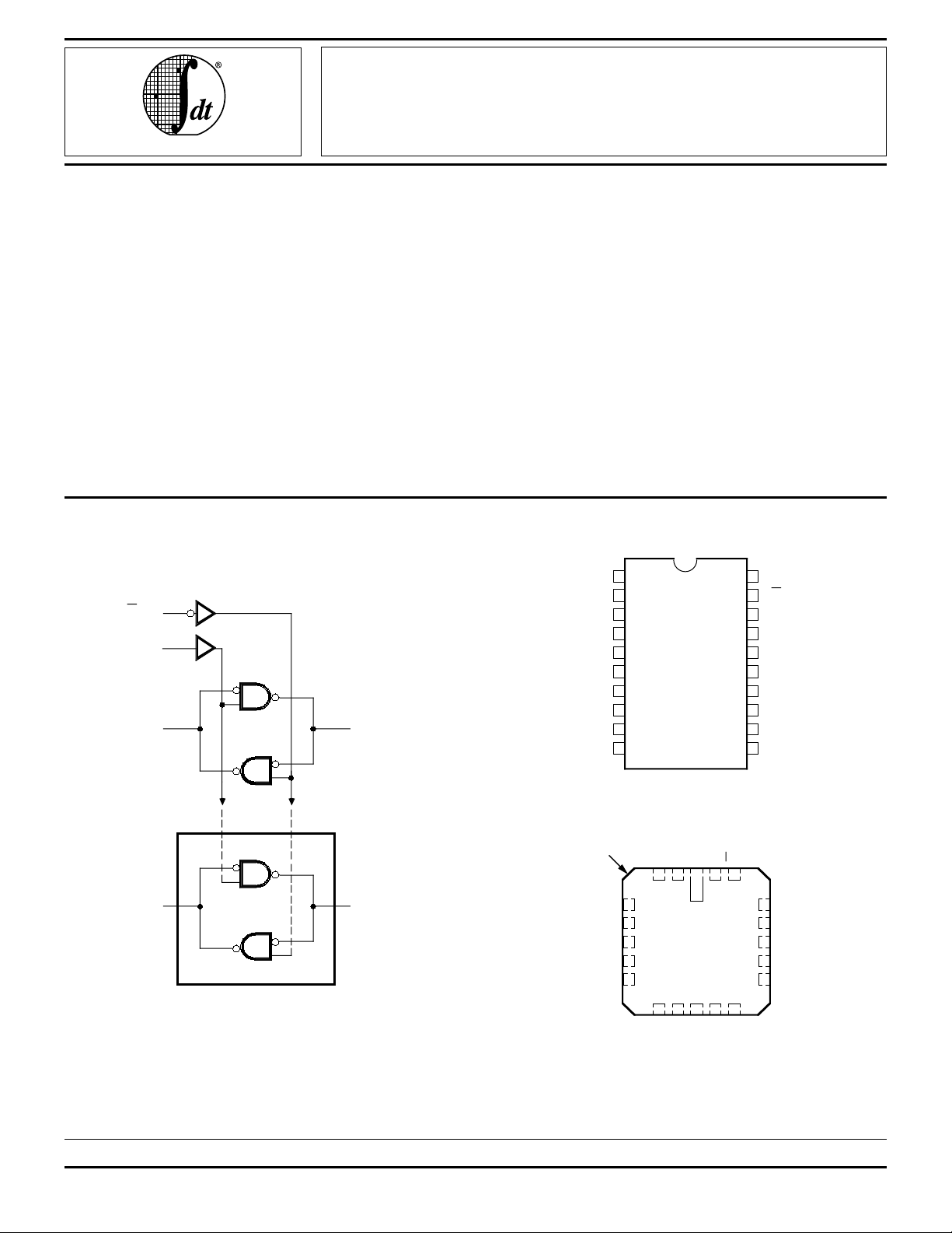
FUNCTIONAL BLOCK DIAGRAM
GBA
GAB
1
A
(1)
B
1
DESCRIPTION:
The IDT54/74FCT621T/AT is an octal transceiver with
non-inverting Open-Drain bus compatible outputs in both
send and receive directions. The B bus outputs are capable
of sinking 64mA providing very good capacitive drive
characteristics. These octal bus transceivers are designed for
asynchronous two-way communication between data buses.
The control function implementation allows for maximum
flexibility in timing.
PIN CONFIGURATIONS
GAB
A
A
A
A
A
A
A
A
GND
1
2
1
3
2
3
4
5
6
7
8
4
5
6
7
8
9
10
P20-1,
D20-1,
SO20-2
&
E20-1
DIP/SOIC/CERPACK
TOP VIEW
20
19
18
17
16
15
14
13
12
11
Vcc
GBA
B
1
B
2
B
3
B
4
B
5
B
6
B
7
B
8
2538 drw 02
2
32
4
5
6
7
8
10 11 12 13
9
8
A
A1A
GAB
1
L20-2
20 19
8
Vcc
GBA
18
17
16
15
14
B6B7B
B
1
B
2
B
3
B
4
B
5
2538 drw 03
A2–A
8
7 Other Transceivers
B
2–B8
2538 drw 01
INDEX
A
3
A
4
A
5
A
6
A
7
GND
LCC
TOP VIEW
The IDT logo is a registered trademark of Integreted Device Technology, Inc.
MILITARY AND COMMERCIAL TEMPERATURE RANGES APRIL 1994
1995 Integrated Device Technology, Inc. 6.18 DSC-4222/4
6.18 1
1
IDT54/74FCT621T/AT
FAST CMOS OCTAL BUS TRANSCEIVER (OPEN DRAIN) MILITARY AND COMMERCIAL TEMPERATURE RANGES
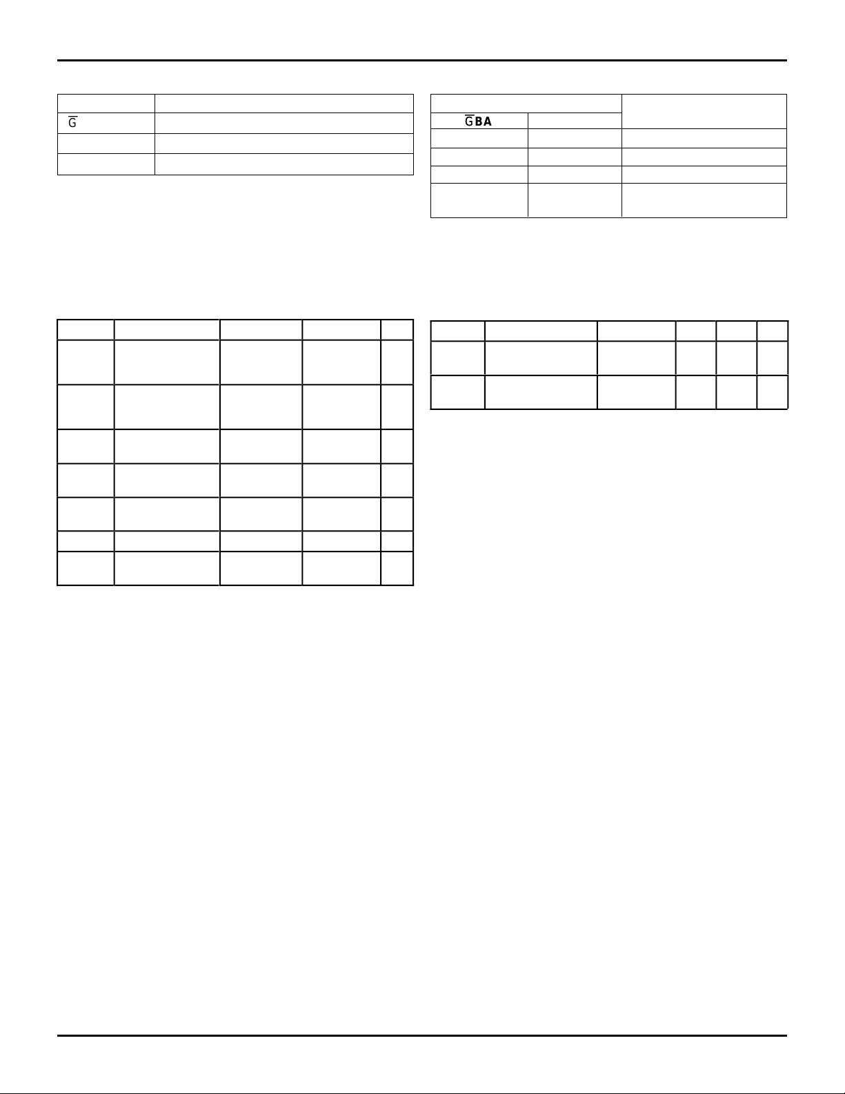
PIN DESCRIPTION
Pin Names Description
G
BA, GAB Enable Inputs
1 – A8 A Inputs or Open-drain Outputs
A
1 – B8 B Inputs or Open-drain Outputs
B
2538 tbl 01
ABSOLUTE MAXIMUM RATINGS
Symbol Rating Commercial Military Unit
(2)
VTERM
VTERM
TA Operating
TBIAS Temperature
TSTG Storage
PT Power Dissipation 0.5 0.5 W
IOUT DC Output
NOTES:
1. Stresses greater than those listed under ABSOLUTE MAXIMUM RATINGS may cause permanent damage to the device. This is a stress rating
only and functional operation of the device at these or any other conditions
above those indicated in the operational sections of this specification is
not implied. Exposure to absolute maximum rating conditions for
extended periods may affect reliability. No terminal voltage may exceed
V
2. Input and V
3. Outputs and I/O terminals only.
Terminal Voltage
–0.5 to +7.0 –0.5 to +7.0 V
with Respect to
GND
(3)
Terminal Voltage
with Respect to
GND
–0.5 to
V
0 to +70 –55 to +125 °C
Temperature
–55 to +125 –65 to +135 °C
Under Bias
–55 to +125 –65 to +150 °C
Temperature
–60 to +120 –60 to +120 mA
Current
CC by +0.5V unless otherwise noted.
CC terminals only.
CC +0.5
(1)
–0.5 to
VCC +0.5
V
2538 lnk 03
FUNCTION TABLE
(1)
Enable Inputs
GGBA GAB Function
L L B data to A bus
H H A data to B bus
H L OFF
L H B data to A bus
A data to B bus
NOTE: 2538 tbl 02
1. H = HIGH Voltage Level.
L = LOW Voltage Level.
OFF = HIGH if pull-up resistor is connected to Open-Drain output.
CAPACITANCE (TA = +25°C, f = 1.0MHz)
Symbol Parameter
CIN Input
Capacitance
COUT Output
Capacitance
NOTE:
1. This parameter is measured at characterization but not tested.
(1)
Conditions Typ. Max. Unit
VIN = 0V 6 10 pF
VOUT = 0V 8 12 pF
2538 lnk 04
6.18 2
 Loading...