

Integrated Device Technology Inc IDT74FCT574P, IDT74FCT574LB, IDT74FCT574L, IDT74FCT574EB, IDT74FCT574DB Datasheet
...
Integrated Device Technology, Inc.
FEATURES:
• IDT54/74FCT374/534/574 equivalent to FAST speed
and drive
• IDT54/74FCT374A/534A/574A up to 30% faster than
FAST
• IDT54/74FCT374C/534C/574C up to 50% faster than
FAST
•I
OL = 48mA (commercial) and 32mA (military)
• CMOS power levels (1mW typ. static)
• Edge triggered master/slave, D-type flip-flops
• Buffered common clock and buffered common threestate control
• Product available in Radiation Tolerant and Radiation
Enhanced versions
• Military product compliant to MIL-STD-883, Class B
• Meets or exceeds JEDEC Standard 18 specifications
DESCRIPTION:
The IDT54/74FCT374/A/C, IDT54/74FCT534/A/C and
IDT54/74FCT574/A/C are 8-bit registers built using an advanced dual metal CMOS technology. These registers consist
of eight D-type flip-flops with a buffered common clock and
buffered 3-state output control. When the output enable (OE)
is LOW, the eight outputs are enabled. When the OE input is
HIGH, the outputs are in the high-impedance state.
Input data meeting the set-up and hold time requirements
of the D inputs is transferred to the O outputs on the LOW-toHIGH transition of the clock input.
The IDT54/74FCT374/A/C and IDT54/74FCT574/A/ C have
non-inverting outputs with respect to the data at the D inputs.
The IDT54/74FCT534/A/C have inverting outputs.
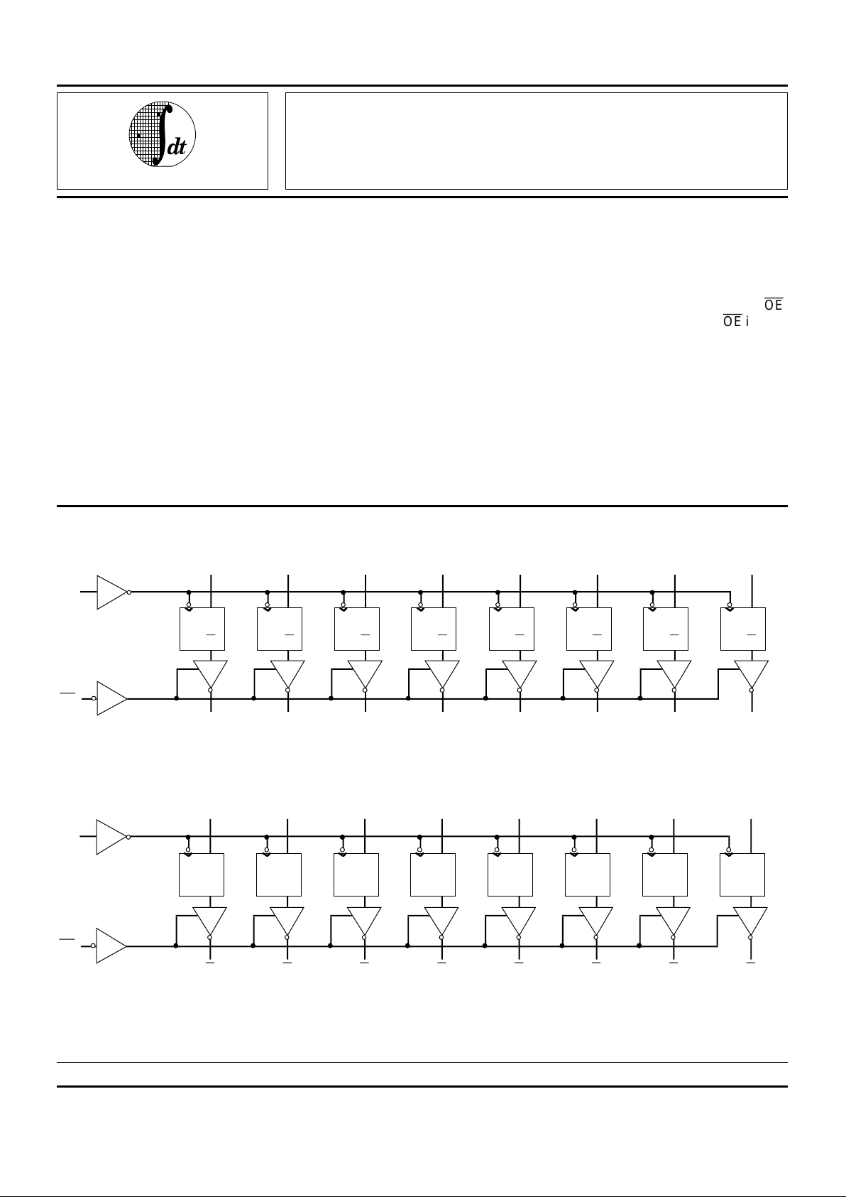
FUNCTIONAL BLOCK DIAGRAM IDT54/74FCT374 AND IDT54/74FCT574
D0
O0
D1
O1
D2
O2
D3
O3
D4
O4
D5
O5
D6
O6
D7
O7
CP
OE
D
Q
CP
D
Q
CP
D
Q
CP
D
Q
CP
D
Q
CP
D
Q
CP
D
Q
CP
D
Q
CP
FUNCTIONAL BLOCK DIAGRAM IDT54/74FCT534
D
0
O
0
D
1
O
1
D
2
O
2
D
3
O
3
D
4
O
4
D
5
O
5
D
6
O
6
D
7
O
7
CP
OE
D
Q
CP
D
Q
CP
D
Q
CP
D
Q
CP
D
Q
CP
D
Q
CP
D
Q
CP
D
Q
CP
The IDT logo is a registered trademark of Integrated Device Technology, Inc.
FAST is a trademark of National Semiconductor, Inc.
2603 cnv* 01
2603 cnv* 02
IDT54/74FCT374/A/C
IDT54/74FCT534/A/C
IDT54/74FCT574/A/C
FAST CMOS OCTAL D
REGISTERS (3-STATE)
MILITARY AND COMMERCIAL TEMPERATURE RANGES MAY 1992
1992 Integrated Device Technology, Inc. 7.13 DSC-4622/2
1

7.13 2
IDT54/74FCT374/534/574/A/C
FAST CMOS OCTAL D REGISTERS (3-STATE) MILITARY AND COMMERCIAL TEMPERATURE RANGES
OE
O
0
D
0
D
1
O
1
O
2
D
2
D
3
O
3
GND
O
7
D
7
D
6
O
6
O
5
D
4
CP
D
5
O
4
V
CC
1
2
3
4
5
6
7
8
9
10 11
12
13
14
15
16
17
18
19
20
DIP/SOIC/CERPACK
TOP VIEW
P20-1
D20-1
SO20-2
&
E20-1
IDT54/74FCT534
2603 cnv* 03 2603 cnv* 04
INDEX
D
1
O
1
O
2
D
2
D
3
D
7
D
6
O
6
O
5
D
5
O
0
D
0
OE
V
CC
O
7
O
3
GND
CP
O
4
D
4
LCC
TOP VIEW
3 2 20 19
1
4
5
6
7
8
18
17
16
15
14
9 10111213
L20-2
2603 cnv* 05 2603 cnv* 06
2603 cnv* 07 2603 cnv* 08
PIN CONFIGURATIONS
IDT54/74FCT374
IDT54/74FCT574
OE
D
0
D
1
D
2
D
3
D
4
D
5
D
6
D
7
GND
O
0
O
1
O
2
O
3
O
4
O
6
CP
O
5
O
7
V
CC
1
2
3
4
5
6
7
8
9
10 11
12
13
14
15
16
17
18
19
20
DIP/SOIC/CERPACK
TOP VIEW
P20-1
D20-1
SO20-2
&
E20-1
OE
O
0
D
0
D
1
O
1
O
2
D
2
D
3
O
3
GND
O
7
D
7
D
6
O
6
O
5
D
4
CP
D
5
O
4
V
CC
1
2
3
4
5
6
7
8
9
10 11
12
13
14
15
16
17
18
19
20
DIP/SOIC/CERPACK
TOP VIEW
P20-1
D20-1
SO20-2
&
E20-1
INDEX
D
2
D
3
D
4
D
5
D
6
O
1
O
2
O
3
O
4
O
5
D0
D1
OE
V
CC
O0
D7
GND
CP
O
7
O6
LCC
TOP VIEW
32 21
1
4
5
6
7
8
1
1
1
1
1
91111
L20-2
INDEX
D1 D7
O0
D0
OE
V
CC
O7
GND
LCC
TOP VIEW
D
6
O6
O5
D5
O1
O2
D2
D3
O4
D4
O3
3 2 20 19
1
4
5
6
7
8
18
17
16
15
14
9 10111213
L20-2
CP

IDT54/74FCT374/534/574/A/C
FAST CMOS OCTAL D REGISTERS (3-STATE) MILITARY AND COMMERCIAL TEMPERATURE RANGES
7.13 3
PIN DESCRIPTION
2603 tbl 06
FUNCTION TABLE
(1)
NOTE: 2603 tbl 05
1. H = HIGH Voltage Level Z = High Impedance
L = LOW Voltage Level NC = No Change
X = Don’t Care
ABSOLUTE MAXIMUM RATINGS
(1)
CAPACITANCE (TA = +25°C, f = 1.0MHz)
NOTES: 2603 tbl 01
1. Stresses greater than those listed under ABSOLUTE MAXIMUM
RATINGS may cause permanent damage to the device. This is a stress
rating only and functional operation of the device at these or any other
conditions above those indicated in the operational sections of this
specification is not implied. Exposure to absolute maximum rating conditions for extended periods may affect reliability. No terminal voltage may
exceed V
CC by +0.5V unless otherwise noted.
2. Input and V
CC terminals only.
3. Outputs and I/O terminals only.
Symbol Parameter
(1)
Conditions Typ. Max. Unit
C
IN
Input
Capacitance
VIN = 0V 6 10
pF
C
OUT
Output
Capacitance
V
OUT
= 0V 8 12
pF
NOTE: 2603 tbl 02
1. This parameter is measured at characterization but not tested.
Symbol Rating Commercial Military Unit
VTERM
(2)
Terminal Voltage
with Respect to
GND
–0.5 to +7.0 –0.5 to +7.0 V
VTERM
(3)
Terminal Voltage
with Respect to
GND
–0.5 to V
CC –0.5 to VCC V
TA Operating
Temperature
0 to +70 –55 to +125 °C
TBIAS Temperature
Under Bias
–55 to +125 –65 to +135 °C
TSTG Storage
Temperature
–55 to +125 –65 to +150 °C
PT Power Dissipation 0.5 0.5 W
IOUT DC Output
Current
120 120 mA
u
= LOW-to-HIGH transition
Pin Names Description
DN D flip-flop data inputs.
CP Clock Pulse for the register. Enters data on
LOW-to-HIGH transition.
ON 3-state outputs, (true).
O
N 3-state outputs, (inverted).
OE
Active LOW 3-state Output Enable input.
FCT534 FCT374/574
Inputs Outputs Internal Outputs Internal
Function
OE
OE
CP DN
O
O
N QN ON
Q
Q
N
Hi-Z H
H
L
H
X
X
Z
Z
NC
NC
Z
Z
NC
NC
Load Register L
L
H
H
u
u
u
u
L
H
L
H
H
L
Z
Z
L
H
L
H
L
H
Z
Z
H
L
H
L
 Loading...