

Integrated Device Technology Inc IDT74FCT3245SOB, IDT74FCT3245SO, IDT74FCT3245QB, IDT74FCT3245Q, IDT74FCT3245PYB Datasheet
...
Integrated Device Technology, Inc.
MILITARY AND COMMERCIAL TEMPERATURE RANGES FEBRUARY 1996
1996 Integrated Device Technology, Inc. 8.12 DSC-2650/5
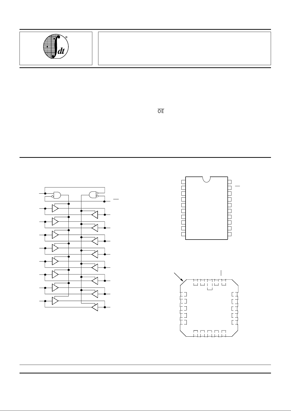
The FCT3245/A octal transceivers are built using advanced dual metal CMOS technology. These high-speed,
low-power transceivers are ideal for synchronous communication between two busses (A and B). The direction control
pin (DIR) controls the direction of data flow. The output enable
pin (OE) overrides the direction control and disables both
ports. All inputs are designed with hysteresis for improved
noise margin.
The FCT3245/A have series current limiting resistors.
These offer low ground bounce, minimal undershoot, and
controlled output fall times-reducing the need for external
series terminating resistors.
DESCRIPTION:
DIR
OE
A
1
A
2
A
3
A
4
A
5
A
6
A
7
A
8
B
1
B
2
B
3
B
4
B
5
B
6
B
7
B
8
2650 drw 01
3.3V CMOS OCTAL
BIDIRECTIONAL
TRANSCEIVERS
IDT54/74FCT3245/A
FEATURES:
• 0.5 MICRON CMOS Technology
• ESD > 2000V per MIL-STD-883, Method 3015;
> 200V using machine model (C = 200pF, R = 0)
• 25 mil Center SSOP and QSOP Packages
• Extended commercial range of -40°C to +85°C
•V
CC = 3.3V ±0.3V, Normal Range or
VCC = 2.7V to 3.6V, Extended Range
• CMOS power levels (0.4µW typ. static)
• Rail-to-Rail output swing for increased noise margin
• Military product compliant to MIL-STD-883, Class B
2650 drw 02
FUNCTIONAL BLOCK DIAGRAM
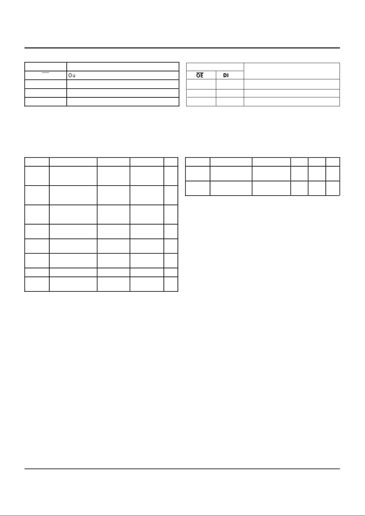
PIN CONFIGURATIONS
2650 drw 03
1
INDEX
A3
DIR
V
CC
LCC
TOP VIEW
3 2 20 19
1
4
5
6
7
8
18
17
16
15
14
9 10111213
L20-2
A4
A5
A6
A7
A2
B7
A8
B6
GND
B
8
OE
B2
B1
B3
B4
B5
A1
The IDT logo is a registered trademark of Integrated Device Technology, Inc.
5
6
7
8
9
10
1
2
3
4
20
19
18
17
16
15
14
13
12
11GND
A
1
A
2
A3
DIR
A
4
A5
A6
A7
A
8
B
B
B
B
B
B
B
B
Vcc
1
OE
2
3
4
5
6
7
8
P20-1
D20-1
SO20-2
SO20-7
SO20-8
&
E20-1
DIP/SOIC/SSOP/QSOP/CERPACK
TOP VIEW
IDT54/74FCT3245/A
3.3V CMOS OCTAL BIDIRECTIONAL TRANSCEIVERS MILITARY AND COMMERCIAL TEMPERATURE RANGES
8.12 2
FUNCTION TABLE
(1)
Inputs
OE
OE
DIR Outputs
L L Bus B Data to Bus A
L H Bus A Data to Bus B
H X High Z State
NOTE:
1. H = HIGH Voltage Level
L = LOW Voltage Level
X = Don't Care
Z = High Impedance
NOTE:
1. This parameter is measured at characterization but not tested.
PIN DESCRIPTION
ABSOLUTE MAXIMUM RATINGS
(1)
2650 tbl 02
CAPACITANCE (TA = +25°C, f = 1.0MHz)
2650 lnk 04
2650 tbl 01
Symbol Rating Commercial Military Unit
VTERM
(2)
Terminal Voltage
with Respect to
GND
–0.5 to +4.6 –0.5 to +4.6 V
VTERM
(3)
Terminal Voltage
with Respect to
GND
–0.5 to +7.0 –0.5 to +7.0 V
VTERM
(4)
Terminal Voltage
with Respect to
GND
–0.5 to
V
CC + 0.5
–0.5 to
VCC + 0.5
V
TA Operating
Temperature
–40 to +85 –55 to +125 °C
TBIAS Temperature
Under Bias
–55 to +125 –65 to +135 °C
TSTG Storage
Temperature
–55 to +125 –65 to +150 °C
PT Power Dissipation 1.0 1.0 W
IOUT DC Output
Current
–60 to +60 –60 to +60 mA
2650 lnk 03
Symbol Parameter
(1)
Conditions Typ. Max. Unit
CIN Input
Capacitance
VIN = 0V 3.5 6.0 pF
CI/O I/O
Capacitance
VOUT = 0V 4.0 8.0 pF
NOTES:
1. Stresses greater than those listed under ABSOLUTE MAXIMUM RATINGS may cause permanent damage to the device. This is a stress rating
only and functional operation of the device at these or any other conditions above those indicated in the operational sections of this specification is not implied. Exposure to absolute maximum rating conditions for
extended periods may affect reliability.
2. Vcc terminals.
3. Input terminals.
4. Output and I/O terminals.
Pin Names Description
OE
Output Enable Input (Active LOW)
DIR Direction Control Input
Ax Side A Inputs or 3-State Outputs
Bx Side B Inputs or 3-State Outputs
 Loading...