

Integrated Device Technology Inc IDT74FCT3244PYB, IDT74FCT3244PY, IDT74FCT3244PB, IDT74FCT3244P, IDT74FCT3244DB Datasheet
...
Integrated Device Technology, Inc.
DESCRIPTION:
The FCT3244/A octal buffer/line drivers are built using
advanced dual metal CMOS technology. These high-speed,
low-power buffers are designed to be used as memory data
and address drivers, clock drivers, and bus-oriented transmitter/receivers. The three-state controls are designed to operate these devices in a dual-nibble or single-byte mode. All
inputs are designed with hysteresis for improved noise margin.
IDT54/74FCT3244/A
3.3V CMOS OCTAL
BUFFER/LINE DRIVER
1Y1
1
Y
2
1
Y
3
1
Y
4
1
A
1
1A2
1
A
3
1
A
4
2
OE
2A1
2A2
2
A
3
2
A
4
2
Y
1
2
Y
2
2
Y
3
2
Y
4
2779 drw 01
1
OE
The IDT logo is a registered trademark of Integrated Device Technology, Inc.
1
2779 drw 02
FEATURES:
• 0.5 MICRON CMOS Technology
• ESD > 2000V per MIL-STD-883, Method 3015;
> 200V using machine model (C = 200pF, R = 0)
• 25 mil Center SSOP and QSOP Packages
• Extended commercial range of -40°C to +85°C
•V
CC = 3.3V ±0.3V, Normal Range or
VCC = 2.7V to 3.6V, Extended Range
• CMOS power levels (0.4µW typ. static)
• Rail-to-Rail output swing for increased noise margin
• Military product compliant to MIL-STD-883, Class B
MILITARY AND COMMERCIAL TEMPERATURE RANGES DECEMBER 1995
1996 Integrated Device Technology, Inc. 8.11 DSC-2779/4
PIN CONFIGURATIONSFUNCTIONAL BLOCK DIAGRAM
5
6
7
8
9
10
1
2
3
4
20
19
18
17
16
15
14
13
12
11GND
A
1
Y
4
A2
1
OE
Y
3
A3
Y2
A4
Y
1
1
Y
2A
1Y
2A
1Y
2A
1Y
2A
Vcc
1
2
OE
4
2
3
3
2
4
1
P20-1
D20-1
SO20-2
SO20-7
&
SO20-8
1
2
1
2
1
2
1
2
DIP/SOIC/SSOP/QSOP
TOP VIEW
IDT54/74FCT3244/A
3.3V CMOS OCTAL BUFFER/LINE DRIVER MILITARY AND COMMERCIAL TEMPERATURE RANGES
8.11 2
NOTE:
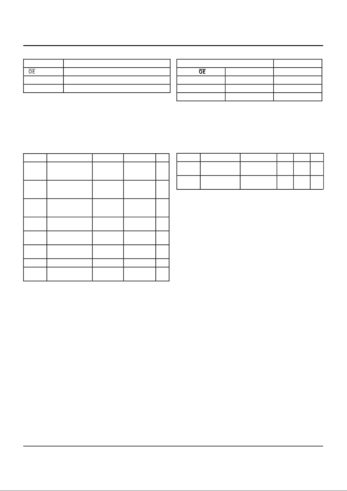
1. H = HIGH Voltage Level
X = Don’t Care
L = LOW Voltage Level
Z = High Impedance
PIN DESCRIPTION
ABSOLUTE MAXIMUM RATINGS
(1)
CAPACITANCE (TA = +25°C, f = 1.0MHz)
FUNCTION TABLE
(1)
2779 tbl 01
2779 tbl 02
2779 lnk 04
NOTE:
1. This parameter is measured at characterization but not tested.
Symbol Rating Commercial Military Unit
VTERM
(2)
Terminal Voltage
with Respect to
GND
–0.5 to +4.6 –0.5 to +4.6 V
VTERM
(3)
Terminal Voltage
with Respect to
GND
–0.5 to +7.0 –0.5 to +7.0 V
VTERM
(4)
Terminal Voltage
with Respect to
GND
–0.5 to
V
CC + 0.5
–0.5 to
VCC + 0.5
V
TA Operating
Temperature
–40 to +85 –55 to +125 °C
TBIAS Temperature
Under Bias
–55 to +125 –65 to +135 °C
TSTG Storage
Temperature
–55 to +125 –65 to +150 °C
PT Power Dissipation 1.0 1.0 W
IOUT DC Output
Current
–60 to +60 –60 to +60 mA
2779 lnk 03
Symbol Parameter
(1)
Conditions Typ. Max. Unit
C
IN
Input
Capacitance
VIN = 0V 3.5 6.0
pF
C
OUT
Output
Capacitance
V
OUT
= 0V 4.0 8.0
pF
NOTES:
1. Stresses greater than those listed under ABSOLUTE MAXIMUM RATINGS may cause permanent damage to the device. This is a stress rating
only and functional operation of the device at these or any other conditions
above those indicated in the operational sections of this specification is
not implied. Exposure to absolute maximum rating conditions for extended periods may affect reliability.
2. Vcc terminals.
3. Input terminals.
4. Output and I/O terminals.
Pin Names Description
x
OE
3–State Output Enable Inputs (Active LOW)
xAx Data Inputs
xYx 3-State Outputs
Inputs Outputs
x
OEOE xAx xYx
LL
L
LHH
HXZ
 Loading...