

Integrated Device Technology Inc IDT74FCT273P, IDT74FCT273LB, IDT74FCT273L, IDT74FCT273EB, IDT74FCT273E Datasheet
...
Integrated Device Technology, Inc.
FAST CMOS
OCTAL FLIP-FLOP
WITH MASTER RESET
IDT54/74FCT273
IDT54/74FCT273A
IDT54/74FCT273C
FEATURES:
• IDT54/74FCT273 equivalent to FAST speed;
• IDT54/74FCT273A 45% faster than FAST
• IDT54/74FCT273C 55% faster than FAST
• Equivalent to FAST output drive over full temperature
and voltage supply extremes
•IOL = 48mA (commercial) and 32mA (military)
• CMOS power levels (1mW typ. static)
• TTL input and output level compatible
• CMOS output level compatible
• Substantially lower input current levels than FAST
(5µA max.)
• Octal D flip-flop with Master Reset
• JEDEC standard pinout for DIP and LCC
• Product available in Radiation Tolerant and Radiation
Enhanced versions
• Military product compliant to MIL-STD-883, Class B
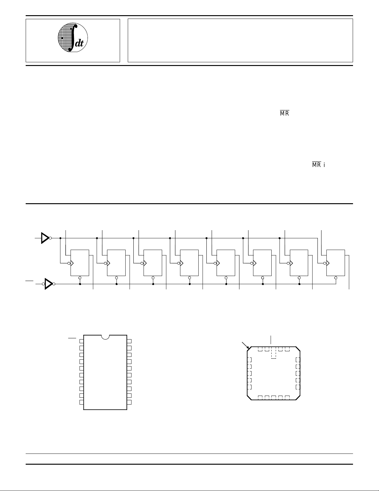
FUNCTIONAL BLOCK DIAGRAM
2
D
D
Q
CP
R
D
CP
0
D
D
Q
CP
R
D
1
D
D
Q
CP
R
D
DESCRIPTION:
The IDT54/74FCT273/A/C are octal D flip-flops built using
an advanced dual metal CMOS technology. The IDT54/
74FCT273/A/C have eight edge-triggered D-type flip-flops
with individual D inputs and O outputs. The common buffered
Clock (CP) and Master Reset (MR) inputs load and reset
(clear) all flip-flops simultaneously.
The register is fully edge-triggered. The state of each D
input, one set-up time before the LOW-to-HIGH clock
transition, is transferred to the corresponding flip-flop’s O
output.
All outputs will be forced LOW independently of Clock or
Data inputs by a LOW voltage level on the MR input. The
device is useful for applications where the true output only is
required and the Clock and Master Reset are common to all
storage elements.
3
D
D
Q
CP
R
D
4
D
D
Q
CP
R
D
5
D
D
Q
CP
R
D
6
D
D
Q
CP
R
D
7
D
D
Q
CP
R
D
MR
O
0
O
1
O
2
O
3
O
4
O
5
O
6
O
2558 drw 01
PIN CONFIGURATIONS
0
MR
O0
D0
D1
O1
O2
D2
D3
O3
GND
1
2
3
4
5
6
7
8
9
10
P20-1
D20-1
SO20-2
&
E20-1
20
Vcc
19
O7
18
17
16
15
14
13
12
11
D
D
O6
O5
D5
D4
O
CP
7
6
4
INDEX
D1
O1
O2
D2
D3
D
32
4
5
6
7
8
10 11 12 13
9
0
O
L20-2
O3
GND
DIP/SOIC/CERPACK
TOP VIEW
The IDT logo is a registered trademark of Integrated Device Technology, Inc.
FAST is a registered trademark of National Semiconductor Co.
LCC
TOP VIEW
MILITARY AND COMMERCIAL TEMPERATURE RANGES MAY 1992
1992 Integrated Device Technology, Inc. 7.10 DSC-4609/2
1
MR
20 19
CP
Vcc
4
O
7
O
18
17
16
15
14
4
D
D7
D6
O6
O5
D5
2558 drw 02
1
7
IDT54/74FCT273/A/C FAST CMOS
OCTAL D FLIP-FLOP WITH MASTER RESET MILITARY AND COMMERCIAL TEMPERATURE RANGES
PIN DESCRIPTION
Pin Names Description
N Data Input
D
MR
CP Clock Pulse Input (Active Rising Edge)
N Data Outputs
O
ABSOLUTE MAXIMUM RATINGS
Symbol Rating Commercial Military Unit
(2)
TERM
V
V
TERM
T
A Operating 0 to +70 –55 to +125 °C
T
BIAS Temperature –55 to +125 –65 to +135 °C
STG Storage –55 to +125 –65 to +150 ° C
T
P
T Power Dissipation 0.5 0.5 W
OUT DC Output Current 120 120 mA
I
NOTES: 2558 tbl 01
1. Stresses greater than those listed under ABSOLUTE MAXIMUM
RATINGS may cause permanent damage to the device. This is a stress
rating only and functional operation of the device at these or any other
conditions above those indicated in the operational sections of this
specification is not implied. Exposure to absolute maximum rating
conditions for extended periods may affect reliability. No terminal voltage
may exceed V
2. Input and V
3. Outputs and I/O terminals only.
Terminal Voltage –0.5 to +7.0 –0.5 to +7.0 V
with Respect
to GND
(3)
Terminal Voltage –0.5 to VCC –0.5 to VCC V
with Respect
to GND
Temperature
Under Bias
Temperature
CC terminals only.
Master Reset (Active LOW)
2558 tbl 05
(1)
CC by +0.5V unless otherwise noted.
FUNCTION TABLE
Inputs Outputs
Operating Mode
MR
MR
CP D
N ON
Reset (Clear) L X X L
Load “1” H ↑ hH
Load “0” H ↑ lL
NOTES: 2558 tbl 06
H = HIGH voltage level steady-state
h = HIGH voltage level one set-up time prior to the LOW-to-HIGH clock
transition
L = LOW voltage level steady state
l = LOW voltage level one set-up time prior to the LOW-to-HIGH clock
transition
X = Don’t care
↑ = LOW-to-HIGH clock transition
CAPACITANCE (TA = +25°C, f = 1.0MHz)
Symbol Parameter
IN Input Capacitance VIN = 0V 6 10 pF
C
OUT Output Capacitance V OUT = 0V 8 12 pF
C
NOTE: 2558 tbl 02
1. This parameter is guaranteed by characterization data and not tested.
(1)
Conditions Typ. Max. Unit
7.10 2
IDT54/74FCT273/A/C FAST CMOS
OCTAL D FLIP-FLOP WITH MASTER RESET MILITARY AND COMMERCIAL TEMPERATURE RANGES
DC ELECTRICAL CHARACTERISTICS OVER OPERATING RANGE
Following Conditions Apply Unless Otherwise Specified: VLC = 0.2V; VHC = VCC – 0.2V
Commercial: TA = 0°C to +70°C, VCC = 5.0V ± 5%; Military: TA = –55°C to +125°C, VCC = 5.0V ± 10%
Symbol Parameter Test Conditions
IH Input HIGH Level Guaranteed Logic HIGH Level 2.0 — — V
V
IL Input LOW Level Guaranteed Logic LOW Level — — 0.8 V
V
IH Input HIGH Current VCC = Max. VI = VCC ——5µA
I
(1)
I = 2.7V — — 5
V
Min. Typ.
IIL Input LOW Current VI = 0.5V — — –5
VI = GND — — –5
IK Clamp Diode Voltage Vcc = Min., IN = –18mA — –0.7 –1.2 V
V
OS Short Circuit Current Vcc = Max.
I
OH Output HIGH Voltage Vcc = 3V, VIN = VLC or VHC, IOH = –32µAVHC VCC —V
V
Vcc = Min. I
IN = VIH or VIL IOH = –12mA MIL. 2.4 4.3 —
V
OL Output LOW Voltage Vcc = 3V, VIN = VLC or VHC, IOL = 300µA — GND VLC V
V
Vcc = Min. I
(3)
, VO = GND –60 –120 — mA
OH = –300µAVHC VCC —
OH = –15mA COM’L. 2.4 4.3 —
I
OL = 300µA — GND VLC
VIN = VIH or VIL IOL = 32mA MIL. — 0.3 0.5
OL = 48mA COM’L. — 0.3 0.5
I
NOTES: 2558 tbl 03
1. For conditions shown as Max. or Min., use appropriate value specified under Electrical Characteristics for the applicable device type.
2. Typical values are at V
3. Not more than one output should be shorted at one time. Duration of the short circuit test should not exceed one second.
4. This parameter is guaranteed but not tested.
CC = 5.0V, +25°C ambient and maximum loading.
(2)
Max. Unit
(4)
(4)
(4)
7.10 3
 Loading...