

IDT IDT54FCT157T, IDT54FCT157AT, IDT54FCT157CT, IDT54FCT157DT, IDT54FCT257T User Manual
...
查询IDT54FCT157ATD供应商
FAST CMOS
QUAD 2-INPUT
MULTIPLEXER
Integrated Device Technology, Inc.
FEATURES:
• Common features:
– Low input and output leakage ≤1µA (max.)
– CMOS power levels
– True TTL input and output compatibility
– VOH = 3.3V (typ.)
– VOL = 0.3V (typ.)
– Meets or exceeds JEDEC standard 18 specifications
– Product available in Radiation Tolerant and Radiation
Enhanced versions
– Military product compliant to MIL-STD-883, Class B
and DESC listed (dual marked)
– Available in DIP, SOIC, SSOP, QSOP, CERPACK
and LCC packages
• Features for FCT157T/257T:
– Std., A, C and D speed grades
– High drive outputs (-15mA IOH, 48mA IOL)
• Features for FCT2257T:
– Std., A, and C speed grades
– Resistor outputs (-15mA I
(-12mA IOH, 12mA IOL Mil.)
– Reduced system switching noise
OH, 12mA IOL Com.)
IDT54/74FCT157T/AT/CT/DT
IDT54/74FCT257T/AT/CT/DT
IDT54/74FCT2257T/AT/CT
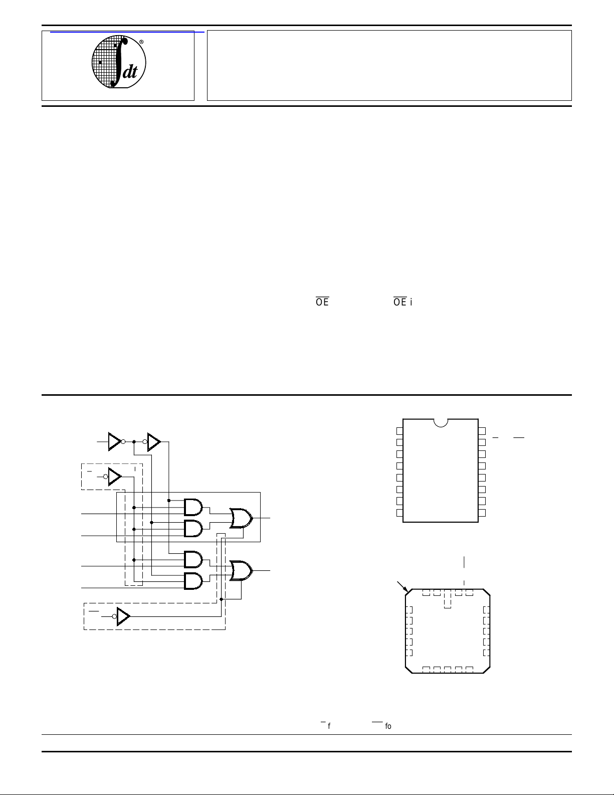
DESCRIPTION:
The FCT157T, FCT257T/FCT2257T are high-speed quad
2-input multiplexers built using an advanced dual metal CMOS
technology. Four bits of data from two sources can be
selected using the common select input. The four buffered
outputs present the selected data in the true (non-inverting)
form.
The FCT157T has a common, active-LOW, enable input.
When the enable input is not active, all four outputs are held
LOW. A common application of ‘FCT157T is to move data
from two different groups of registers to a common bus.
Another application is as a function generator. The ‘FCT157T
can generate any four of the 16 different functions of two
variables with one variable common.
The FCT257T/FCT2257T have a common Output Enable
(OE) input. When OE is HIGH, all outputs are switched to a
high-impedance state allowing the outputs to interface directly
with bus-oriented systems.
The FCT2257T has balanced output drive with current
limiting resistors. This offers low ground bounce, minimal
undershoot and controlled output fall times-reducing the need
for external series terminating resistors. FCT2xxxT parts are
plug-in replacements for FCTxxxT parts.
FUNCTIONAL BLOCK DIAGRAM
S
157 Only
1B–I1D
I
I0B–I
E
3 other multiplexers
0D
1A
I
0A
I
OE257 Only
Z B–Z D
A
Z
2537 drw 01
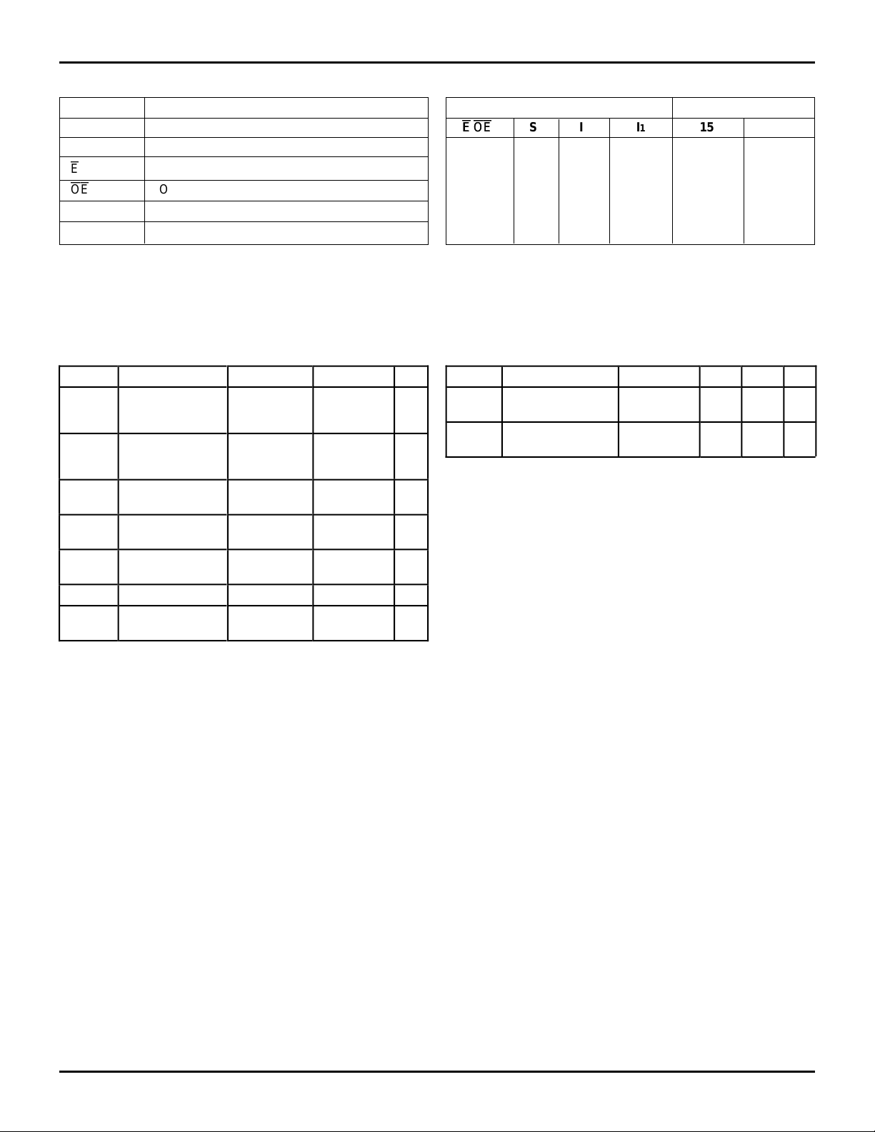
PIN CONFIGURATIONS
1
S
I
I
GND
2
0A
1A
Z
A
I
0B
I
1B
B
Z
3
4
5
6
7
8
P16-1,
D16-1,
SO16-1,
SO16-7
E16-1
DIP/SOIC/QSOP/CERPACK
TOP VIEW
INDEX
1A
I
ZA
NC NC
I0B
I1B
0A
I
32
4
5
6
7
8
10 11 12 13
9
ZB
LCC
&
NC
S
1
L20-2
NC
GND
Vcc
20 19
ZDI
16
15
14
13
12
11
10
9
E or OE*
18
17
16
15
14
1D
Vcc
E or OE*
I
0C
I
1C
Z
C
I
0D
I
1D
D
Z
I0C
I
1C
ZC
I
0D
2537 drw 02
2537 drw 03
TOP VIEW
The IDT logo is a registered trademark of Integrated Device Technology, Inc.
* E for FCT157, OE for FCT257/FCT2257.
MILITARY AND COMMERCIAL TEMPERATURE RANGES JUNE 1996
1996 Integrated Device Technology, Inc. 6.6 2537/6
1
IDT54/74FCT157T/AT/CT/DT, IDT54/74FCT257T/AT/CT/DT- 2257T/AT/CT
FAST CMOS QUAD 2-INPUT MULTIPLEXER MILITARY AND COMMERCIAL TEMPERATURE RANGES
PIN DESCRIPTION
Pin Names Description
0A–I0D Source 0 Data Inputs
I
1A–I1D Source 1 Data Inputs
I
E
OE
S Select Input
A–ZD Outputs
Z
ABSOLUTE MAXIMUM RATINGS
Symbol Rating Commercial Military Unit
(2)
VTERM
(3)
VTERM
TA Operating
TBIAS Temperature
TSTG Storage
PT Power Dissipation 0.5 0.5 W
IOUT DC Output
NOTES:
1. Stresses greater than those listed under ABSOLUTE MAXIMUM RATINGS may cause permanent damage to the device. This is a stress rating
only and functional operation of the device at these or any other conditions
above those indicated in the operational sections of this specification is
not implied. Exposure to absolute maximum rating conditions for
extended periods may affect reliability. No terminal voltage may exceed
V
CC by +0.5V unless otherwise noted.
2. Input and V
3. Outputs and I/O terminals only.
Enable Input (Active LOW)–FCT157T
Output Enable (Active LOW)–FCT257T/2257T
(1)
Terminal Voltage
–0.5 to +7.0 –0.5 to +7.0 V
with Respect to
GND
Terminal Voltage
with Respect to
GND
–0.5 to
CC +0.5
V
–0.5 to
VCC +0.5
0 to +70 –55 to +125 °C
Temperature
–55 to +125 –65 to +135 °C
Under Bias
–55 to +125 –65 to +150 °C
Temperature
–60 to +120 –60 to +120 mA
Current
CC terminals only.
2537 tbl 01
V
2537 lnk 03
FUNCTION TABLE
(1)
Inputs Output ZN
EE/
OE
OE
SI0 I1 157 257
HXXX L Z
LHXL L L
LHXH H H
LLLX L L
LLHX H H
NOTE: 2537 tbl 02
1. H = HIGH Voltage Level
L = LOW Voltage Level
X = Don’t Care
Z = High Impedance
CAPACITANCE (TA = +25°C, f = 1.0MHz)
Symbol Parameter
C
IN
Input
Capacitance
C
OUT
Output
Capacitance
NOTE:
1. This parameter is measured at characterization but not tested.
(1)
Conditions Typ. Max. Unit
VIN = 0V 6 10
V
OUT
= 0V 8 12
pF
pF
2537 lnk 04
6.6 2
IDT54/74FCT157T/AT/CT/DT, IDT54/74FCT257T/AT/CT/DT - 2257T/AT/CT
FAST CMOS QUAD 2-INPUT MULTIPLEXER MILITARY AND COMMERCIAL TEMPERATURE RANGES
DC ELECTRICAL CHARACTERISTICS OVER OPERATING RANGE
Following Conditions Apply Unless Otherwise Specified:
Commercial: TA = 0°C to +70°C, VCC = 5.0V ± 5%; Military: TA = –55°C to +125°C, VCC = 5.0V ± 10%
Symbol Parameter Test Conditions
V
IH
V
IL
I
I H
I
I L
I
OZH
I
OZL
II Input HIGH Current
V
IK
V
H
I
CC
Input HIGH Level Guaranteed Logic HIGH Level 2.0 — — V
Input LOW Level Guaranteed Logic LOW Level — — 0.8 V
Input HIGH Current
Input LOW Current
(4)
(4)
VI = 0.5V — —
VCC = Max. VI = 2.7V — —
High Impedance Output Current VCC = Max. VO = 2.7V — —
(4)
(4)
VCC = Max., VI = V
—
CC
(Max.) — —
IN
= –18mA — –0.7 –1.2 V
(3-State Output pins)
Clamp Diode Voltage VCC = Min., I
Input Hysteresis
Quiescent Power Supply Current VCC = Max., VIN = GND or V
OUTPUT DRIVE CHARACTERISITICS FOR FCT157/257T
Symbol Parameter Test Conditions
V
V
I
OS
I
OFF
OH
OL
Output HIGH Voltage VCC = Min.
IN
= V
IH
or V
V
IL
Output LOW Voltage VCC = Min.
IN
= V
IH
or V
V
IL
Short Circuit Current VCC = Max., VO = GND
Input/Output Power Off Leakage
(5)
VCC = 0V, VIN or VO ≤ 4.5V — —
(3)
(1)
Min. Typ.
VO = 0.5V — —
— 200 — mV
CC
(1)
IOH = –6mA MIL.
OH
= –8mA COM'L.
I
IOH = –12mA MIL.
OH
= –15mA COM'L.
I
I
OL
= 32mA MIL.
OL
= 48mA COM'L.
I
— 0.01 1 mA
Min. Typ.
2.4 3.3 — V
2.0 3.0 — V
— 0.3 0.50 V
–60 –120 –225 mA
(2)
Max. Unit
±
±
±
±
±
(2)
Max. Unit
±
1
1
1
1
1
1
µ
A
µ
A
µ
A
2537 lnk 05
µ
A
2537 tbl 06
OUTPUT DRIVE CHARACTERISTICS FOR FCT2257T
Symbol Parameter Test Conditions
I
ODL
I
ODH
V
OH
V
OL
NOTES:
1. For conditions shown as Max. or Min., use appropriate value specified under Electrical Characteristics for the applicable device type.
2. Typical values are at Vcc = 5.0V, +25°C ambient.
3. Not more than one output should be shorted at one time. Duration of the short circuit test should not exceed one second.
4. The test limit for this parameter is ±5µA at T
5. This parameter is guaranteed but not tested.
Output LOW Current VCC = 5V, V
Output HIGH Current VCC = 5V, V
Output HIGH Voltage VCC = Min.
IN
= V
IH
V
or V
Output LOW Voltage VCC = Min.
IN
= V
IH
V
A = –55°C.
or V
IN
= V
IH or VIL, VOUT
IN
= V
IH
IL
IL
or V
IL,VOUT
(1)
(3)
= 1.5V
(3)
= 1.5V
IOH = –12mA MIL.
OH
= –15mA COM'L.
I
Min. Typ.
16 48 — mA
–16 –48 — mA
2.4 3.3 — V
IOL = 12mA — 0.3 0.50 V
(2)
Max. Unit
2537 lnk 07
6.6 3
 Loading...