

Integrated Device Technology Inc IDT74FCT16H952CTPAB, IDT74FCT16H952CTPA, IDT74FCT16H952CTEB, IDT74FCT16H952CTE, IDT74FCT16H952BTPVB Datasheet
...
Integrated Device Technology, Inc.
FEATURES:
• High-speed 16-bit bus exchange for interbus communication in the following environments:
— Multi-way interleaving memory
— Multiplexed address and data busses
• Direct interface to R3051 family RISChipSet
— R3051 family of integrated RISController CPUs
— R3721 DRAM controller
• Data path for read and write operations
• Low noise 12mA TTL level outputs
• Bidirectional 3-bus architecture: X, Y, Z
— One CPU bus: X
— Two (interleaved or banked) memory busses:Y & Z
— Each bus can be independently latched
• Byte control on all three busses
• Source terminated outputs for low noise and undershoot
control
• 68-pin PLCC and 80-pin PQFP package
• High-performance CMOS technology.
16-BIT TRI-PORT
BUS EXCHANGER
COMMERCIAL TEMPERATURE RANGE AUGUST 1995
1995 Integrated Device Technology, Inc. 11.5 DSC-2046/6
IDT73720/A
DESCRIPTION:
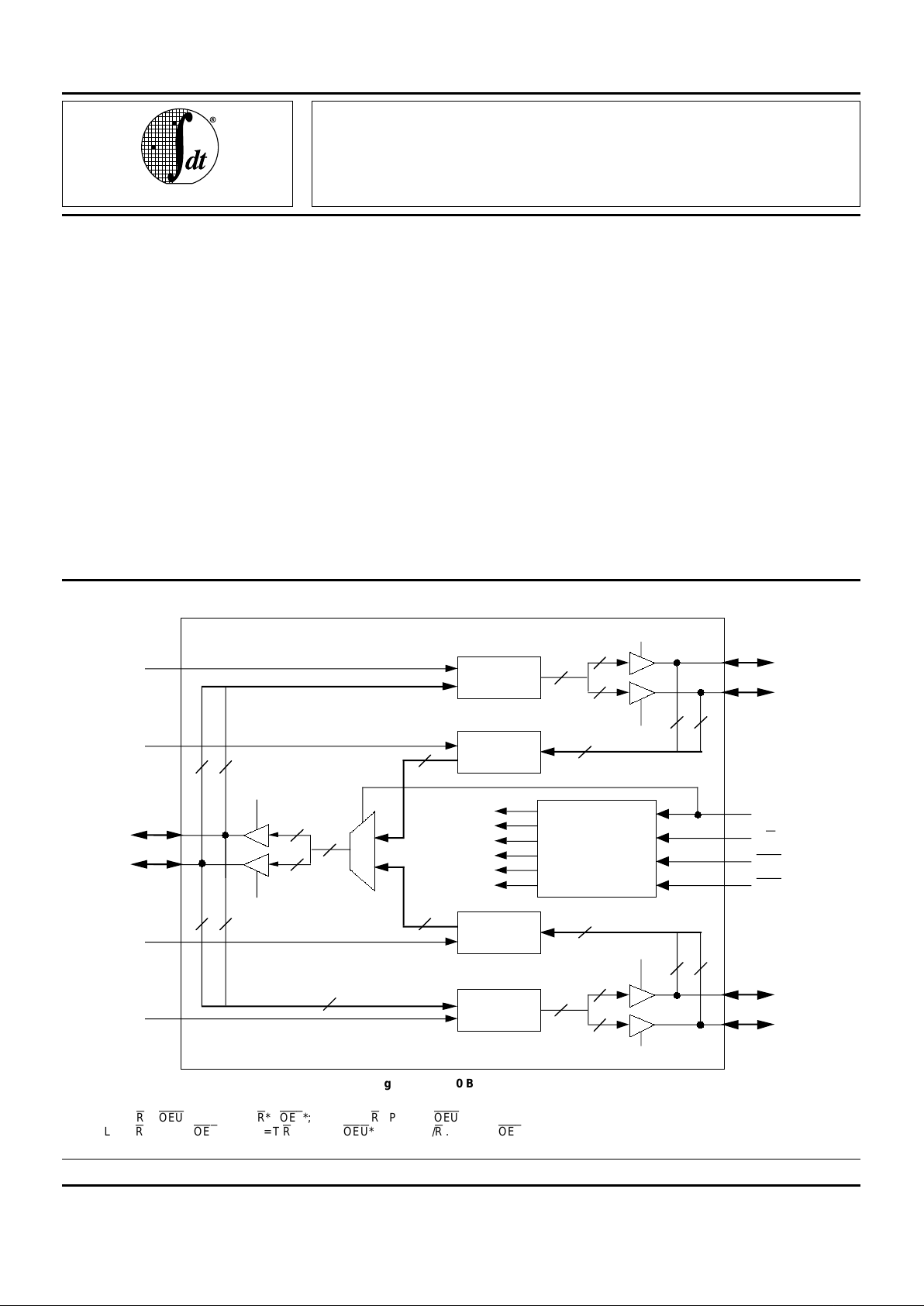
The IDT73720/A Bus Exchanger is a high speed 16-bit bus
exchange device intended for inter-bus communication in
interleaved memory systems and high performance multiplexed address and data busses.
The Bus Exchanger is responsible for interfacing between
the CPU A/D bus (CPU address/data bus) and multiple
memory data busses.
The 73720/A uses a three bus architecture (X, Y, Z), with
control signals suitable for simple transfer between the CPU
bus (X) and either memory bus (Y or Z). The Bus Exchanger
features independent read and write latches for each memory
bus, thus supporting a variety of memory strategies. All three
ports support byte enable to independently enable upper and
lower bytes.
RISChipSet, RISController, R305x, R3051, R3052 are trademarks and the IDT logo is a registered trademark of Integrated Device Technology, Inc.
FUNCTIONAL BLOCK DIAGRAM
NOTE:
1. Logic equations for bus control:
OEXU = T/R* .
OEU
*; OEXL = T/R* .
OEL
*; OEYU = T/R . PATH .
OEU
*
OEYL = T/R . PATH .
OEL
*; OEZU = T/R . PATH* .
OEU
*; OEZL = T/R . PATH* .
OEL
*
Figure 1. 73720 Block Diagram
1
Y-WRITE
LATCH
BUS CONTROL
PATH
LEXY
LEYX
(Even Path)
LEZX
16
8
8
OEYL
OEYU
88
M
U
X
16
OEXL
OEXU
16
OEXU
Y0:7
Y8:15
X0:7
X8:15
Y-READ
LATCH
16
88
16
OEXL
OEYU
OEYL
OEZU
OEZL
Z-READ
LATCH
88
16
T/R
OEU
OEL
Z-WRITE
LATCH
LEXZ
(Odd Path)
16
8
8
OEZL
OEZU
88
Z0:7
Z8:15
16
2527 drw 01
8
8
IDT73720/A 16-BIT TRI-PORT BUS EXCHANGER COMMERCIAL TEMPERATURE RANGE
11.5 2
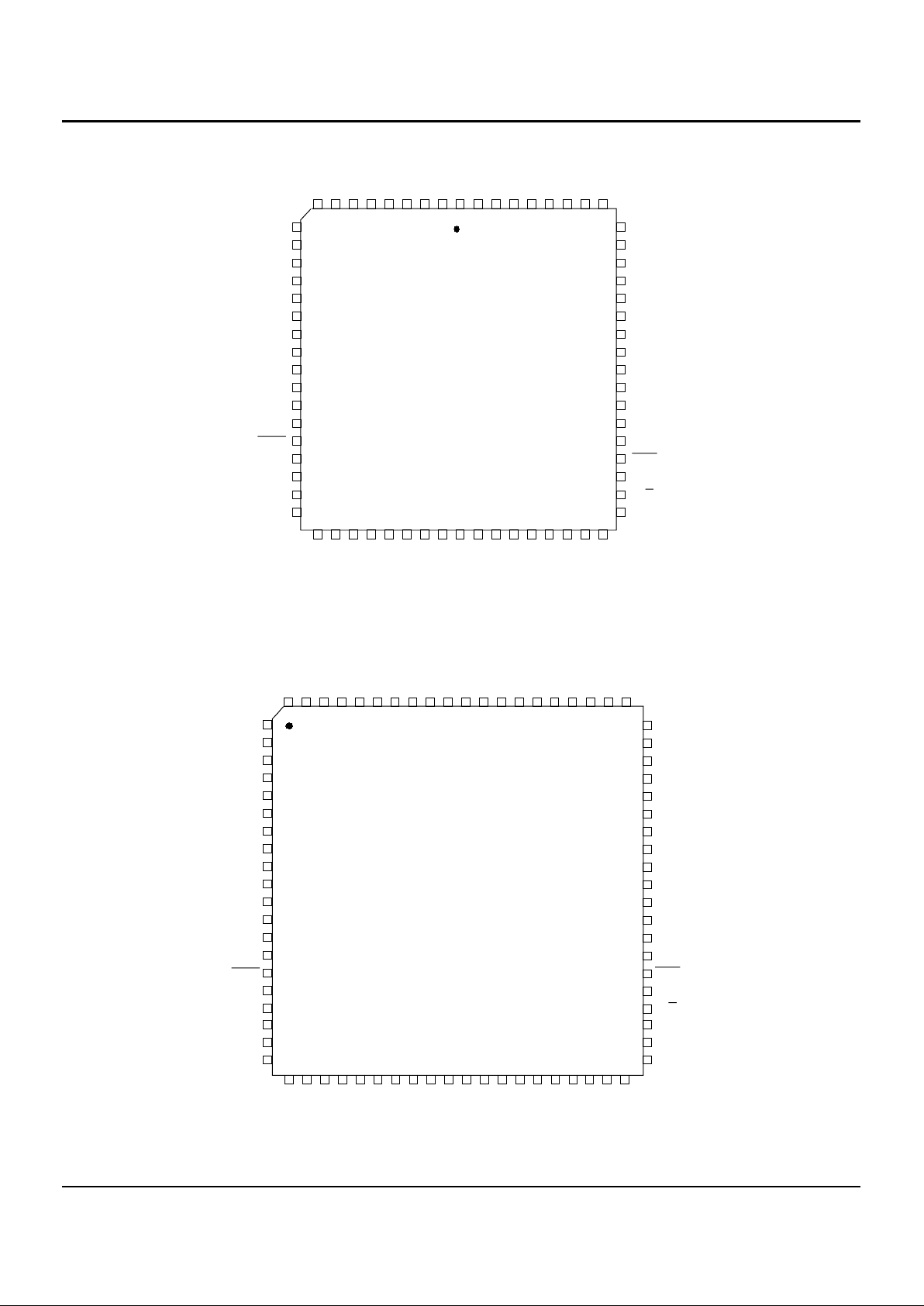
PIN CONFIGURATIONS
PLCC
TOP VIEW
PQFP
TOP VIEW
10
11
12
13
14
15
16
17
18
19
20
21 22 23 24 25 26 27 28 29 30 31 32 33 34 35 36 37 38 39 40
41
42
43
60
59
58
57
56
55
54
53
52
51
50
49
48
47
46
45
44
8
7
6
5
4
3
2
1
68 67 66 65 64 63 62 61
PQ80-1
Pin 1
Designator
GND
VCC
X7
X6X5X4
X3X2X1
X0
Z15
Z14
Z13
Z12
Z11
Z10
GND
GND
OEL
Z9
Z8
Z7
Z6
Z5
Z4
Z3
Z2
Z1
Z0
GND
VCC
LEXZ
LEXY
T/R
2527 drw 03
GND
X8
X9
X13
X15
GND
X10
X11
X12
X14
VCC
PATH
LEYX
LEZX
Y0
Y1
OEU
NC
NC
GND
9
GND
Y2
Y3
Y4Y5Y6Y7Y8
VCC
Y9
Y10
Y11
Y12
Y13
Y14
Y15
NC
NC
GND
76 75 74 73 72 71 70 6980 79 78 77
GND
NC
NC
GND
NC
NC
GND
10
11
12
13
14
15
16
17
18
19
20
21
22
23
24
25
26
27 28 29 30 31 32 33 34 35 36 37 38 39 40 41 42 43
60
59
58
57
56
55
54
53
52
51
50
49
48
47
46
45
44
9 8 7 6 5 4 3 2 1 686766 6564636261
J68-1
Pin 1
Designator
GND
VCC
X7
X6X5X4X3X2X1X0
Z15
Z14
Z13
Z12
Z11
Z10
GND
GND
Y2
Y3
Y4
Y5
Y6
Y7
Y8
GND
VCC
Y9
Y10
Y11
Y12
Y13
Y14
Y15
OEL
Z9
Z8
Z7
Z6
Z5
Z4
Z3
Z2
Z1
Z0
GND
VCC
LEXZ
LEXY
GND
T/R
GND
X8
X9
X13
X15
GND
X10
X11
X12
X14
VCC
PATH
LEYX
LEZX
Y0
Y1
OEU
2527 drw 02
IDT73720 /A16-BIT TRI-PORT BUS EXCHANGER COMMERCIAL TEMPERATURE RANGE
11.5 3
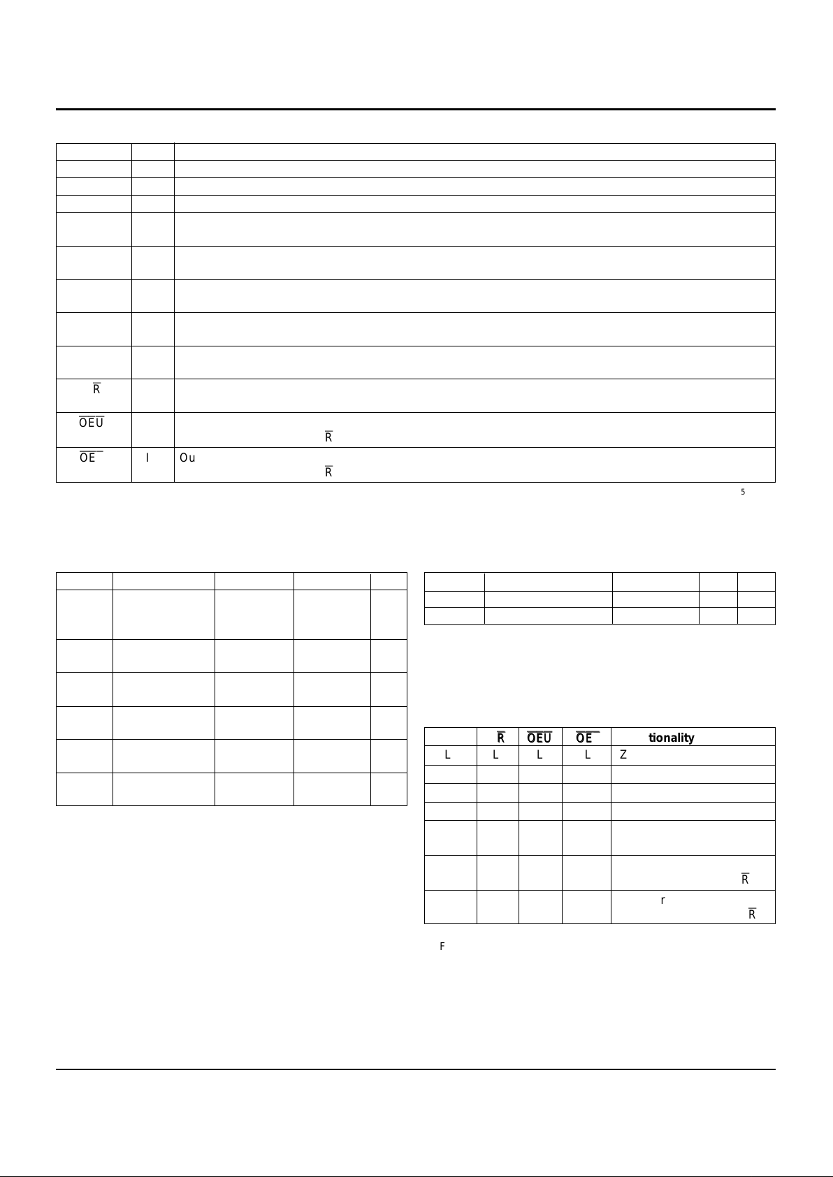
PIN DESCRIPTION
Signal I/O Description
X(0:15) I/O Bidirectional Data Port X. Usually connected to the CPU's A/D (Address/Data) bus.
Y(0:15) I/O Bidirectional Data port Y. Connected to the even path or even bank of memory.
Z(0:15) I/O Bidirectional Data port Z. Connected to the odd path or odd bank of memory.
LEXY I Latch Enable input for Y-Write Latch. The Y-Write Latch is open when LEXY is HIGH. Data from the X-port
(CPU) is latched on the HIGH-to-LOW transition of LEXY
LEXZ I Latch Enable input for Z-Write Latch. The Z-Write Latch is open when LEXZ is HIGH. Data from the X-port
(CPU) is latched on the HIGH-to-LOW transition of LEXZ.
LEYX I Latch Enable input for the Y-Read Latch. The Y-Read Latch is open when LEYX is HIGH. Data from the even
path Y is latched on the HIGH-to-LOW transition of LEYX.
LEZX I Latch Enable input for the Z-Read Latch. The Z-Read Latch is open when LEZX is HIGH. Data from the odd
path Z is latched on the HIGH-to-LOW transition of LEZX
PATH I Even/Odd Path Selection. When high, PATH enables data transfer between the X-Port and the Y-port (even
path). When LOW, PATH enables data transfer between the X-Port and the Z-Port (odd path).
T/
R
I Transmit/Receive Data. When high, Port X is an input Port and either Port Y or Z is an output Port. When LOW,
Port X is an output Port while Ports Y & Z are input Ports
OEU
I Output Enable for Upper byte. When LOW, the Upper byte of data is transfered to the port specified by PATH in
the direction specified by T/R .
OEL
I Output Enable for Lower byte. When LOW, the Lower byte of data is transfered to the port specified by PATH in
the direction specified by T/R .
2527 tbl 02
CAPACITANCE (TA = +25°C, F = 1.0MHZ)
Symbol Parameter
(1)
Conditions Max. Unit
C
IN Input Capacitance VIN = 0V 8 pF
C
OUT Output Capacitance VOUT = 0V 12 pF
NOTE: 2527 tbl 04
1. This parameter is guaranteed by device characterization, but is not production tested.
ABSOLUTE MAXIMUM RATINGS
(1)
Symbol Rating Com’l. Mil. Unit
V
TERM Terminal Voltage –0.5 to +7.0 –0.5 to +7.0 V
with Respect
to GND
TA Operating 0 to +70 –55 to +125 °C
Temperature
T
BIAS Temperature –55 to +125 –65 to +135 °C
Under Bias
T
STG Storage –55 to +125 –65 to +125 °C
Temperature
P
T Power 1.0 1.0 W
Dissipation
I
OUT DC Output 50 50 mA
Current
NOTE: 2527 tbl 03
1. Stresses greater than those listed under ABSOLUTE MAXIMUM
RATINGS may cause permanent damage to the device. This is a stress
rating only and functional operation of the device at these or any other
conditions above those indicated in the operational sections of this
specification is not implied. Exposure to absolute maximum rating
conditions for extended periods may affect reliability.
TRUTH TABLE
Path T/
RROEU
OEU
OEL
OEL
Functionality
LLLLZ→X (16-bits)–Read Z
(1)
LHLLX→Z (16 bits)–Write Z
(1)
HLLLY→X (16-bits)–Read Y
(2)
H H L L X→Y (16 bits)–Write Y
(2)
X X H H All output buffers are
disabled
X X H L Transfer of lower 8 bits
(0:7) as per PATH & T/
R
X X L H Transfer of upper 8 bits
(8:15) as per PATH & T/
R
NOTES: 2527 tbl 01
1. For Z→X and X→Z transfers, Y-port output buffers are tristated.
2. For Y→X and X→Y transfers, Z-port output buffers are tristated.
 Loading...