

IDT IDT54FCT16823AT, IDT54FCT16823BT, IDT54FCT16823CT, IDT54FCT16823ET, IDT54FCT162823AT User Manual
...
Integrated Device Technology, Inc.
FAST CMOS 18-BIT
REGISTER
IDT54/74FCT16823AT/BT/CT/ET
IDT54/74FCT162823AT/BT/CT/ET
FEATURES:
• Common features:
– 0.5 MICRON CMOS Technology
– High-speed, low-power CMOS replacement for
ABT functions
– Typical tSK(o) (Output Skew) < 250ps
– Low input and output leakage ≤1µA (max.)
– ESD > 2000V per MIL-STD-883, Method 3015;
> 200V using machine model (C = 200pF, R = 0)
– Packages include 25 mil pitch SSOP, 19.6 mil pitch
TSSOP, 15.7 mil pitch TVSOP and 25 mil pitch Cerpack
– Extended commercial range of -40°C to +85°C
–V
CC = 5V ±10%
• Features for FCT16823AT/BT/CT/ET:
– High drive outputs (-32mA IOH, 64mA IOL)
– Power off disable outputs permit “live insertion”
– Typical VOLP (Output Ground Bounce) < 1.0V at
VCC = 5V, TA = 25°C
• Features for FCT162823AT/BT/CT/ET:
– Balanced Output Drivers: ±24mA (commercial),
±16mA (military)
– Reduced system switching noise
– Typical VOLP (Output Ground Bounce) < 0.6V at
VCC = 5V,TA = 25°C
DESCRIPTION:
The FCT16823AT/BT/CT/ET and FCT162823AT/BT/CT/
ET 18-bit bus interface registers are built using advanced,
dual metal CMOS technology. These high-speed, low-power
registers with clock enable (x
trols are ideal for parity bus interfacing in high-performance
synchronous systems. The control inputs are organized to
operate the device as two 9-bit registers or one 18-bit register.
Flow-through organization of signal pins simplifies layout. All
inputs are designed with hysteresis for improved noise margin.
The FCT16823AT/BT/CT/ET are ideally suited for driving
high-capacitance loads and low-impedance backplanes. The
output buffers are designed with power off disable capability
to allow "live insertion" of boards when used as backplane
drivers.
The FCT162823AT/BT/CT/ET have balanced output drive
with current limiting resistors. This offers low ground bounce,
minimal undershoot, and controlled output fall times – reducing the need for external series terminating resistors. The
FCT162823AT/BT/CT/ET are plug-in replacements for the
FCT16823AT/BT/CT/ET and ABT16823 for on-board interface applications.
CLKEN
) and clear (x
CLR
) con-
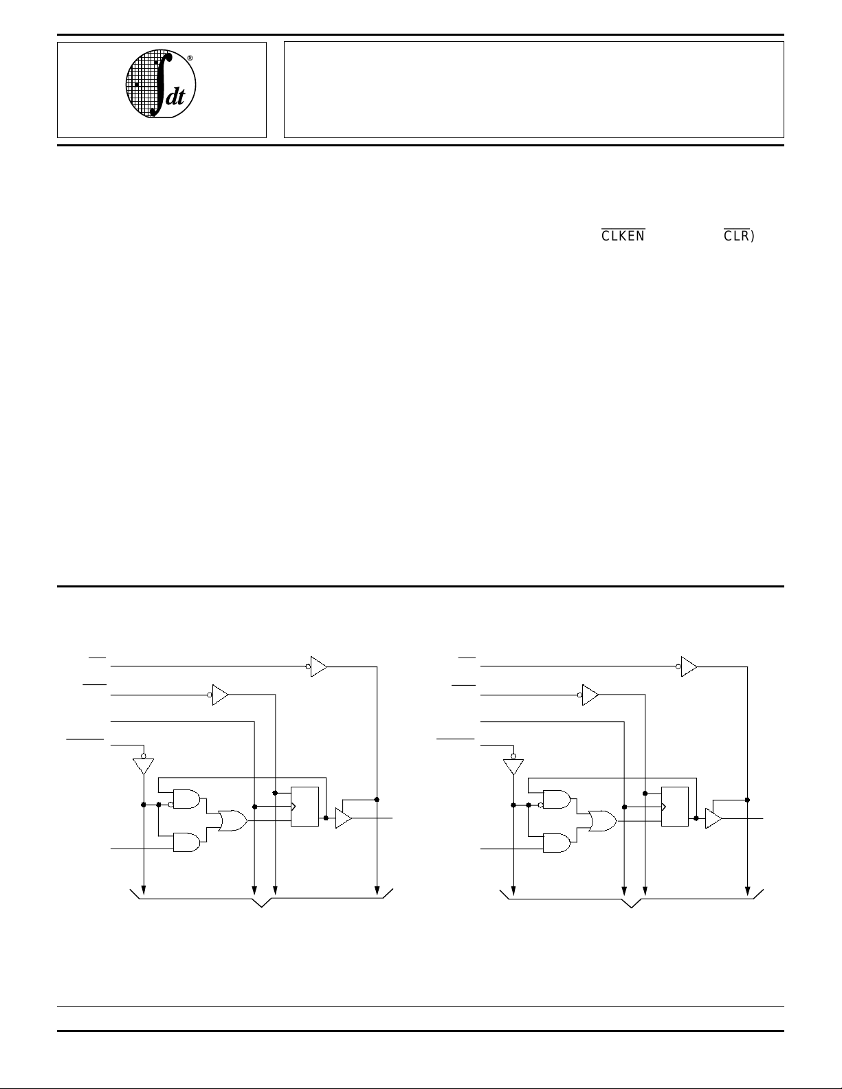
FUNCTIONAL BLOCK DIAGRAM
1OE
1CLR
1CLK
1CLKEN
R
C
D
1D1
TO 8 OTHER CHANNELS
The IDT logo is a registered trademark of Integrated Device Technology, Inc.
Q1
1
2772 drw 01 2772 drw 02
MILITARY AND COMMERCIAL TEMPERATURE RANGES AUGUST 1996
1996 Integrated Device Technology, Inc. 5.16 DSC-2772/8
2OE
2CLR
2CLK
2CLKEN
2D1
R
C
D
TO 8 OTHER CHANNELS
Q1
2
1
IDT54/74FCT16823AT/BT/CT/ET, 162823AT/BT/CT/ET
FAST CMOS 18-BIT REGISTER MILITARY AND COMMERCIAL TEMPERATURE RANGES
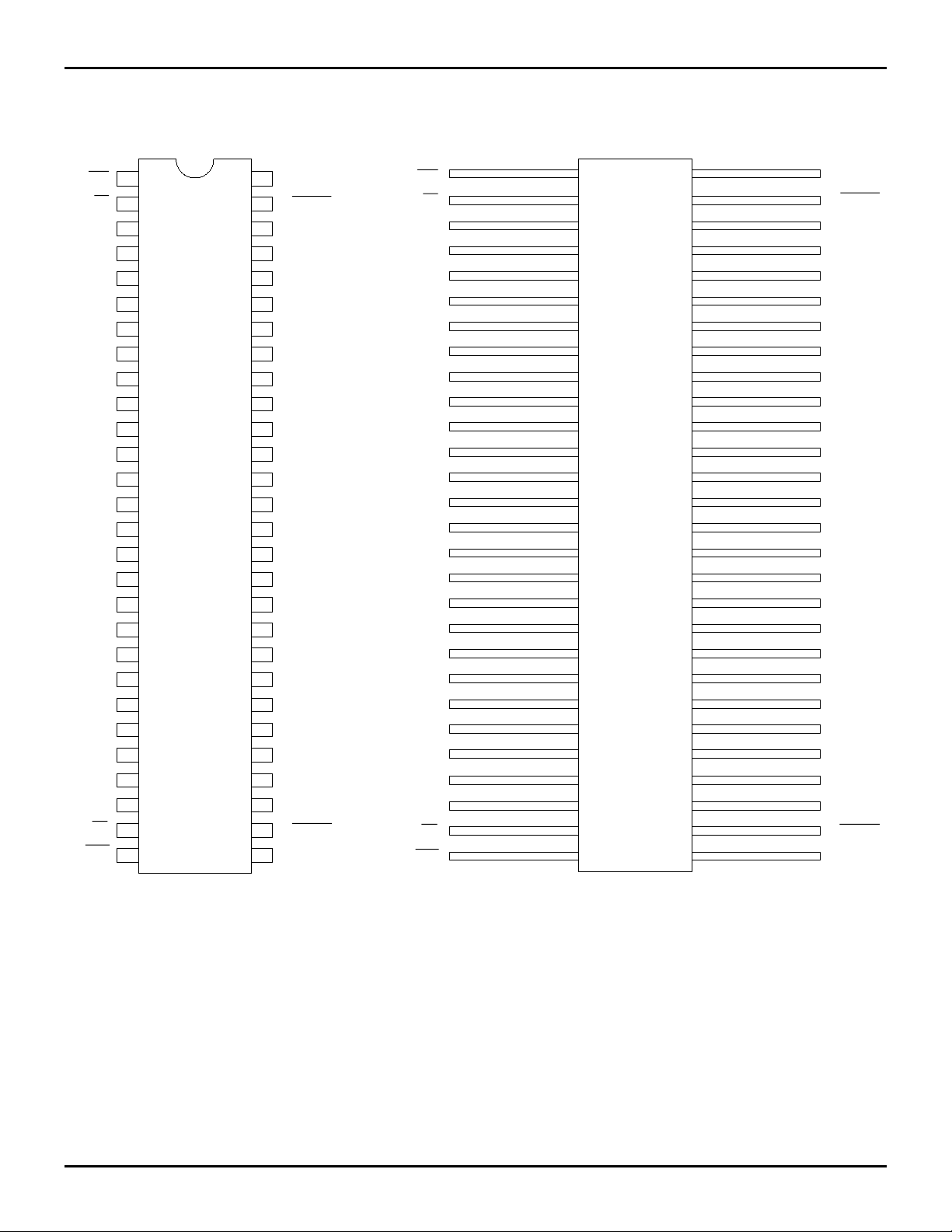
PIN CONFIGURATIONS
1
CLR
1
OE
1Q1
GND
1Q2
Q3
1
VCC
Q4
1
1
Q5
Q6
1
GND
Q7
1
1
Q8
1Q9
Q1
2
Q2
2
2
Q3
GND
2
Q4
Q5
2
2
Q6
V
CC
2Q7
2
Q8
GND
Q9
2
2
OE
2CLR
1
2
3
4
5
6
7
8
9
10
11
12
13
14
15
16
17
18
19
20
21
22
23
24
26
27
28
SO56-1
SO56-2
SO56-3
48
43
56
55
54
53
52
51
50
49
47
46
45
44
42
41
40
39
38
37
36
35
34
33
3225
31
30
29
1CLK
1
CLKEN
1D1
GND
1D2
1
D3
VCC
D4
1
D5
1
1
D6
GND
D7
1
1
D8
D9
1
2D1
2D2
2D3
GND
2D4
2
D5
D6
2
VCC
2D7
D8
2
GND
2
D9
CLKEN
2
CLK
2
CLR
1
1
OE
1
GND
1Q2
1
V
1
1
1
GND
1
1
1Q9
2
2
2
GND
2
2
2
V
2Q7
2
GND
2Q9
2
OE
2
CLR
Q
Q
Q
Q
Q
Q
Q
Q
Q
Q
Q
Q
Q
Q
CC
CC
1
2
1
3
4
5
3
6
7
4
5
6
8
9
10
11
7
8
1
2
3
12
13
14
15
16
17
E56-1
18
4
5
6
19
20
21
22
23
8
24
25
26
27
28
56
55
54
53
52
51
50
49
48
47
46
45
44
43
42
41
40
39
38
37
36
35
34
33
32
31
30
29
CLK
1
1
CLKEN
1D1
GND
1D2
1
D
3
V
CC
1
D
4
1
D
5
1
D
6
GND
1
D
7
1
D
8
1
D
9
2D1
2
D
2
2
D
3
GND
2D4
D
5
2
2
D
6
V
CC
2D7
D
8
2
GND
2
D
9
CLKEN
2
2
CLK
SSOP/
TSSOP/TVSOP
TOP VIEW
CERPACK
TOP VIEW
2772 drw 03 2772 drw 04
5.16 2
IDT54/74FCT16823AT/BT/CT/ET, 162823AT/BT/CT/ET
FAST CMOS 18-BIT REGISTER MILITARY AND COMMERCIAL TEMPERATURE RANGES
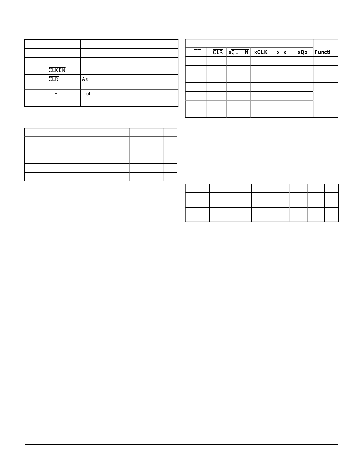
PIN DESCRIPTION
Pin Names Description
xDx Data inputs
xCLK Clock Inputs
x
CLKEN
x
CLR
x
OE
xQx 3-State Outputs
ABSOLUTE MAXIMUM RATINGS
Symbol Description Max. Unit
(2)
VTERM
VTERM
TSTG Storage Temperature –65 to +150 °C
IOUT DC Output Current –60 to +120 mA
NOTES:
1. Stresses greater than those listed under ABSOLUTE MAXIMUM RATINGS may cause permanent damage to the device. This is a stress rating
only and functional operation of the device at these or any other conditions
above those indicated in the operational sections of this specification is
not implied. Exposure to absolute maximum rating conditions for
extended periods may affect reliability.
2. All device terminals except FCT162XXXT Output and I/O terminals.
3. Output and I/O terminals for FCT162XXXT.
Terminal Voltage with Respect to
GND
(3)
Terminal Voltage with Respect to
GND
Clock Enable Inputs (Active LOW)
Asynchronous clear Inputs
(Active LOW)
Output Enable Inputs (Active LOW)
(1)
–0.5 to +7.0 V
–0.5 to
CC +0.5
V
2772 tbl 01
V
2772 lnk 03
FUNCTION TABLE
(1)
Inputs Outputs
x
OEOEx
CLR
CLR
x
CLKEN
CLKEN
xCLK xDx xQx Function
H X X X X Z High Z
L L X X X L Clear
LHHXXQ
(2)
Hold
HH L ↑L Z Load
HH L ↑HZ
LH L ↑LL
LH L ↑HH
NOTES: 2772 tbl 02
1. H = HIGH Voltage Level
L = LOW Voltage Level
X = Don’t Care
Z = High Impedance
2. Output level before indicated steady-state input conditions were established.
CAPACITANCE (TA = +25°C, f = 1.0MHz)
Symbol Parameter
CIN Input
Capacitance
COUT Output
Capacitance
NOTE:
1. This parameter is measured at characterization but not tested.
(1)
Conditions Typ. Max. Unit
VIN = 0V 3.5 6.0 pF
VOUT = 0V 3.5 8.0 pF
2772 lnk 04
5.16 3
 Loading...