

Integrated Device Technology Inc IDT74FCT16H245ATPFB, IDT74FCT16H245ATPF, IDT74FCT16H245ATPAB, IDT74FCT16H245ATPA, IDT74FCT16H245ATEB Datasheet
...
Integrated Device Technology, Inc.
FAST CMOS 16-BIT
BIDIRECTIONAL
TRANSCEIVERS
IDT54/74FCT16245T/AT/CT/ET
IDT54/74FCT162245T/AT/CT/ET
IDT54/74FCT166245T/AT/CT
IDT54/74FCT162H245T/AT/CT/ET
FEATURES:
• Common features:
– 0.5 MICRON CMOS Technology
– High-speed, low-power CMOS replacement for
ABT functions
– Typical t
SK(o) (Output Skew) < 250ps
– Low input and output leakage ≤ 1µA (max.)
– ESD > 2000V per MIL-STD-883, Method 3015;
> 200V using machine model (C = 200pF, R = 0)
– Packages include 25 mil pitch SSOP, 19.6 mil pitch
TSSOP, 15.7 mil pitch TVSOP and 25 mil pitch Cerpack
– Extended commercial range of -40°C to +85°C
• Features for FCT16245T/AT/CT/ET:
– High drive outputs (-32mA IOH, 64mA IOL)
– Power off disable outputs permit “live insertion”
– Typical VOLP (Output Ground Bounce) < 1.0V at
VCC = 5V, TA = 25°C
• Features for FCT162245T/AT/CT/ET:
– Balanced Output Drivers: ±24mA (commercial),
±16mA (military)
– Reduced system switching noise
– Typical VOLP (Output Ground Bounce) < 0.6V at
VCC = 5V,TA = 25°C
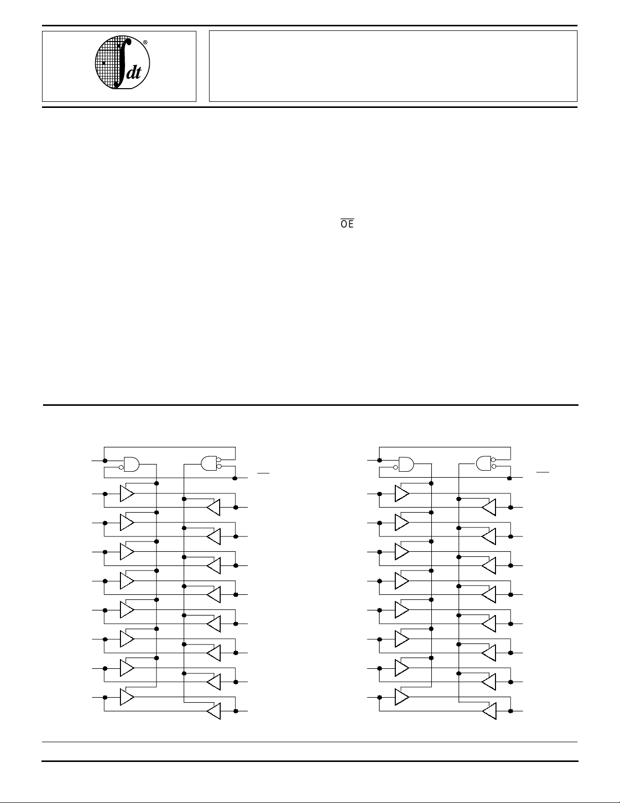
FUNCTIONAL BLOCK DIAGRAM
DESCRIPTION:
The 16-bit transceivers are built using advanced dual metal
CMOS technology. These high-speed, low-power transceivers are ideal for synchronous communication between two
busses (A and B). The Direction and Output Enable controls
operate these devices as either two independent 8-bit transceivers or one 16-bit transceiver. The direction control pin
(xDIR) controls the direction of data flow. The output enable
pin (xOE) overrides the direction control and disables both
ports. All inputs are designed with hysteresis for improved
noise margin.
The FCT16245T are ideally suited for driving high-capacitance loads and low-impedance backplanes. The output buffers are designed with power off disable capability to allow "live
insertion" of boards when used as backplane drivers.
The FCT162245T have balanced output drive with current
limiting resistors. This offers low ground bounce, minimal
undershoot, and controlled output fall times– reducing the
need for external series terminating resistors. The
FCT162245T are plug-in replacements for the FCT16245T
and ABT16245 for on-board interface applications.
The FCT166245T are suited for very low noise, point-topoint driving where there is a single receiver, or a light lumped
1 DIR
1A1
A2
1
A3
1
1
A4
A5
1
A6
1
1
A7
1
A8
The IDT logo is a registered trademark of Integrated Device Technology, Inc.
1OE
1
B1
B2
1
B3
1
1
B4
B5
1
1
B6
1
B7
1
B8
2545 drw 01
2
DIR
2A1
A
2
2
A
2
A
2
A
A
2
2
A
A
2
2
OE
2
B
1
2
2
B
2
3
2
B
3
4
B
4
2
5
2
B
5
6
2
B
6
7
B
7
2
8
B
8
2
2545 drw 02
MILITARY AND COMMERCIAL TEMPERATURE RANGES AUGUST 1996
1996 Integrated Device Technology, Inc. 5.3 DSC-2545/9
1
IDT54/74FCT16245T/AT/CT/ET, 162245T/AT/CT/ET, IDT54/74FCT166245T/AT/CT, IDT54/74FCT162H245T/AT/CT/ET
FAST CMOS 16-BIT BIDIRECTIONAL TRANSCEIVERS MILITARY AND COMMERCIAL TEMPERATURE RANGES
FEATURES: (Cont'd.)
• Features for FCT166245T/AT/CT:
– Light Drive A Port: ±8mA (commercial),
±6mA (military)
– High Drive B Port: +64mA, –32mA (commercial),
+48mA, –24mA (military)
– Minimal system switching noise
– Typical VOLP (Output Ground Bounce) < 0.25V at
VCC = 5V,TA = 25°C (A Port Switching)
• Features for FCT162H245T/AT/CT/ET:
– Bus Hold retains last active bus state during 3-state
– Eliminates the need for external pull up resistors
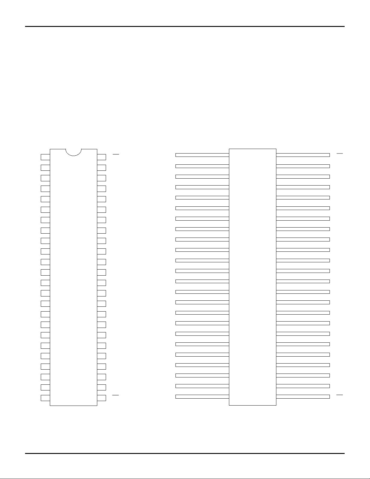
PIN CONFIGURATIONS
1
DIR
1B1
1B2
GND
1B3
1
B
V
CC
1
B
1
B
GND
4
5
6
1
2
3
4
5
6
7
8
9
10
48
47
46
45
44
43
42
41
40
39
1
OE
1A1
1
A
2
GND
1A3
1
A
4
V
CC
1
A
5
1
A
6
GND
1DIR
1B1
1B2
GND
1B3
B4
1
VCC
B5
1
1
B6
GND
DESCRIPTION: (Cont'd.)
load (<100pF). The buffers are designed to limit the output
current to levels which will avoid noise and ringing on the
signal lines without using external series terminating resistors. These parts have a ±8mA driver on the "A" Port and a
+64/–32mA driver on the "B" Port, making them ideal for
interfacing noisy system busses to noise sensitive interfaces.
The FCT162H245T have "Bus Hold" which retains the
input's last state whenever the input goes to high impedance.
This prevents "floating" inputs and eliminates the need for
pull-up/down resistors.
1
2
3
4
5
6
7
8
9
10
48
47
46
45
44
43
42
41
40
39
1OE
1A1
1
A2
GND
1A3
1
A4
VCC
1
A5
1
A6
GND
1
B
1
B
2
B
2B2
GND
2
B
B
2
V
CC
2
B
B
2
GND
2
B
2
B
2
DIR
1
7
8
11
12
SO48-1
38
37
1
A
7
1
A
8
SO48-2
1
3
4
5
6
7
8
13
14
15
16
17
18
19
20
21
22
23
24
SO48-3
36
35
34
33
32
31
30
29
28
27
26
25
2
A
1
2
A
2
GND
2
A
3
A
4
2
V
CC
2
A
5
A
6
2
GND
2
A
7
2
A
8
2
OE
2545 drw 03
B7
1
B8
2
B1
2B2
GND
B3
2
B4
2
CC
V
B5
2
2
B6
GND
B7
2
2
B8
DIR
2
SSOP/
TSSOP/TVSOP
TOP VIEW
11
12
13
14
15
16
17
18
19
20
21
22
23
24
CERPACK
TOP VIEW
E48-1
38
37
36
35
34
33
32
31
30
29
28
27
26
25
2545 drw 04
1
A7
1
A8
2
A1
2
A2
GND
A3
2
A4
2
VCC
2
A5
2
A6
GND
A7
2
2
A8
2OE
5.3 2
IDT54/74FCT16245T/AT/CT/ET, 162245T/AT/CT/ET, IDT54/74FCT166245T/AT/CT, IDT54/74FCT162H245T/AT/CT/ET
FAST CMOS 16-BIT BIDIRECTIONAL TRANSCEIVERS MILITARY AND COMMERCIAL TEMPERATURE RANGES
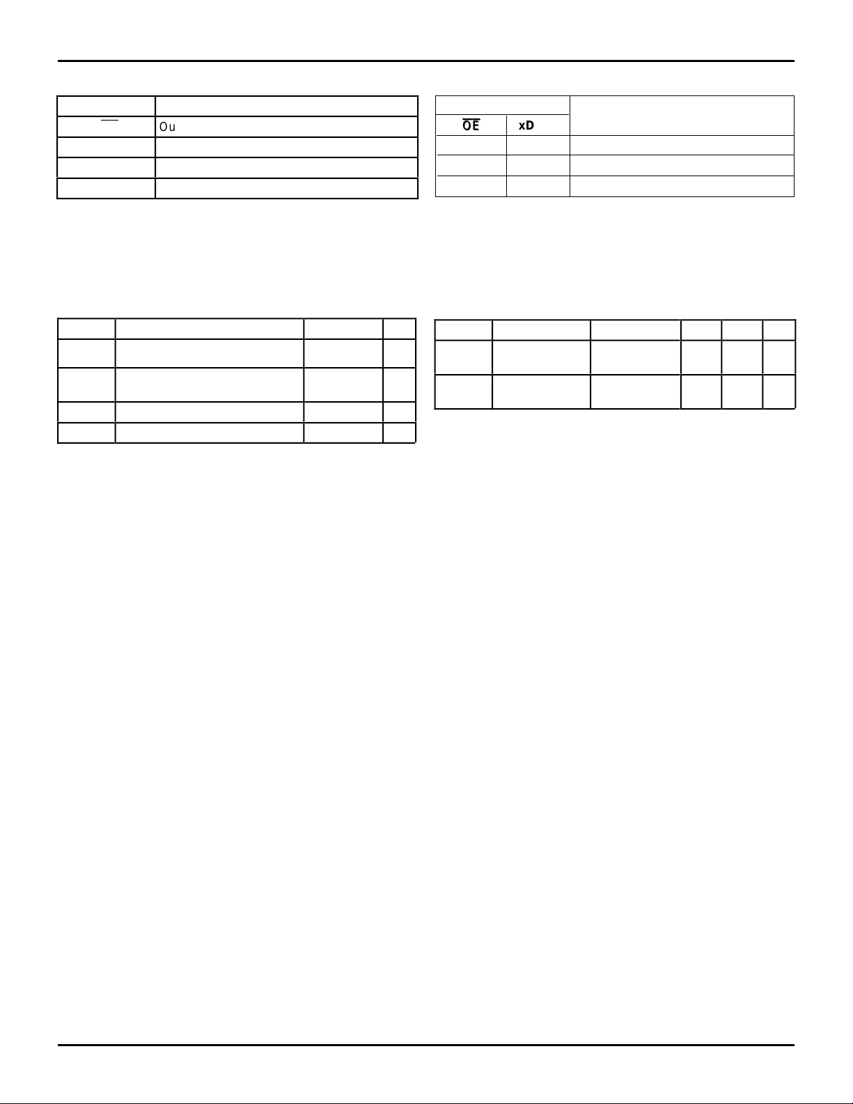
PIN DESCRIPTION
Pin Names Description
x
OE
xDIR Direction Control Input
xAx Side A Inputs or 3-State Outputs
xBx Side B Inputs or 3-State Outputs
NOTES:
1. On FCT162H245T these pins have “Bus Hold”. All other pins are standard
inputs, outputs or I/Os.
2. On FCT166245T this is the ±8mA Port.
3. On FCT166245T this is the +64/–32mA Port.
ABSOLUTE MAXIMUM RATINGS
Symbol Description Max. Unit
(2)
VTERM
(3)
VTERM
TSTG Storage Temperature –65 to +150 °C
IOUT DC Output Current –60 to +120 mA
NOTES:
1. Stresses greater than those listed under ABSOLUTE MAXIMUM RATINGS may cause permanent damage to the device. This is a stress rating
only and functional operation of the device at these or any other conditions
above those indicated in the operational sections of this specification is
not implied. Exposure to absolute maximum rating conditions for
extended periods may affect reliability.
2. All device terminals except FCT162XXXT and FCT166XXXT (A-Port)
Output and I/O terminals.
3. Output and I/O terminals for FCT162XXXT and FCT166XXXT (A-Port).
Output Enable Input (Active LOW)
Terminal Voltage with Respect to
GND
Terminal Voltage with Respect to
GND
(1,2)
(1,3)
2545 tbl 01
(1)
–0.5 to +7.0 V
–0.5 to
CC +0.5
V
2545 lnk 03
V
FUNCTION TABLE
(1)
Inputs
x
OE
OE
xDIR Outputs
L L Bus B Data to Bus A
L H Bus A Data to Bus B
H X High Z State
NOTE:
1. H = HIGH Voltage Level
L = LOW Voltage Level
X = Don't Care
Z = High Impedance
CAPACITANCE (TA = +25°C, f = 1.0MHz)
Symbol Parameter
CIN Input
Capacitance
CI/O I/O
Capacitance
NOTE:
1. This parameter is measured at characterization but not tested.
(1)
Conditions Typ. Max. Unit
VIN = 0V 3.5 6.0 pF
VOUT = 0V 3.5 8.0 pF
2545 tbl 02
2545 lnk 04
5.3 3
 Loading...