

Integrated Device Technology Inc IDT74FCT16H244TPA, IDT74FCT16H244TEB, IDT74FCT16H244TE, IDT74FCT16H244ETPVB, IDT74FCT16H244ETPV Datasheet
...
Integrated Device Technology, Inc.
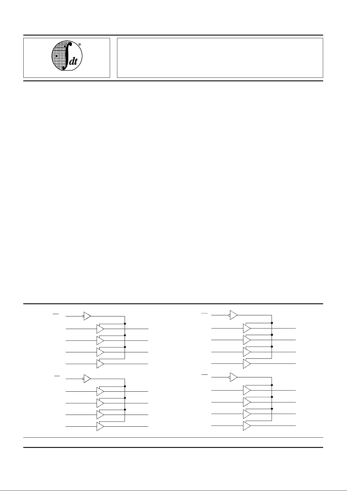
FUNCTIONAL BLOCK DIAGRAM
1Y1
1
Y2
1
Y3
1
Y4
1
A1
1A2
1
A3
1
A4
2OE
2A1
2A2
2
A3
2
A4
2
Y1
2
Y2
2
Y3
2
Y4
2544 drw 01
1OE
3OE
3A1
3
A2
3
A3
3
A4
3
Y1
3Y2
3
Y3
3
Y4
4OE
4A1
4
A2
4
A3
4
A4
4Y1
4
Y2
4
Y3
4
Y4
2544 drw 02
The IDT logo is a registered trademark of Integrated Device Technology, Inc.
MILITARY AND COMMERCIAL TEMPERATURE RANGES OCTOBER 1996
1996 Integrated Device Technology, Inc. 5.2 DSC-2544/9
15
FAST CMOS 16-BIT
BUFFER/LINE DRIVER
IDT54/74FCT16244T/AT/CT/ET
IDT54/74FCT162244T/AT/CT/ET
IDT54/74FCT166244T/AT/CT
IDT54/74FCT162H244T/AT/CT/ET
FEATURES:
• Common features:
– 0.5 MICRON CMOS Technology
– High-speed, low-power CMOS replacement for
ABT functions
– Typical tSK(o) (Output Skew) < 250ps
– Low input and output leakage ≤ 1µA (max.)
– ESD > 2000V per MIL-STD-883, Method 3015;
> 200V using machine model (C = 200pF, R = 0)
– Packages include 25 mil pitch SSOP, 19.6 mil pitch
TSSOP, 15.7 mil pitch TVSOP and 25 mil pitch Cerpack
– Extended commercial range of -40°C to +85°C
• Features for FCT16244T/AT/CT/ET:
– High drive outputs (-32mA I
OH, 64mA IOL)
– Power off disable outputs permit “live insertion”
– Typical VOLP (Output Ground Bounce) < 1.0V at
VCC = 5V, TA = 25°C
• Features for FCT162244T/AT/CT/ET:
– Balanced Output Drivers: ±24mA (commercial),
±16mA (military)
– Reduced system switching noise
– Typical VOLP (Output Ground Bounce) < 0.6V at
VCC = 5V,TA = 25°C
• Features for FCT166244T/AT/CT:
– Light Drive Balanced Output: ±8mA (commercial),
±6mA (military)
– Minimal system switching noise
– Typical VOLP (Output Ground Bounce) < 0.25V at
V
CC = 5V,TA = 25°C
• Features for FCT162H244T/AT/CT/ET:
– Bus-Hold retains last active bus state during 3-state
– Eliminates the need for external pull up resistors
DESCRIPTION:
The 16-Bit Buffer/Line Driver is for bus interface or signal buffering
applications requiring high speed and low power dissipation. These
devices have a flow through pin organization, and shrink packaging
to simplify board layout. All inputs are designed with hysteresis for
improved noise margin. The three-state controls allow independent
4-bit, 8-bit or combined 16-bit operation. These parts are plug in
replacements for 54/74ABT16244 where higher speed, lower noise
or lower power dissipation levels are desired.
The FCT16244T/AT/CT/ET are ideally suited for driving
high capacitance loads (>200pF) and low impedance
backplanes. These "high drive" buffers are designed with
power off disable capability to allow "live insertion" of boards
when used in a backplane interface.
The FCT162244T/AT/CT/ET have balanced output current
levels and current limiting resistors. These offer low ground
bounce, minimal undershoot, and controlled output fall times,
reducing the need for external series terminating resistors
while still providing very high speed operation for loads of less
than 200pF.
The FCT166244T/AT/CT are suited for very low noise,
point-to-point driving where there is a single receiver, or a very
light lumped load (<100pF). The buffers are designed to limit
the output current to levels which will avoid noise and ringing
on the signal lines without using external series terminating
resistors.
The FCT162H244T/AT/CT/ET have "Bus-Hold" which retains the input's last state whenever the input goes to high
impedance. This prevents "floating" inputs and eliminates the
need for pull-up/down resistors.

IDT54/74FCT16244T/AT/CT/ET, 162244T/AT/CT/ET,
166244T/AT/CT, 162H244T/AT/CT/ET FAST CMOS 16-BIT BUFFER/LINE DRIVER MILITARY AND COMMERCIAL TEMPERATURE RANGES
5.2 2
PIN CONFIGURATIONS
1Y1
GND
1Y3
VCC
1
OE
GND
3Y2
GND
V
CC
GND
1Y2
1
Y4
2
Y1
2
Y2
2
Y3
2
Y4
3
Y1
3
Y3
3
Y4
4
Y1
4
Y3
4
Y4
4
Y2
4OE
1A1
1
A2
GND
1A3
1
A4
VCC
2
A1
2
A2
2
A3
2
A4
3
A1
3
A2
3
A3
3
A4
VCC
4
A1
4
A3
4
A4
4
A2
GND
GND
GND
2OE
3OE
39
29
30
31
32
33
34
35
36
37
38
25
26
27
28
48
47
41
42
43
44
45
46
40
1
2
3
4
5
6
7
8
9
10
12
13
14
15
16
17
18
19
20
11
21
22
23
24
2544 drw 04
CERPACK
TOP VIEW
E48-1
PIN DESCRIPTION
2544 tbl 01
NOTE:
1. On FCT16xH these pins have “Bus-hold”. All other pins are standard
inputs, outputs or I/Os.
Pin Names Description
x
OE
3–State Output Enable Inputs (Active LOW)
xAx Data Inputs
(1)
xYx 3-State Outputs
1Y1
GND
1Y3
VCC
GND
3Y2
GND
V
CC
GND
1Y2
1
Y4
2
Y1
2
Y2
2
Y3
2
Y4
3
Y1
3
Y3
3
Y4
4
Y1
4
Y3
4
Y4
4
Y2
4OE
1A1
1
A2
GND
1A3
1
A4
VCC
2
A1
2
A2
2
A3
2
A4
3
A1
3
A2
3
A3
3
A4
VCC
4
A1
4
A3
4
A4
4
A2
GND
GND
GND
2OE
3OE
2544 drw 03
39
29
30
31
32
33
34
35
36
37
38
25
26
27
28
48
47
41
42
43
44
45
46
40
1
2
3
4
5
6
7
8
9
10
12
13
14
15
16
17
18
19
20
11
21
22
23
24
SSOP/
TSSOP/TVSOP
TOP VIEW
SO48-1
SO48-2
SO48-3
1OE
5.2 3
IDT54/74FCT16244T/AT/CT/ET, 162244T/AT/CT/ET,
166244T/AT/CT, 162H244T/AT/CT/ET FAST CMOS 16-BIT BUFFER/LINE DRIVER MILITARY AND COMMERCIAL TEMPERATURE RANGES
NOTE:
1. This parameter is measured at characterization but not tested.
CAPACITANCE (TA = +25°C, f = 1.0MHz)
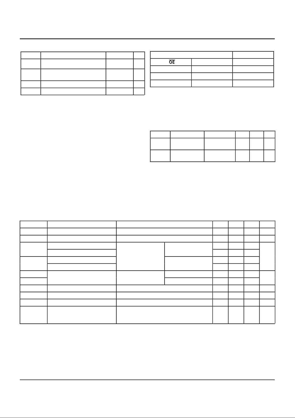
FUNCTION TABLE
(1)
2544 lnk 04
NOTE:
1. H = HIGH Voltage Level
X = Don’t Care
L = LOW Voltage Level
Z = High Impedance
2544 tbl 02
Symbol Parameter
(1)
Conditions Typ. Max. Unit
C
IN
Input
Capacitance
VIN = 0V 3.5 6.0
pF
C
OUT
Output
Capacitance
V
OUT
= 0V 3.5 8.0
pF
ABSOLUTE MAXIMUM RATINGS
(1)
DC ELECTRICAL CHARACTERISTICS OVER OPERATING RANGE (STANDARD PARTS)
Following Conditions Apply Unless Otherwise Specified:
Commercial: TA = –40°C to +85°C, VCC = 5.0V ± 10%; Military: TA = –55°C to +125°C, VCC = 5.0V ± 10%
Inputs Outputs
x
OEOE xAx xYx
LLL
LHH
HXZ
Symbol Parameter Test Conditions
(1)
Min. Typ.
(2)
Max. Unit
VIH Input HIGH Level Guaranteed Logic HIGH Level 2.0 — — V
VIL Input LOW Level Guaranteed Logic LOW Level — — 0.8 V
II H Input HIGH Current (Input pins)
(5)
VCC = Max. VI = VCC — — ±1 µA
Input HIGH Current (I/O pins)
(5)
— — ±1
II L Input LOW Current (Input pins)
(5)
VI = GND — — ±1
Input LOW Current (I/O pins)
(5)
— — ±1
IOZH High Impedance Output Current VCC = Max. VO = 2.7V — — ±1 µA
IOZL (3-State Output pins)
(5)
VO = 0.5V — — ±1
VIK Clamp Diode Voltage VCC = Min., IIN = –18mA — –0.7 –1.2 V
IOS Short Circuit Current VCC = Max., VO = GND
(3)
–80 –140 –225 mA
VH Input Hysteresis — — 100 — mV
ICCL
ICCH
ICCZ
Quiescent Power Supply Current VCC = Max., VIN = GND or VCC — 5 500 µA
2544 lnk 05
NOTES:
1. For conditions shown as Max. or Min., use appropriate value specified under Electrical Characteristics for the applicable device type.
2. Typical values are at Vcc = 5.0V, +25°C ambient.
3. Not more than one output should be tested at one time. Duration of the test should not exceed one second.
4. Duration of the condition can not exceed one second.
5. The test limit for this parameter is ± 5µA at T
A = –55°C.
Symbol Description Max. Unit
VTERM
(2)
Terminal Voltage with Respect to
GND
–0.5 to +7.0 V
VTERM
(3)
Terminal Voltage with Respect to
GND
–0.5 to
V
CC +0.5
V
TSTG Storage Temperature –65 to +150 °C
IOUT DC Output Current –60 to +120 mA
NOTES:
1. Stresses greater than those listed under ABSOLUTE MAXIMUM RATINGS
may cause permanent damage to the device. This is a stress rating only
and functional operation of the device at these or any other conditions
above those indicated in the operational sections of this specification is
not implied. Exposure to absolute maximum rating conditions for
extended periods may affect reliability.
2. All device terminals except FCT162XXXT and FCT166XXXT output and
I/O terminals.
3. Output and I/O terminals for FCT162XXXT and FCT166XXXT.
2544 lnk 03
 Loading...