

Integrated Device Technology Inc IDT74FCT16601ETPV, IDT74FCT16601ETPF, IDT74FCT16601ETPA, IDT74FCT16601CTPV, IDT74FCT16601CTPF Datasheet
...
Integrated Device Technology, Inc.
FAST CMOS
18-BIT UNIVERSAL BUS
TRANSCEIVER
WITH 3-STATE OUTPUTS
IDT74FCT16601AT/CT/ET
IDT74FCT162601AT/CT/ET
PRODUCT PREVIEW
FEATURES:
• Common features:
– 0.5 MICRON CMOS Technology
– High-speed, low-power CMOS replacement for
ABT functions
– Typical tSK(o) (Output Skew) < 250ps
– Low input and output leakage ≤1µA (max.)
– ESD > 2000V per MIL-STD-883, Method 3015;
> 200V using machine model (C = 200pF, R = 0)
– Packages include 25 mil pitch SSOP, 19.6 mil pitch
TSSOP, 15.7 mil pitch TVSOP and 25 mil pitch Cerpack
– Extended commercial range of -40°C to +85°C
–V
CC = 5V ±10%
• Features for FCT16601AT/CT/ET:
– High drive outputs (-32mA IOH, 64mA IOL)
– Power off disable outputs permit “live insertion”
– Typical VOLP (Output Ground Bounce) < 1.0V at
VCC = 5V, TA = 25°C
• Features for FCT162601AT/CT/ET:
– Balanced Output Drivers: ±24mA
– Reduced system switching noise
– Typical VOLP (Output Ground Bounce) < 0.6V at
VCC = 5V,TA = 25°C
DESCRIPTION:
The FCT16601AT/CT/ET and FCT162601AT/CT/ET 18-
bit registered transceivers are built using advanced dual metal
CMOS technology. These high-speed, low-power 18-bit registered bus transceivers combine D-type latches and D-type
flip-flops to allow data flow in either direction in a transparent,
latched or clocked mode. Each direction has an independent
latch enable, an independent clock with a clock enable, and an
independent output enable. The package is organized with a
flow-through signal pin organization to ease board layout. All
inputs are designed with hysteresis for improved noise margin.
This transceiver is ideally suited for high speed memory
interfaces which utilize high speed synchronous writes, by
clocking the data into a high speed register. Reads can then
be performed in a transparent or latched mode utilizing the
same transceiver.
The FCT16601AT/CT/ET are ideally suited for driving
high-capacitance loads and low-impedance backplanes. The
output buffers are designed with power off disable capability
to allow "live insertion" of boards when used as backplane
drivers.
The FCT162601AT/CT/ET have balanced output drive
with current limiting resistors. This offers low ground bounce,
minimal undershoot, and controlled output fall times–reducing
the need for external series terminating resistors. The
FCT162601AT/CT/ET are plug-in replacements for the
FCT16601AT/CT/ET and ABT16601 for on-board bus interface applications.
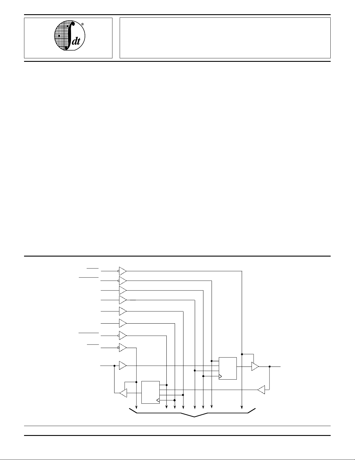
FUNCTIONAL BLOCK DIAGRAM
OEAB
CLKENAB
CLKAB
LEAB
LEBA
CLKBA
CLKENBA
OEBA
The IDT logo is a registered trademark of Integrated Device Technology, Inc.
COMMERCIAL TEMPERATURE RANGE AUGUST 1996
1996 Integrated Device Technology, Inc. 5.9 DSC-3247/-
1
56
55
2
28
30
29
27
PRODUCT PREVIEW
A1
3
CE
1D
C1
CLK
TO 17 OTHER CHANNELS
CE
1D
C1
CLK
54
B1
3247 drw 01
1
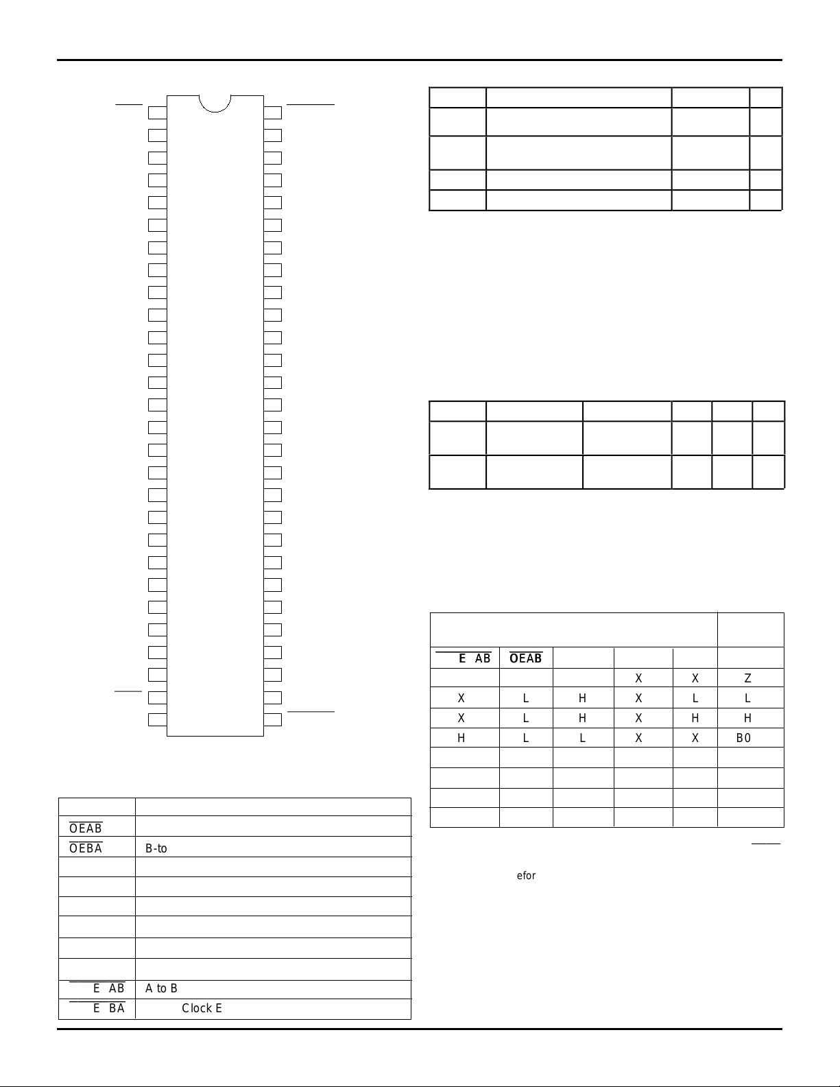
IDT74FCT16601AT/CT/ET, 162601AT/CT/ET
FAST CMOS 18-BIT UNIVERSAL BUS TRANSCEIVERS COMMERCIAL TEMPERATURE RANGE
PIN CONFIGURATIONS
OEAB
LEAB
A
GND
A
A
V
CC
A
A
A
GND
A
A
A
10
A
A
11
A
12
GND
A
13
A
14
15
A
V
CC
A
16
17
A
GND
A
18
OEBA
LEBA
1
2
3
4
5
6
7
8
9
1
2
3
4
5
6
7
8
9
10
11
12
13
14
SO56-1
SO56-2
15
SO56-3
16
17
18
19
20
21
22
23
24
26
27
28
SSOP/
TSSOP/TVSOP
TOP VIEW
56
55
54
53
52
51
50
49
48
47
46
45
44
43
42
41
40
39
38
37
36
35
34
33
3225
31
30
29
CLKENAB
CLKAB
B
1
GND
B
2
B
3
V
CC
B
4
B
5
B
6
GND
B
7
B
8
B
9
B
10
B
11
B
12
GND
B
13
B
14
B
15
V
CC
B
16
B
17
GND
18
B
CLKBA
CLKENBA
3247 drw 02
PIN DESCRIPTION
Pin Names Description
OEAB
OEBA
A-to-B Output Enable Input (Active LOW)
B-to-A Output Enable Input (Active LOW)
LEAB A-to-B Latch Enable Input
LEBA B-to-A Latch Enable Input
CLKAB A-to-B Clock Input
CLKBA B-to-A Clock Input
Ax A-to-B Data Inputs or B-to-A 3-State Outputs
Bx B-to-A Data Inputs or A-to-B 3-State Outputs
CLKENAB
CLKENBA
A to B Clock Enable Input
B to A Clock Enable Input
PRODUCT PREVIEW
3247 tbl 01
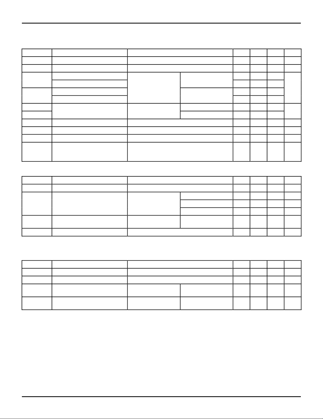
ABSOLUTE MAXIMUM RATINGS
(1)
Symbol Description Max. Unit
Terminal Voltage with Respect to
(2)
V
TERM
V
TERM
T
STG
I
OUT
NOTES:
1. Stresses greater than those listed under ABSOLUTE MAXIMUM RATINGS may cause permanent damage to the device. This is a stress rating
only and functional operation of the device at these or any other conditions
above those indicated in the operational sections of this specification is
not implied. Exposure to absolute maximum rating conditions for
extended periods may affect reliability.
2. All device terminals except FCT162XXXT Output and I/O terminals.
3. Output and I/O terminals for FCT162XXXT.
GND
Terminal Voltage with Respect to
(3)
GND
Storage Temperature –65 to +150°C
DC Output Current –60 to +120 mA
–0.5 to +7.0 V
–0.5 to
V
CC
+0.5
3247 lnk 03
V
CAPACITANCE (TA = +25°C, f = 1.0MHz)
Symbol Parameter
CIN Input
Capacitance
CI/O I/O
Capacitance
NOTE:
1. This parameter is measured at characterization but not tested.
FUNCTION TABLE
CLKENAB
CLKENAB
XHXXXZ
XLHXLL
XLHXHH
HLLXXB0
LLL↑LL
LLL↑HH
LLLLXB0
LLLHXB0
NOTES: 3247 tbl 02
1. A-to-B data flow is shown. B-to-A data flow is similar but uses
LEBA and CLKBA.
2. Output level before the indicated steady-state input conditions were
established.
3. Output level before the indicated steady-state input conditions were
established, provided that CLKAB was HIGH before LEAB went LOW.
4. H = HIGH Voltage Level
L = LOW Voltage Level
X = Don't Care
Z = High-impedance
↑ = LOW-to-HIGH Transition
OEAB
OEAB
(1)
Conditions Typ. Max. Unit
VIN = 0V 3.5 6.0 pF
VOUT = 0V 3.5 8.0 pF
3247 lnk 04
(1,4)
Inputs Outputs
LEAB CLKAB A B
(2)
(2)
(3)
OEBA
,
5.9 2
IDT74FCT16601AT/CT/ET, 162601AT/CT/ET
FAST CMOS 18-BIT UNIVERSAL BUS TRANSCEIVERS COMMERCIAL TEMPERATURE RANGE
DC ELECTRICAL CHARACTERISTICS OVER OPERATING RANGE
Following Conditions Apply Unless Otherwise Specified:
Commercial: TA = –40°C to +85°C, VCC = 5.0V ± 10%
Symbol Parameter Test Conditions
(1)
Min. Typ.
VIH Input HIGH Level Guaranteed Logic HIGH Level 2.0 — — V
VIL Input LOW Level Guaranteed Logic LOW Level — — 0.8 V
II H Input HIGH Current (Input pins) VCC = Max. VI = VCC — — ±1 µA
Input HIGH Current (I/O pins) — — ±1
II L Input LOW Current (Input pins) VI = GND — — ±1
Input LOW Current (I/O pins) — — ±1
IOZH High Impedance Output Current VCC = Max. VO = 2.7V — — ±1 µA
IOZL (3-State Output pins) VO = 0.5V — — ±1
VIK Clamp Diode Voltage VCC = Min., IIN = –18mA — –0.7 –1.2 V
IOS Short Circuit Current VCC = Max., VO = GND
(3)
–80 –140 –225 mA
VH Input Hysteresis — — 100 — mV
ICCL
Quiescent Power Supply Current VCC = Max., VIN = GND or VCC — 5 500 µA
ICCH
ICCZ
(2)
Max. Unit
3247 lnk 05
OUTPUT DRIVE CHARACTERISTICS FOR FCT16601T
Symbol Parameter Test Conditions
I
O
V
OH
Output Drive Current VCC = Max., VO = 2.5V
Output HIGH Voltage VCC = Min. IOH = –3mA 2.5 3.5 — V
VIN = V
IH
or V
IL
(3)
IOH = –15mA 2.4 3.5 — V
IOH = –32mA
V
I
OL
OFF
Output LOW Voltage VCC = Min.
IN
= V
IH
V
or V
Input/Output Power Off Leakage VCC = 0V, V
IN
I
OL
= 64mA — 0.2 0.55 V
IL
or V
O
≤ 4.5V — —
(1)
(4)
Min. Typ.
–50
2.0 3.0 — V
(2)
Max. Unit
—–
180 mA
±
1
µ
A
OUTPUT DRIVE CHARACTERISTICS FOR FCT162601T
Symbol Parameter Test Conditions
IODL Output LOW Current VCC = 5V, VIN = VIH or VIL, VOUT = 1.5V
IODH Output HIGH Current VCC = 5V, VIN = VIH or V IL, VOUT = 1.5V
VOH Output HIGH Voltage VCC = Min.
V
IN = VIH or VIL
VOL Output LOW Voltage VCC = Min.
V
IN = VIH or VIL
NOTES:
1. For conditions shown as Max. or Min., use appropriate value specified under Electrical Characteristics for the applicable device type.
2. Typical values are at Vcc = 5.0V, +25°C ambient.
3. Not more than one output should be tested at one time. Duration of the test should not exceed one second.
4. Duration of the condition can not exceed one second.
PRODUCT PREVIEW
(1)
(3)
(3)
Min. Typ.
60 115 200 mA
–60 –115 –200 mA
IOH = –24mA 2.4 3.3 — V
IOL = 24mA — 0.3 0.55 V
(2)
3247 lnk 06
Max. Unit
3247 lnk 07
5.9 3
 Loading...