

Integrated Device Technology Inc IDT74FCT16543TPVB, IDT74FCT16543TPV, IDT74FCT16543TPFB, IDT74FCT16543TPAB, IDT74FCT16543TPA Datasheet
...
Integrated Device Technology, Inc.
FAST CMOS
16-BIT LATCHED
TRANSCEIVER
IDT54/74FCT16543T/AT/CT/ET
IDT54/74FCT162543T/AT/CT/ET
FEATURES:
• Common features:
– 0.5 MICRON CMOS Technology
– High-speed, low-power CMOS replacement for
ABT functions
– Typical tSK(o) (Output Skew) < 250ps
– Low input and output leakage ≤1µA (max.)
– ESD > 2000V per MIL-STD-883, Method 3015;
> 200V using machine model (C = 200pF, R = 0)
– Packages include 25 mil pitch SSOP, 19.6 mil pitch
TSSOP, 15.7 mil pitch TVSOP and 25 mil pitch Cerpack
– Extended commercial range of -40°C to +85°C
–V
CC = 5V ±10%
• Features for FCT16543T/AT/CT/ET:
– High drive outputs (-32mA IOH, 64mA IOL)
– Power off disable outputs permit “live insertion”
– Typical VOLP (Output Ground Bounce) < 1.0V at
VCC = 5V, TA = 25°C
• Features for FCT162543T/AT/CT/ET:
– Balanced Output Drivers: ±24mA (commercial),
±16mA (military)
– Reduced system switching noise
– Typical VOLP (Output Ground Bounce) < 0.6V at
VCC = 5V,TA = 25°C
DESCRIPTION:
The FCT16543T/AT/CT/ET and FCT162543T/AT/CT/ET
16-bit latched transceivers are built using advanced dual metal
CMOS technology. These high-speed, low-power devices are
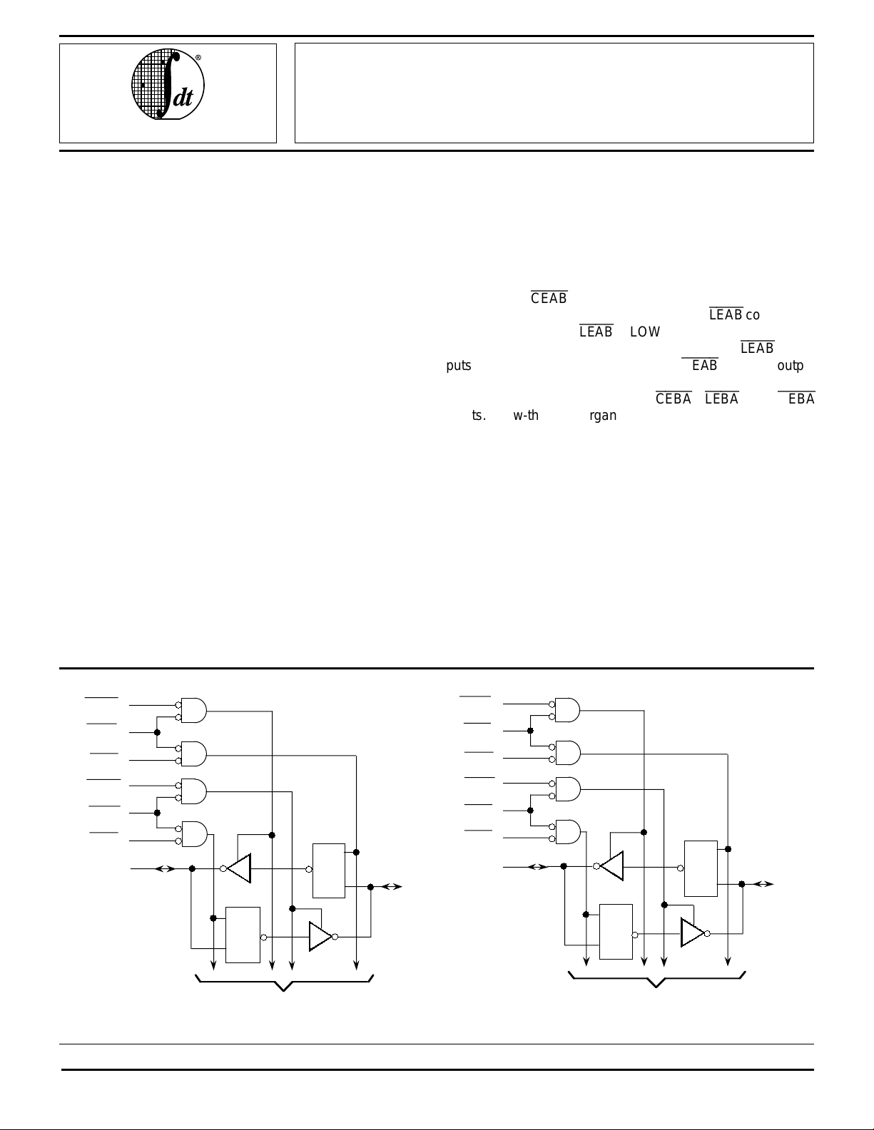
organized as two independent 8-bit D-type latched transceivers with separate input and output control to permit independent control of data flow in either direction. For example, the Ato-B Enable (x
the A port or to output data from the B port. x
latch function. When x
ent. A subsequent LOW-to-HIGH transition of x
puts the A latches in the storage mode. x
enable function on the B port. Data flow from the B port to the
A port is similar but requires using x
inputs. Flow-through organization of signal pins simplifies
layout. All inputs are designed with hysteresis for improved
noise margin.
The FCT16543T/AT/CT/ET are ideally suited for driving
high-capacitance loads and low-impedance backplanes. The
output buffers are designed with power off disable capability to
allow "live insertion" of boards when used as backplane drivers.
The FCT162543T/AT/CT/ET have balanced output drive
with current limiting resistors. This offers low ground bounce,
minimal undershoot, and controlled output fall times–reducing
the need for external series terminating resistors. The
FCT162543T/AT/CT/ET are plug-in replacements for the
FCT16543T/AT/CT/ET and 54/74ABT16543 for on-board bus
interface applications.
CEAB
) must be LOW in order to enter data from
LEAB
LEAB
is LOW, the latches are transpar-
OEAB
performs output
CEBA
, x
LEBA
controls the
LEAB
signal
, and x
OEBA
FUNCTIONAL BLOCK DIAGRAM
1
OEBA
1
CEBA
1
LEBA
1
OEAB
1
CEAB
1
LEAB
1A1
C
D
TO 7 OTHER CHANNELS
The IDT logo is a registered trademark of Integrated Device Technology, Inc.
C
D
1B1
2618 drw 01
MILITARY AND COMMERCIAL TEMPERATURE RANGES SEPTEMBER 1996
1996 Integrated Device Technology, Inc. 5.12 DSC-2618/7
2OEBA
2CEBA
2LEBA
2OEAB
2CEAB
2
LEAB
2A1
C
D
C
D
TO 7 OTHER CHANNELS
B1
2
2618 drw 02
1
IDT54/74FCT16543T/AT/CT/ET, 162543T/AT/CT/ET
FAST CMOS 16-BIT LATCHED TRANSCEIVER MILITARY AND COMMERCIAL TEMPERATURE RANGES
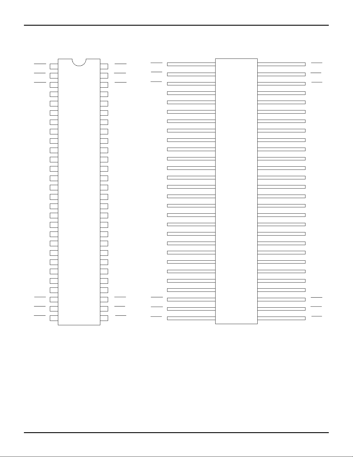
PIN CONFIGURATIONS
1
OEAB
1
LEAB
1
CEAB
GND
GND
GND
GND
2
CEAB
2
LEAB
OEAB
2
1A1
1
V
1
1
1A5
1
1
1
2A1
2
2
2
2
2
V
2
2A8
A
CC
A
A
A
A
A
A
A
A
A
A
CC
A
1OEAB
1LEAB
1CEAB
GND
1A1
1
A2
VCC
1
A3
1
A4
1A5
GND
A6
1
1
A7
1
A8
2A1
2
A2
A3
2
GND
A4
2
2
A5
A6
2
VCC
2
A7
2A8
GND
2CEAB
2LEAB
2OEAB
48
43
56
55
54
53
52
51
50
49
47
46
45
44
42
41
40
39
38
37
36
35
34
33
3225
31
30
29
1
OEBA
1
LEBA
1
CEBA
GND
1B1
B
2
1
V
CC
1B3
1
B
4
1
B
5
GND
B
6
1
1B7
1
B
8
2
B
1
B
2
2
2B3
GND
B
4
2
2
B
5
2
B
6
V
CC
2B7
2
B
8
GND
2
CEBA
2
LEBA
2
OEBA
1
2
3
4
5
2
6
7
3
4
8
9
10
11
6
7
8
2
3
12
13
14
15
16
17
SO56-1
SO56-2
SO56-3
18
4
5
6
19
20
21
22
7
23
24
26
27
28
1
2
3
4
5
6
7
8
9
10
11
12
13
14
15
16
17
18
19
20
21
22
23
24
26
27
28
E56-1
56
55
54
53
52
51
50
49
48
47
46
45
44
43
42
41
40
39
38
37
36
35
34
33
3225
31
30
29
OEBA
1
1LEBA
1CEBA
GND
B1
1
1
B2
VCC
1B3
1
B4
1
B5
GND
B6
1
1B7
1
B8
2
B1
2
B2
2B3
GND
B4
2
2
B5
2
B6
VCC
2B7
2
B8
GND
2CEBA
2LEBA
2OEBA
SSOP/
TSSOP/TVSOP
TOP VIEW
2618 drw 03
CERPACK
2618 drw 04
TOP VIEW
5.12 2
IDT54/74FCT16543T/AT/CT/ET, 162543T/AT/CT/ET
FAST CMOS 16-BIT LATCHED TRANSCEIVER MILITARY AND COMMERCIAL TEMPERATURE RANGES
PIN DESCRIPTION
Pin Names Description
x
OEAB
x
OEBA
x
CEAB
x
CEBA
x
LEAB
x
LEBA
xAx A-to-B Data Inputs or B-to-A 3-State Outputs
xBx B-to-A Data Inputs or A-to-B 3-State Outputs
ABSOLUTE MAXIMUM RATINGS
Symbol Description Max. Unit
(2)
VTERM
(3)
VTERM
TSTG Storage Temperature –65 to +150 °C
IOUT DC Output Current –60 to +120 mA
NOTES:
1. Stresses greater than those listed under ABSOLUTE MAXIMUM RATINGS may cause permanent damage to the device. This is a stress rating
only and functional operation of the device at these or any other conditions above those indicated in the operational sections of this specification is not implied. Exposure to absolute maximum rating conditions for
extended periods may affect reliability.
2. All device terminals except FCT162XXXT Output and I/O terminals.
3. Output and I/O terminals for FCT162XXXT.
A-to-B Output Enable Input (Active LOW)
B-to-A Output Enable Input (Active LOW)
A-to-B Enable Input (Active LOW)
B-to-A Enable Input (Active LOW)
A-to-B Latch Enable Input (Active LOW)
B-to-A Latch Enable Input (Active LOW)
Terminal Voltage with Respect to
GND
Terminal Voltage with Respect to
GND
2618 tbl 01
(1)
–0.5 to +7.0 V
–0.5 to
CC +0.5
V
2618 lnk 03
V
FUNCTION TABLE
(1, 2)
For A-to-B (Symmetric with B-to-A)
Latch Output
Inputs Status Buffers
x
CEAB
CEAB
x
LEAB
LEAB
x
OEAB
OEAB
xAx to xBx xBx
H X X Storing High Z
X H X Storing X
L L L Transparent Current A Inputs
L H L Storing Previous* A Inputs
L L H Transparent High Z
L H H Storing High Z
NOTES: 2618 tbl 02
1. * Before x
H = HIGH Voltage Level
L = LOW Voltage Level
X = Don’t Care
2. A-to-B data flow shown; B-to-A flow control is the same, except using
x
CEBA
LEAB
LOW-to-HIGH Transition
, x
LEBA
and x
OEBA
.
CAPACITANCE (TA = +25°C, f = 1.0MHz)
Symbol Parameter
C
IN
Input
Capacitance
C
I/O
I/O
Capacitance
NOTE:
1. This parameter is measured at characterization but not tested.
(1)
Conditions Typ. Max. Unit
VIN = 0V 3.5 6.0 pF
V
OUT
= 0V 3.5 8.0 pF
2618 lnk 04
5.12 3
 Loading...