

Integrated Device Technology Inc IDT74FCT16500CTPVB, IDT74FCT16500CTPV, IDT74FCT16500CTPFB, IDT74FCT16500CTPF, IDT74FCT16500CTPAB Datasheet
...
Integrated Device Technology, Inc.
FAST CMOS
18-BIT REGISTERED
TRANSCEIVER
IDT54/74FCT16500AT/CT/ET
IDT54/74FCT162500AT/CT/ET
FEATURES:
• Common features:
– 0.5 MICRON CMOS Technology
– High-speed, low-power CMOS replacement for
ABT functions
– Typical tSK(o) (Output Skew) < 250ps
– Low input and output leakage ≤1µA (max.)
– ESD > 2000V per MIL-STD-883, Method 3015;
> 200V using machine model (C = 200pF, R = 0)
– Packages include 25 mil pitch SSOP, 19.6 mil pitch
TSSOP, 15.7 mil pitch TVSOP and 25 mil pitch Cerpack
– Extended commercial range of -40°C to +85°C
–V
CC = 5V ±10%
• Features for FCT16500AT/CT/ET:
– High drive outputs (-32mA IOH, 64mA IOL)
– Power off disable outputs permit “live insertion”
– Typical VOLP (Output Ground Bounce) < 1.0V at
VCC = 5V, TA = 25°C
• Features for FCT162500AT/CT/ET:
– Balanced Output Drivers: ±24mA (commercial),
±16mA (military)
– Reduced system switching noise
– Typical VOLP (Output Ground Bounce) < 0.6V at
VCC = 5V,TA = 25°C
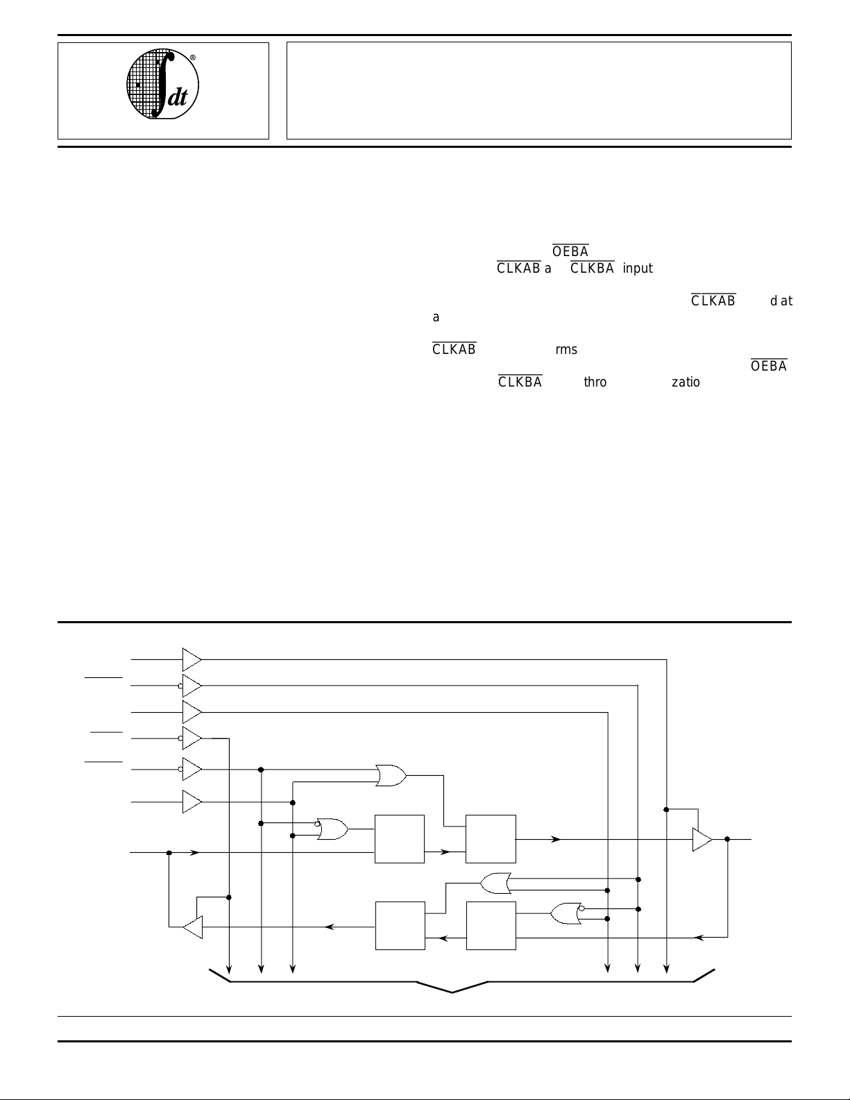
DESCRIPTION:
The FCT16500AT/CT/ET and FCT162500AT/CT/ET 18-
bit registered transceivers are built using advanced dual metal
CMOS technology. These high-speed, low-power 18-bit registered bus transceivers combine D-type latches and D-type
flip-flops to allow data flow in transparent, latched and clocked
modes. Data flow in each direction is controlled by outputenable (OEAB and
and clock (
CLKAB
OEBA
and
), latch enable (LEAB and LEBA)
CLKBA
) inputs. For A-to-B data flow,
the device operates in transparent mode when LEAB is HIGH.
When LEAB is LOW, the A data is latched if
CLKAB
is held at
a HIGH or LOW logic level. If LEAB is LOW, the A bus data is
stored in the latch/flip-flop on the HIGH-to-LOW transition of
CLKAB
port. Data flow from B port to A port is similar but uses
LEBA and
. OEAB performs the output enable function on the B
OEBA
CLKBA
. Flow-through organization of signal pins
simplifies layout. All inputs are designed with hysteresis for
improved noise margin.
The FCT16500AT/CT/ET are ideally suited for driving
high-capacitance loads and low-impedance backplanes. The
output buffers are designed with power off disable capability
to allow "live insertion" of boards when used as backplane
drivers.
The FCT162500AT/CT/ET have balanced output drive
with current limiting resistors. This offers low ground bounce,
minimal undershoot, and controlled output fall times–reducing
the need for external series terminating resistors. The
FCT162500AT/CT/ET are plug-in replacements for the
FCT16500AT/CT/ET and ABT16500 for on-board bus interface applications.
,
FUNCTIONAL BLOCK DIAGRAM
OEAB
CLKBA
LEBA
OEBA
CLKAB
LEAB
C
A1
The IDT logo is a registered trademark of Integrated Device Technology, Inc.
D
C
D
TO 17 OTHER CHANNELS
MILITARY AND COMMERCIAL TEMPERATURE RANGES AUGUST 1996
1996 Integrated Device Technology, Inc. 5.9 DSC-2548/7
C
B1
D
C
D
2548 drw 01
1
IDT54/74FCT16500AT/CT/ET, 162500AT/CT/ET
FAST CMOS 18-BIT REGISTERED TRANSCEIVER MILITARY AND COMMERCIAL TEMPERATURE RANGES
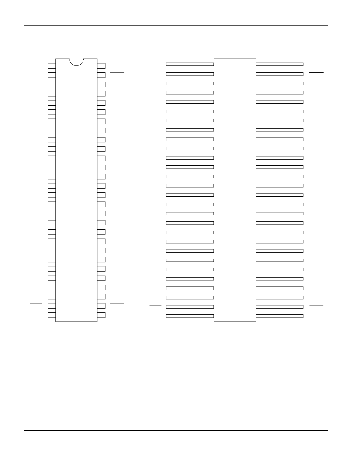
PIN CONFIGURATIONS
OEAB
LEAB
A
GND
A
A3
VCC
A4
A5
A
GND
A7
A8
A9
A
A11
A12
GND
A13
A14
A
VCC
A16
A
GND
A18
OEBA
LEBA
OEAB
LEAB
A
GND
A
A3
VCC
A4
A5
A
GND
A7
A8
A9
A
A11
A12
GND
A13
A14
A
VCC
A16
A
GND
A18
OEBA
LEBA
1
2
6
10
15
17
48
43
56
55
54
53
52
51
50
49
47
46
45
44
42
41
40
39
38
37
36
35
34
33
3225
31
30
29
GND
CLKAB
B1
GND
2
B
B3
VCC
4
B
B5
B6
GND
B7
B8
B9
B10
B11
B
12
GND
B13
B14
B15
VCC
16
B
B17
GND
18
B
CLKBA
GND
1
2
1
3
4
2
5
6
7
8
9
6
10
11
12
13
14
SO56-1
10
15
SO56-2
SO56-3
16
17
18
19
20
15
21
22
23
17
24
26
27
28
1
2
3
4
5
6
7
8
9
10
11
12
13
14
15
16
17
18
19
20
21
22
23
24
26
27
28
E56-1
56
55
54
53
52
51
50
49
48
47
46
45
44
43
42
41
40
39
38
37
36
35
34
33
3225
31
30
29
GND
CLKAB
B1
GND
B
2
B3
VCC
B
4
B5
B6
GND
B7
B8
B9
B10
B11
B
12
GND
B13
B14
B15
VCC
B
16
B17
GND
B
18
CLKBA
GND
SSOP/
TSSOP/TVSOP
TOP VIEW
2548 drw 02
CERPACK
2548 drw 03
TOP VIEW
5.9 2
IDT54/74FCT16500AT/CT/ET, 162500AT/CT/ET
FAST CMOS 18-BIT REGISTERED TRANSCEIVER MILITARY AND COMMERCIAL TEMPERATURE RANGES
PIN DESCRIPTION
Pin Names Description
OEAB A-to-B Output Enable Input
OEBA
LEAB A-to-B Latch Enable Input
LEBA B-to-A Latch Enable Input
CLKAB
CLKBA
Ax A-to-B Data Inputs or B-to-A 3-State Outputs
Bx B-to-A Data Inputs or A-to-B 3-State Outputs
B-to-A Output Enable Input (Active LOW)
A-to-B Clock Input (Active LOW)
B-to-A Clock Input (Active LOW)
2548 tbl 01
FUNCTION TABLE
(1,4)
Inputs Outputs
OEAB LEAB
CLKAB
CLKAB
Ax Bx
LXX XZ
HHX LL
HHX HH
HL↓ LL
HL↓ HH
HLH XB
HLL XB
NOTES: 2548 tbl 02
1. A-to-B data flow is shown. B-to-A data flow is similar but uses
LEBA, and
2. Output level before the indicated steady-state input conditions were
established.
3. Output level before the indicated steady-state input conditions were
established, provided that
4. H = HIGH Voltage Level
L = LOW Voltage Level
X = Don't Care
Z = High-impedance
↓ = HIGH-to-LOW Transition
CLKBA
.
CLKAB
was LOW before LEAB went LOW.
(2)
(3)
OEBA
,
ABSOLUTE MAXIMUM RATINGS
(1)
Symbol Description Max. Unit
Terminal Voltage with Respect to
(2)
V
TERM
V
TERM
T
STG
I
OUT
NOTES:
1. Stresses greater than those listed under ABSOLUTE MAXIMUM RATINGS may cause permanent damage to the device. This is a stress rating
only and functional operation of the device at these or any other conditions
above those indicated in the operational sections of this specification is
not implied. Exposure to absolute maximum rating conditions for
extended periods may affect reliability.
2. All device terminals except FCT162XXXT Output and I/O terminals.
3. Output and I/O terminals for FCT162XXXT.
GND
Terminal Voltage with Respect to
(3)
GND
Storage Temperature –65 to +150°C
DC Output Current –60 to +120 mA
–0.5 to +7.0 V
–0.5 to
V
CC
+0.5
2548 lnk 03
V
CAPACITANCE (TA = +25°C, f = 1.0MHz)
Symbol Parameter
CIN Input
Capacitance
CI/O I/O
Capacitance
NOTE:
1. This parameter is measured at characterization but not tested.
(1)
Conditions Typ. Max. Unit
VIN = 0V 3.5 6.0 pF
VOUT = 0V 3.5 8.0 pF
2548 lnk 04
5.9 3
 Loading...