

Integrated Device Technology Inc IDT74FCT164245TPVB, IDT74FCT164245TPV, IDT74FCT164245TPAB, IDT74FCT164245TPA, IDT74FCT164245TEB Datasheet
...
Integrated Device Technology, Inc.
FAST CMOS 16-BIT
BIDIRECTIONAL
3.3V TO 5V TRANSLATOR
IDT54/74FCT164245T
FEATURES:
• 0.5 MICRON CMOS Technology
• Bidirectional interface between 3.3V and 5V busses
• Control inputs can be driven from either 3.3V
or 5V circuits
• ESD >2000V per MIL-STD-883, Method 3015;
>200V using machine model (C = 200pF, R = 0)
• 25 MIL Center SSOP and Cerpack Packages
• Extended commercial range of -40°C to +85°C
•VCC1 = 5V ±10%, VCC2 = 2.7V to 3.6V
• High drive outputs (-32mA IOH, 64mA IOL) on 5V port
• Power-off disable on both ports permits "live insertion"
• Typical V
OLP (Output Ground Bounce) < 0.9V at
VCC1 = 5V, VCC2 = 3.3V, TA = 25°C
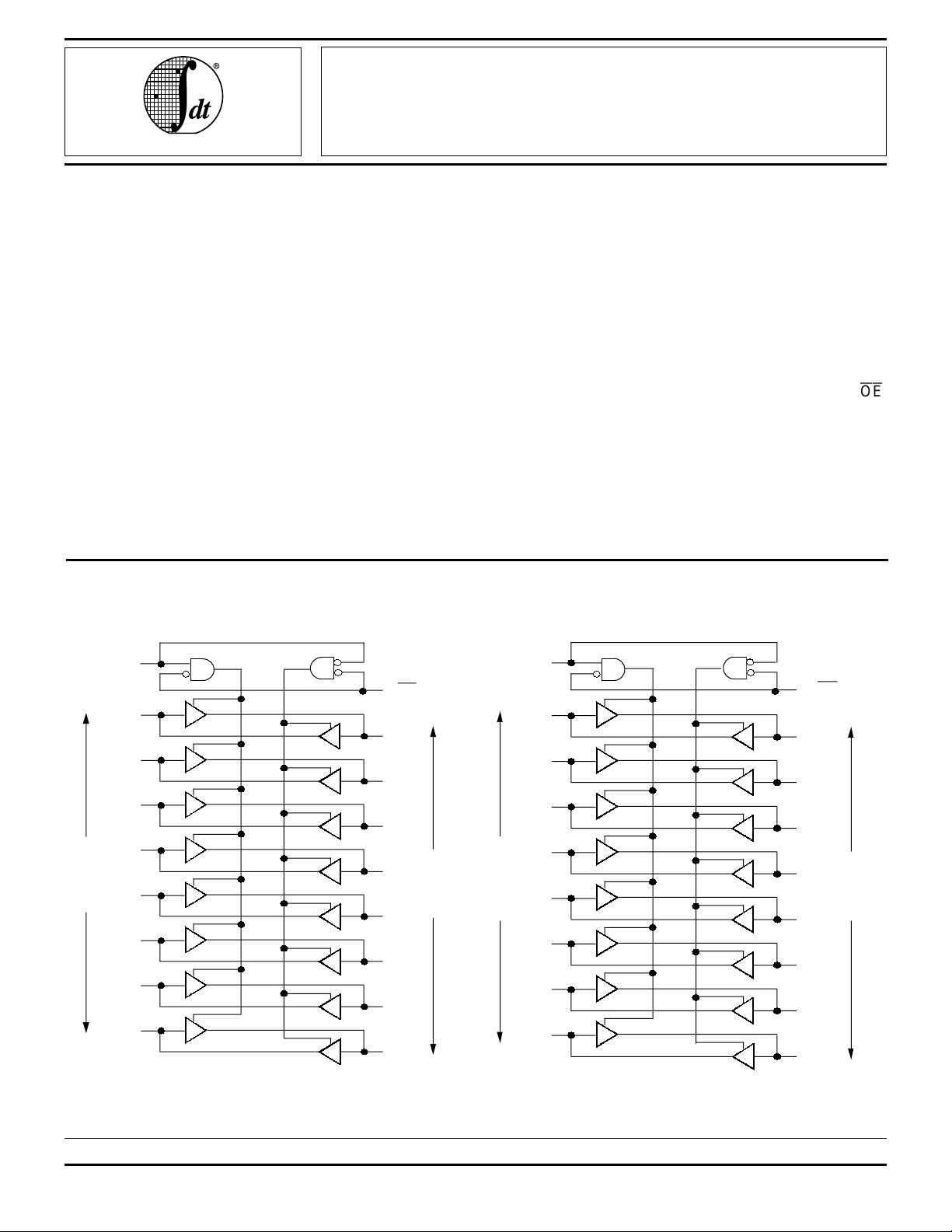
FUNCTIONAL BLOCK DIAGRAM
DESCRIPTION:
The FCT164245T 16-bit 3.3V-to-5V translator is built
using advanced dual metal CMOS technology. This highspeed, low-power transceiver is designed to interface between a 3.3V bus and a 5V bus in a mixed 3.3V/5V supply
environment. This enables system designers to interface TTL
compatible 3.3V components with 5V components. The
direction and output enable controls operate these devices as
either two independent 8-bit transceivers or one 16-bit transceiver. The A port interfaces with the 3.3V bus; the B port
interfaces with the 5V bus. The direction control (xDIR) pin
controls the direction of data flow. The output enable (xOE)
overrides the direction control and disables both ports. These
control signals can be driven from either 3.3V or 5V devices.
The FCT164245T is ideally suited for driving high capacitance loads and low impedance backplanes. The output
buffers are designed with Power-Off Disable capability to
allow "hot insertion" of boards when used as backplane
drivers. They also allow interface between a mixed supply
system and external 5V peripherals.
1
DIR
1A1
1
A
2
1
A
3
A
4
1
1
A
5
3.3V PORT
1
A
6
A
7
1
1
A
8
1
OE
B
1
1
B
1
B
1
B
B
1
1
B
B
1
B
1
2555 drw 01
1
2
3
4
5
6
7
8
5V PORT
2 DIR
2A1
2
A2
2
A3
2
A4
2
A5
3.3V PORT
2
A6
2
A7
2
A8
2OE
B1
2
2
B2
B3
2
2
B4
2
B5
B6
2
B7
2
B8
2
2555 drw 02
5V PORT
The IDT logo is a registered trademark of Integrated Device Technology, Inc.
MILITARY AND COMMERCIAL TEMPERATURE RANGES FEBRUARY 1996
1996 IIntegrated Device Technology, Inc. 8.16 DSC-2555/4
1
IDT54/74FCT164245T
FAST CMOS 16-BIT BIDIRECTIONAL 3.3V-TO-5V TRANSLATOR MILITARY AND COMMERCIAL TEMPERATURE RANGES
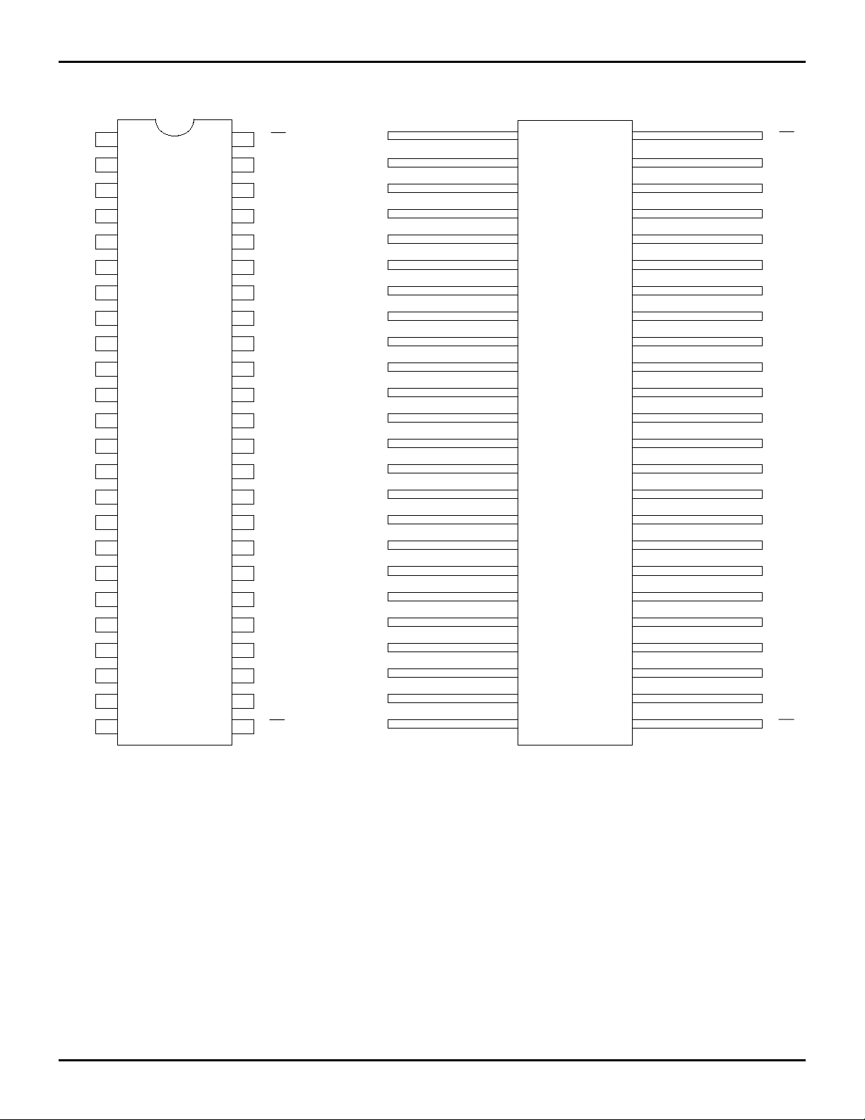
PIN CONFIGURATIONS
1
DIR
1B1
1B2
GND
1B3
B
1
V
CC1
B
1
B
1
GND
B
1
B
1
B
2
2B2
GND
B
2
B
2
1
2
3
4
5
4
6
7
5
6
8
9
10
7
8
11
12
SO48-1
48
47
46
45
44
43
42
41
40
39
38
37
1
OE
1A1
1
A
2
GND
1A3
A
4
1
V
CC2
A
5
1
A
6
1
GND
A
7
1
A
8
1
1DIR
1B1
1B2
GND
1B3
1
B4
VCC1
B5
1
B6
1
GND
1
B7
B8
1
1
2
3
4
5
6
7
8
9
10
11
12
E48-1
48
47
46
45
44
43
42
41
40
39
38
37
1OE
1A1
A2
1
GND
1A3
1
A4
VCC2
A5
1
A6
1
GND
1
A7
A8
1
SO48-2
1
13
14
15
3
4
16
17
36
35
34
33
32
A
1
2
2
A
2
GND
A
3
2
A
4
2
B1
2
2B2
GND
B3
2
2
B4
13
14
15
16
17
36
35
34
33
32
A1
2
A2
2
GND
A3
2
2
A4
CC1
V
B
2
2
B
GND
B
2
B
2
DIR
2
18
5
6
19
20
21
7
8
22
23
24
31
30
29
28
27
26
25
V
CC2
A
5
2
2
A
6
GND
A
7
2
A
8
2
2
OE
2555 drw 03
CC1
V
B5
2
B6
2
GND
B7
2
2
B8
DIR
2
SSOP
TSSOP
TOP VIEW
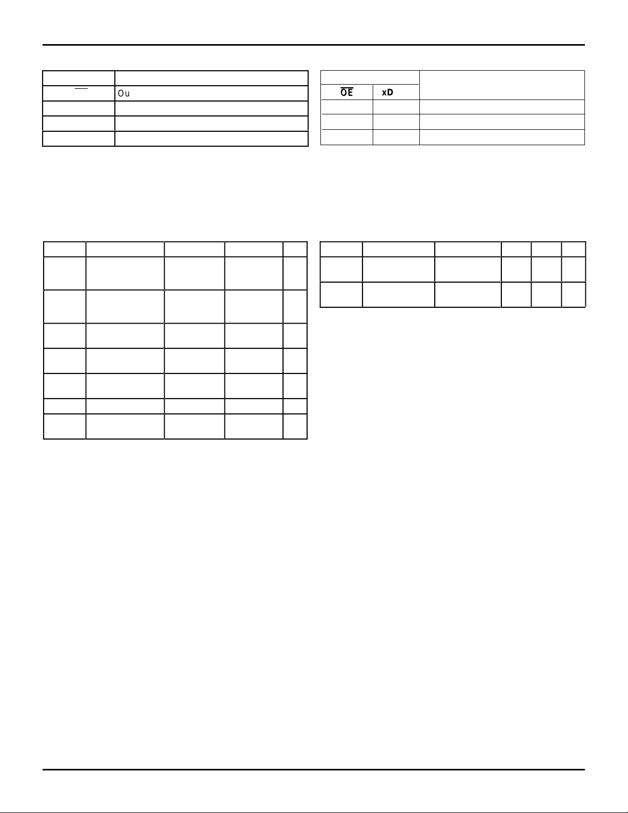
POWER SUPPLY SEQUENCING
In the IDT54/74FCT164245T the condition of VCC1 ≥
(VCC2 –0.5V) must be maintained at all times. For the range
of VCC1 = (VCC2 –0.5V) to VCC1 = (VCC2 +0.9V), both the A
and B ports will remain in a high impedance state.
18
19
20
21
22
23
24
CERPACK
TOP VIEW
31
30
29
28
27
26
25
2555 drw 04
VCC2
A5
2
A6
2
GND
A7
2
2
A8
2OE
8.16 2
IDT54/74FCT164245T
FAST CMOS 16-BIT BIDIRECTIONAL 3.3V-TO-5V TRANSLATOR MILITARY AND COMMERCIAL TEMPERATURE RANGES
PIN DESCRIPTION
Pin Names Description
x
OE
xDIR Direction Control Input
xAx Side A Inputs or 3-State Outputs (3.3V Port)
xBx Side B Inputs or 3-State Outputs (5V Port)
ABSOLUTE MAXIMUM RATINGS
Symbol Rating Commercial Military Unit
(2)
VTERM
(3)
VTERM
TA Operating
TBIAS Temperature
TSTG Storage
PT Power Dissipation 1.0 1.0 W
IOUT DC Output
NOTES:
1. Stresses greater than those listed under ABSOLUTE MAXIMUM RATINGS may cause permanent damage to the device. This is a stress rating
only and functional operation of the device at these or any other conditions
above those indicated in the operational sections of this specification is
not implied. Exposure to absolute maximum rating conditions for extended periods may affect reliability.
2. All device terminals except V
3. Power supply terminals VCC2.
Output Enable Input (Active LOW)
Terminal Voltage
–0.5 to +7.0 –0.5 to +7.0 V
with Respect to
GND
Terminal Voltage
with Respect to
GND
–0.5 to V
+0.5
–40 to +85 –55 to +125 °C
Temperature
–55 to +125 –65 to +135 °C
Under Bias
–55 to +125 –65 to +150 °C
Temperature
–60 to +120 –60 to +120 mA
Current
CC2.
CC1
(1)
–0.5 to V
+0.5
2555 tbl 01
CC1
2555 lnk 02
V
FUNCTION TABLE
(1)
Inputs
x
OE
OE
xDIR Outputs
L L Bus B Data to Bus A
L H Bus A Data to Bus B
H X High Z State
NOTE:
1. H = HIGH Voltage Level
L = LOW Voltage Level
X = Don't Care
Z = High Impedance
CAPACITANCE
Symbol Parameter
CIN Input
(TA = +25°C, f = 1.0MHz)
(1)
Conditions Typ. Max. Unit
VIN = 0V 3.5 6.0 pF
Capacitance
CI/O I/O
VOUT = 0V 3.5 8.0 pF
Capacitance
NOTE:
1. This parameter is measured at characterization but not tested.
2555 tbl 03
2555 lnk 04
8.16 3
 Loading...