

Integrated Device Technology Inc IDT74FCT163952CPVB, IDT74FCT163952CPV, IDT74FCT163952CPF, IDT74FCT163952CPAB, IDT74FCT163952CPA Datasheet
...
Integrated Device Technology, Inc.
The IDT Logo is a registered trademark of Integrated Device Technology, Inc.
3.3V CMOS
16-BIT REGISTERED
TRANSCEIVER
COMMERCIAL TEMPERATURE RANGE AUGUST 1996
1996 Integrated Device Technology, Inc. 8.10 DSC-3096/4
1
IDT74FCT163952A/B/C
FEATURES:
• 0.5 MICRON CMOS Technology
• Typical tSK(o) (Output Skew) < 250ps
• ESD > 2000V per MIL-STD-883, Method 3015;
> 200V using machine model (C = 200pF, R = 0)
• Packages include 25 mil pitch SSOP, 19.6 mil pitch
TSSOP and 15.7 mil pitch TVSOP
• Extended commercial range of -40°C to +85°C
•VCC = 3.3V ±0.3V, Normal Range or
VCC = 2.7 to 3.6V, Extended Range
• CMOS power levels (0.4µW typ. static)
• Rail-to-Rail output swing for increased noise margin
• Low Ground Bounce (0.3V typ.)
• Inputs (except I/O) can be driven by 3.3V or 5V
components
1OEAB
1CEBA
1CLKBA
1OEBA
1CEAB
1CLKAB
1A1
3096 drw 01
1B1
TO 7 OTHER CHANNELS
D
C
D
C
CE
CE
2OEAB
2CEBA
2CLKBA
2OEBA
2CEAB
2CLKAB
2A1
3096 drw 02
2B1
TO 7 OTHER CHANNELS
D
C
D
C
CE
CE
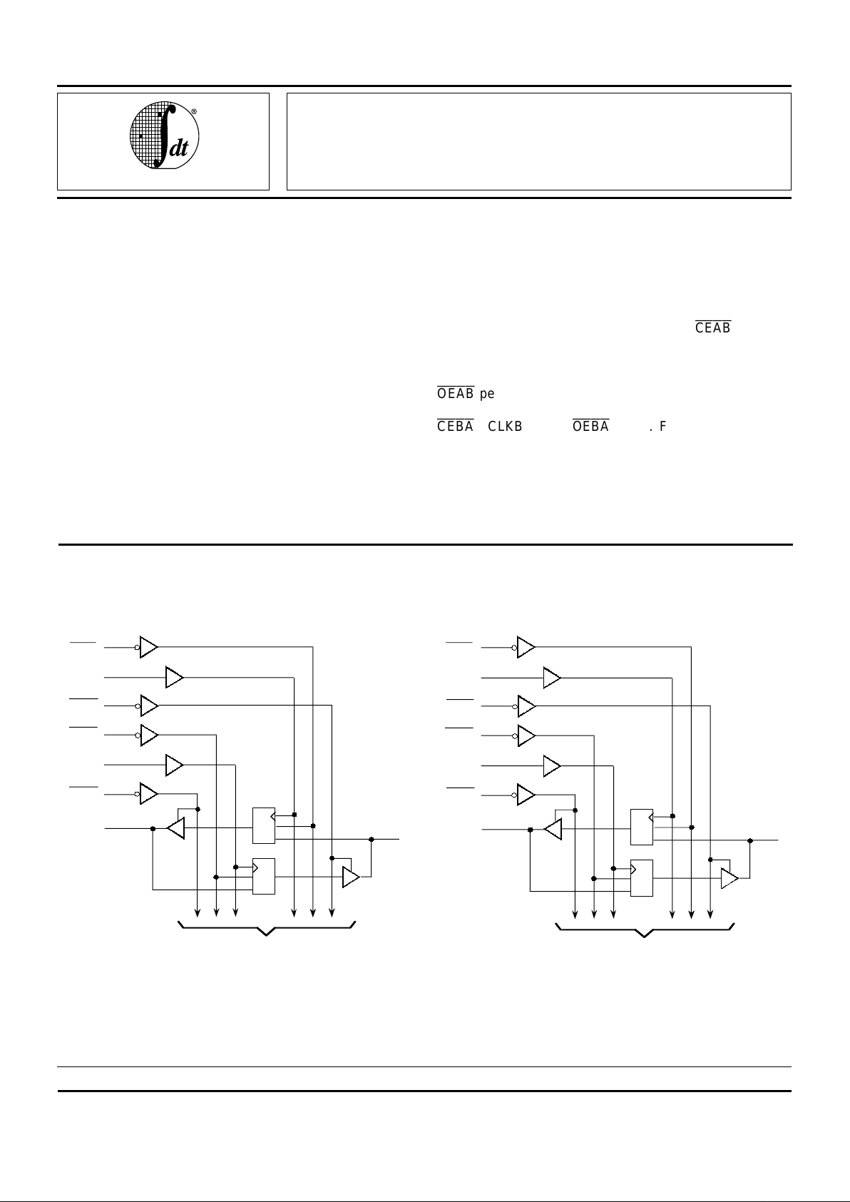
DESCRIPTION:
The FCT163952A/B/C 16-bit registered transceivers are
built using advanced dual metal CMOS technology. These
high-speed, low-power devices are organized as two independent 8-bit D-type registered transceivers with separate input
and output control for independent control of data flow in either
direction. For example, the A-to-B Enable (x
CEAB
) must be
LOW to enter data from the A port. xCLKAB controls the
clocking function. When xCLKAB toggles from LOW-to-HIGH,
the data present on the A port will be clocked into the register.
x
OEAB
performs the output enable function on the B port.
Data flow from the B port to A port is similar but requires using
x
CEBA
, xCLKBA, and x
OEBA
inputs. Full 16-bit operation is
achieved by tying the control pins of the independent transceivers together.
The FCT163952A/B/C have series current limiting resistors. These offer low ground bounce, minimal undershoot, and
controlled output fall times–reducing the need for external
series terminating resistors.
FUNCTIONAL BLOCK DIAGRAM
8.10 2
IDT74FCT163952/A/C
3.3V CMOS 16-BIT REGISTERED TRANSCEIVER COMMERCIAL TEMPERATURE RANGE
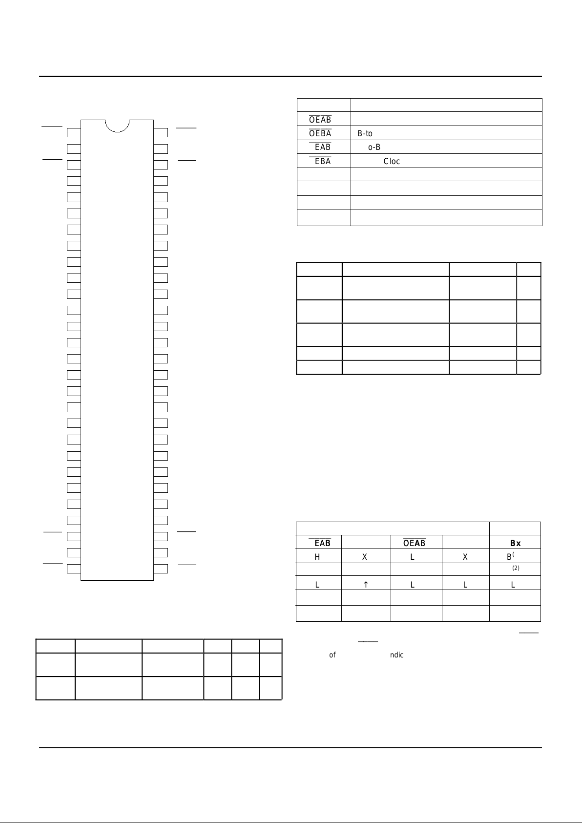
PIN CONFIGURATIONS
3096 drw 03
1B1
1
B
2
GND
1B3
1
B
4
V
CC
1
B
5
1
B
6
1
OEBA
1B7
1
B
8
2
B
1
2
B
2
GND
2B3
2
B
4
V
CC
2
B
5
GND
1
CLKBA
2B7
2
B
6
2
B
8
GND
2
CLKBA
2
OEBA
1
CLKAB
GND
1A1
1
A
2
V
CC
1
A
3
1
A
4
GND
1A5
1
A
6
1
A
7
1
A
8
GND
2A1
2
A
2
V
CC
2
A
3
2
A
5
2
A
4
2
A
7
GND
2A8
2
CLKAB
2A6
1
OEAB
1
CEAB
2
OEAB
2
CEAB
2
CEBA
1
CEBA
47
37
38
39
40
41
42
43
44
45
46
33
34
35
36
56
55
49
50
51
52
53
54
48
1
2
3
4
5
6
7
8
9
10
12
13
14
15
16
17
18
19
20
11
21
22
23
24
SSOP/
TSSOP/TVSOP
TOP VIEW
SO56-1
SO56-2
SO56-3
29
30
31
3225
26
27
28
PIN DESCRIPTION
Pin Names Description
x
OEAB
A-to-B Output Enable Input (Active LOW)
x
OEBA
B-to-A Output Enable Input (Active LOW)
x
CEAB
A-to-B Clock Enable Input (Active LOW)
x
CEBA
B-to-A Clock Enable Input (Active LOW)
xCLKAB A-to-B Clock Input
xCLKBA B-to-A Clock Input
xAx A-to-B Data Inputs or B-to-A 3-State Outputs
xBx B-to-A Data Inputs or A-to-B 3-State Outputs
3096 tbl 01
ABSOLUTE MAXIMUM RATINGS
(1)
Symbol Description Max. Unit
VTERM
(2)
Terminal Voltage with
Respect to GND
–0.5 to +4.6 V
VTERM
(3)
Terminal Voltage with
Respect to GND
–0.5 to +7.0 V
VTERM
(4)
Terminal Voltage with
Respect to GND
–0.5 to
V
CC + 0.5
V
TSTG Storage Temperature –65 to +150 °C
IOUT DC Output Current –60 to +60 mA
3096 lnk 03
NOTES:
1. Stresses greater than those listed under ABSOLUTE MAXIMUM RATINGS may cause permanent damage to the device. This is a stress rating
only and functional operation of the device at these or any other conditions
above those indicated in the operational sections of this specification is
not implied. Exposure to absolute maximum rating conditions for extended periods may affect reliability.
2. Vcc terminals.
3. Input terminals.
4. Output and I/O terminals.
FUNCTION TABLE
(1,3)
Inputs Outputs
x
CEAB
CEAB
xCLKAB x
OEAB
OEAB
xAx xBx
HXL XB
(2)
XLL XB
(2)
L ↑ LLL
L↑LHH
XXH XZ
NOTES: 3096 tbl 02
1. A-to-B data flow is shown: B-to-A data flow is similar but uses, x
CEBA
,
xCLKBA, and x
OEBA
.
2. Level of B before the indicated steady-state input conditions were
established.
3. H = HIGH Voltage Level
L = LOW Voltage Level
X = Don't Care
↑ = LOW-to-HIGH Transition
Z = High-impedance
CAPACITANCE (TA = +25°C, f = 1.0MHz)
NOTE:
1. This parameter is measured at characterization but not tested.
Symbol Parameter
(1)
Conditions Typ. Max. Unit
CIN Input
Capacitance
VIN = 0V 3.5 6.0 pF
CI/O I/O
Capacitance
VOUT = 0V 3.5 8.0 pF
3096 lnk 04
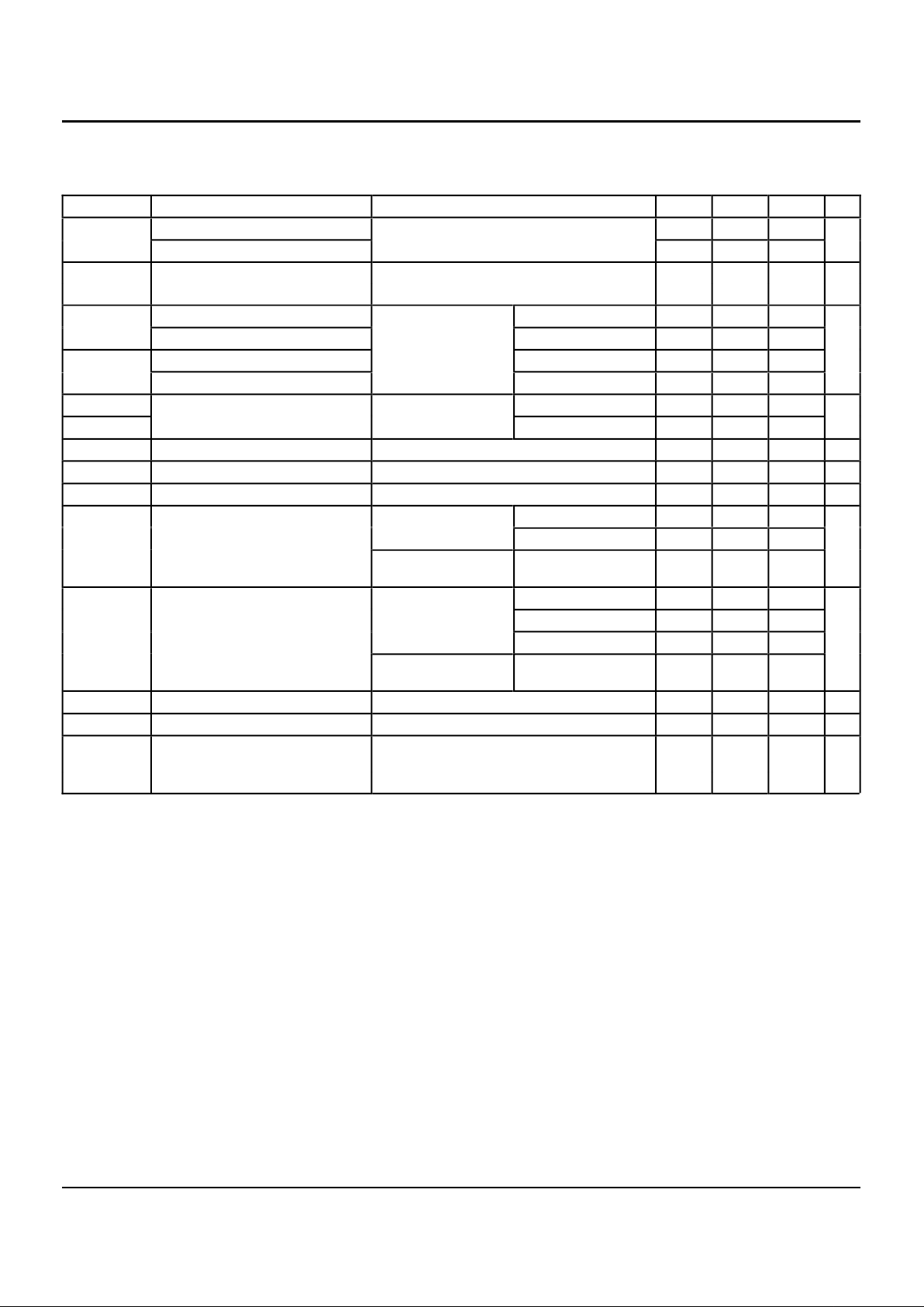
8.10 3
IDT74FCT163952/A/C
3.3V CMOS 16-BIT REGISTERED TRANSCEIVER COMMERCIAL TEMPERATURE RANGE
DC ELECTRICAL CHARACTERISTICS OVER OPERATING RANGE
Following Conditions Apply Unless Otherwise Specified:
Commercial: TA = –40°C to +85°C, VCC = 2.7V to 3.6V
Symbol Parameter Test Conditions
(1)
Min. Typ.
(2)
Max. Unit
V
IH
Input HIGH Level (Input pins) Guaranteed Logic HIGH Level 2.0 — 5.5 V
Input HIGH Level (I/O pins) 2.0 — VCC+0.5
V
IL
Input LOW Level Guaranteed Logic LOW Level –0.5
—
0.8 V
(Input and I/O pins)
I
I H
Input HIGH Current (Input pins) VCC = Max. VI = 5.5V —
—
±
1
µ
A
Input HIGH Current (I/O pins) VI = V
CC
—
—
±
1
I
I L
Input LOW Current (Input pins) VI = GND —
—
±
1
Input LOW Current (I/O pins) VI = GND —
—
±
1
I
OZH
High Impedance Output Current VCC = Max. VO = V
CC
—
—
±
1
µ
A
I
OZL
(3-State Output pins) VO = GND —
—
±
1
V
IK
Clamp Diode Voltage VCC = Min., I
IN
= –18mA —
–
0.7
–
1.2 V
I
ODH
Output HIGH Current VCC = 3.3V, V
IN
= V
IH
or V
IL, VO
= 1.5V
(3)
–36 –60 –110 mA
I
ODL
Output LOW Current VCC = 3.3V, V
IN
= V
IH
or V
IL, VO
= 1.5V
(3)
50 90 200 mA
V
OH
Output HIGH Voltage VCC = Min. IOH = –0.1mA V
CC
–
0.2 — — V
VIN = V
IH
or V
IL
IOH = –3mA 2.4 3.0 —
VCC = 3.0V
V
IN
= V
IH
or V
IL
IOH = –8mA 2.4
(5)
3.0 —
V
OL
Output LOW Voltage VCC = Min. IOL = 0.1mA — — 0.2 V
VIN = V
IH
or V
IL
IOL = 16mA — 0.2 0.4
IOL = 24mA — 0.3 0.55
VCC = 3.0V
V
IN
= V
IH
or V
IL
IOL = 24mA — 0.3 0.50
I
OS
Short Circuit Current
(4)
VCC = Max., VO = GND
(3)
–60
–
135 –240 mA
V
H
Input Hysteresis
—
— 150
—
mV
I
CCL
I
CCH
Quiescent Power Supply Current VCC = Max.,
V
IN
= GND or V
CC
— 0.1 10
µ
A
I
CCZ
3096 lnk 05
NOTES:
1. For conditions shown as Max. or Min., use appropriate value specified under Electrical Characteristics for the applicable device type.
2. Typical values are at Vcc = 3.3V, +25°C ambient.
3. Not more than one output should be tested at one time. Duration of the test should not exceed one second.
4. This parameter is guaranteed but not tested.
5. V
OH = VCC –0.6V at rated current.
 Loading...