


IDT IDT74CVTLV3384 User Manual
查询IDT74CBTLV3384供应商
IDT74CBTLV3384
LOW-VOLTAGE 10-BIT BUS SWITCH
INDUSTRIAL TEMPERATURE RANGE
LOW-VOLTAGE 10-BIT
BUS SWITCH
FEA TURES:
ΩΩ
•5
Ω A/B bi-directional bus switch
ΩΩ
• Isolation under power-off conditions
• Over-voltage tolerant
• Latch-up performance exceeds 100mA
•VCC = 2.3V - 3.6V, Normal Range
• ESD > 2000V per MIL-STD-883, Method 3015;
> 200V using machine model (C = 200pF, R = 0)
• Available in SSOP, QSOP and TSSOP packages
APPLICA TIONS:
• 3.3V High Speed Bus Switching and Bus Isolation
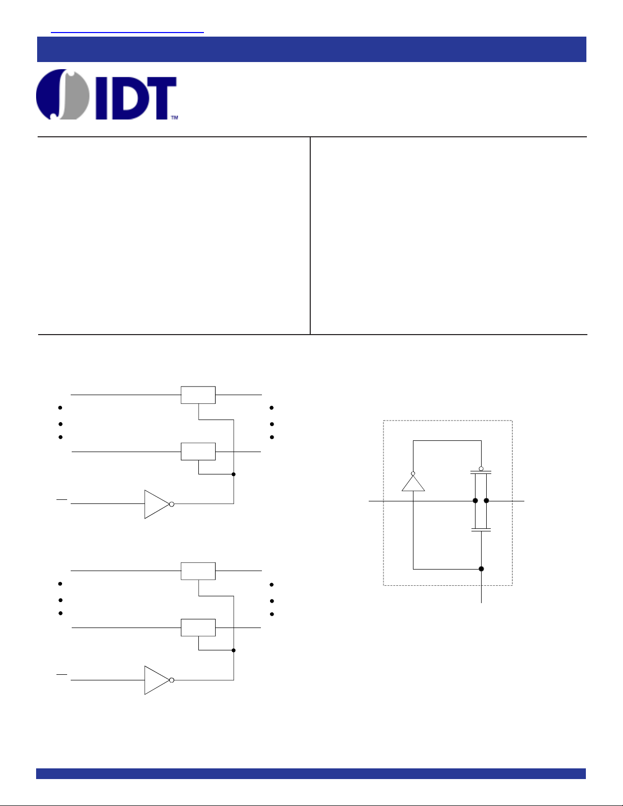
FUNCTIONAL BLOCK DIAGRAM
IDT74CBTLV3384
DESCRIPTION:
The CBTLV3384 is a ten bit high-speed bus switch with low on-state
resistance of the switch allowing connections to be made with minimal
propagation delay.
The device is organized as dual 5-bit bus switches with separate outputenable (OE) inputs, to allow use as two 5-bit bus switches or one 10-bit bus
switch. When OE is low, the associated 5-bit bus switch is on and A port is
connected to B port. When OE is high, the switch is open, and a highimpedance state exists between the two ports.
To ensure the high-impedance state during power up or power down,
OE should be tied to V
the resistor is determined by the current-sinking capability of the driver.
SIMPLIFIED SCHEMATIC, EACH SWITCH
CC through a pullup resistor; the minimum value of
1A1
1A5
1OE
2A1
2A5
2OE
3
11
1
14
22
13
SW
SW
SW
SW
2
1B1
10
1B5
A
15
2B1
OE
10
2B5
B
The IDT logo is a registered trademark of Integrated Device Technology, Inc.
SEPTEMBER 2001INDUSTRIAL TEMPERATURE RANGE
1
© 2001 Integrated Device Technology, Inc. DSC-5742/4
IDT74CBTLV3384
LOW-VOLTAGE 10-BIT BUS SWITCH
INDUSTRIAL TEMPERATURE RANGE
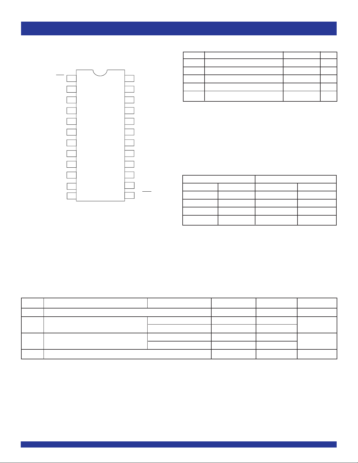
PIN CONFIGURATION
1OE
1B1
1A1
1A2
1B2
1B3
1A3
1A4
1B4
1B5
1A
GND
5
1
2
3
4
5
6
7
8
9
10
11
12
SSOP/ QSOP/ TSSOP
TOP VIEW
24
23
22
21
20
19
18
17
16
15
14
13
VCC
2B
2A5
2A4
2B4
2B3
2A3
2A2
2B2
2B1
2A1
2OE
ABSOLUTE MAXIMUM RATINGS
Symbol Description Max Unit
VCC SupplyVoltage Range –0.5 to +4.6 V
VI Input Voltage Range –0.5 to +4.6 V
Continuous Channel Current 128 mA
5
IIK Input Clamp Current, VI/O < 0 –50 mA
T
STG Storage Temperature –65 to +150 °C
NOTE:
1. Stresses greater than those listed under ABSOLUTE MAXIMUM RATINGS may cause
permanent damage to the device. This is a stress rating only and functional operation
of the device at these or any other conditions above those indicated in the operational
sections of this specification is not implied. Exposure to absolute maximum rating
conditions for extended periods may affect reliability.
FUNCTION TABLE
Input Inputs/Outputs
1OE 2OE 1B1 - 1B52B1 - 2B5
LL1A1 - 1A52A1 - 2A5
LH1A1 - 1A5 Z
HL Z2A1 - 2A5
HH Z Z
NOTE:
1. H = HIGH Voltage Level
L = LOW Voltage Level
Z = High Impedance
(1)
(1)
OPERATING CHARACTERISTICS, TA = 25°C
Symbol Parameter Test Conditions Min. Max. Unit
VCC Supply Voltage 2.3 3.6 V
V
IH High-Level Control Input Voltage VCC = 2.3V to 2.7V 1.7 — V
VCC = 2.7V to 3.6V 2 —
VIL Low-Level Control Input Voltage VCC = 2.3V to 2.7V — 0.7 V
VCC = 2.7V to 3.6V — 0.8
A Operating Free-Air Temperature −40 85 ° C
T
NOTE:
1. All unused control inputs of the device must be held at VCC or GND to ensure proper device operation.
(1)
2