

查询IDT72V81供应商
3.3 Volt CMOS DUAL ASYNCHRONOUS FIFO
DUAL 512 x 9, DUAL 1,024 x 9
DUAL 2,048 x 9, DUAL 4,096 X 9
DUAL 8,192 X 9
FEATURES:
♦♦
The IDT72V81 is equivalent to two IDT72V01 - 512 x 9 FIFOs
♦
♦♦
♦♦
The IDT72V82 is equivalent to two IDT72V02 - 1,024 x 9 FIFOs
♦
♦♦
♦♦
The IDT72V83 is equivalent to two IDT72V03 - 2,048 x 9 FIFOs
♦
♦♦
♦♦
The IDT72V84 is equivalent to two IDT72V04 - 4,096 x 9 FIFOs
♦
♦♦
♦♦
The IDT72V85 is equivalent to two IDT72V05 - 8,192 x 9 FIFOs
♦
♦♦
♦♦
Low power consumption
♦
♦♦
— Active: 330 mW (max.)
— Power-down: 18 mW (max.)
♦♦
Ultra high speed—15 ns access time
♦
♦♦
♦♦
Asynchronous and simultaneous read and write
♦
♦♦
♦♦
Offers optimal combination of data capacity, small foot print
♦
♦♦
and functional flexibility
♦♦
Ideal for bidirectional, width expansion, depth expansion, bus-
♦
♦♦
matching, and data sorting applications
♦♦
Status Flags: Empty, Half-Full, Full
♦
♦♦
♦♦
Auto-retransmit capability
♦
♦♦
♦♦
High-performance CEMOS™ technology
♦
♦♦
♦♦
Space-saving TSSOP package
♦
♦♦
♦♦
Industrial temperature range (–40
♦
♦♦
°°
°C to +85
°°
°°
°C) is available
°°
IDT72V81
IDT72V82
IDT72V83
IDT72V84
IDT72V85
DESCRIPTION:
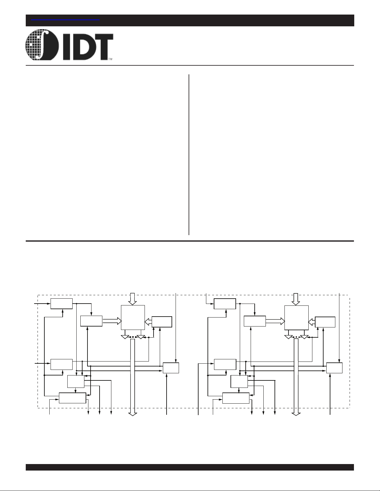
The IDT72V81/72V82/72V83/72V84/72V85 are dual-FIFO memories that
load and empty data on a first-in/first-out basis. These devices are functional and
compatible to two IDT72V01/72V02/72V03/72V04/72V05 FIFOs in a single
package with all associated control, data, and flag lines assigned to separate
pins. The devices use Full and Empty flags to prevent data overflow and
underflow and expansion logic to allow for unlimited expansion capability in both
word size and depth.
The reads and writes are internally sequential through the use of ring
pointers, with no address information required to load and unload data. Data
is toggled in and out of the devices through the use of the Write (W) and Read
(R) pins.
The devices utilize a 9-bit wide data array to allow for control and parity
bits at the user’s option. This feature is especially useful in data communications
applications where it is necessary to use a parity bit for transmission/reception
error checking. It also features a Retransmit (RT) capability that allows for reset
of the read pointer to its initial position when RT is pulsed low to allow for
retransmission from the beginning of data. A Half-Full Flag is available in the
single device mode and width expansion modes.
These FIFOs are fabricated using IDT’s high-speed CMOS technology.
They are designed for those applications requiring asynchronous and simultaneous read/writes in multiprocessing and rate buffer applications.
FUNCTIONAL BLOCK DIAGRAM
DATA INPUTS
(DA0-DA8)
WA
RA
WRITE
CONTROL
READ
CONTROL
XIA
FLAG
LOGIC
EXPANSION
LOGIC
XOA/HFA
WRITE
POINTER
THREE-
STATE
BUFFERS
FFA EFA
RAM
ARRAY A
512 x 9
1,024 x 9
2,048 x 9
4,096 x 9
8,192 x 9
DATA
OUTPUTS
0
-QA8)
(QA
POINTER
READ
FLA/RTA
RSA
RESET
LOGIC
RB
WB
WRITE
CONTROL
READ
CONTROL
XIB
FLAG
LOGIC
EXPANSION
LOGIC
XOB/HFB
WRITE
POINTER
THREE-
STATE
BUFFERS
FFB EFB
DATA INPUTS
(DB
0
-DB8)
RAM
ARRAY A
512 x 9
1,024 x 9
2,048 x 9
4,096 x 9
8,192 x 9
DATA
OUTPUTS
0
-QB8)
(QB
READ
POINTER
RESET
LOGIC
FLB/RTB
RSB
3966 drw 01
August 1999
1999 Integrated Device Technology, Inc. DSC-3966/-
1
Commercial Temperature RangeIDT72V81/72V82/72V83/72V84/72V85
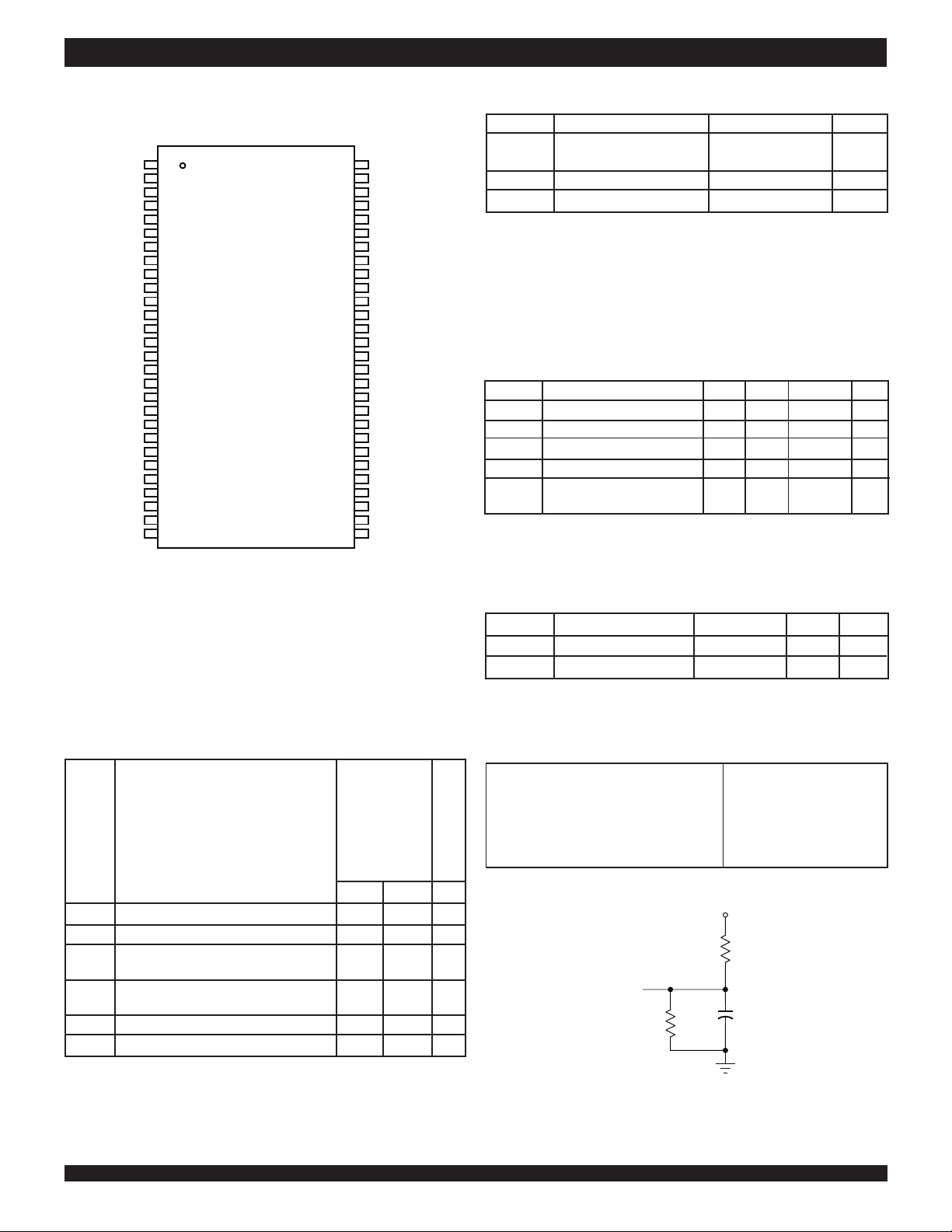
PIN CONFIGURATION ABSOLUTE MAXIMUM RATINGS
Symbol Rating Commercial Unit
V
TERM Terminal Voltage –0.5 to +7.0 V
FFA
QA
QA
QA
QA
QA
GND
RA
QA
QA
QA
QA
XOA/HFA
EFA
FFB
QB
QB
QB
QB
QB
GND
RB
QB
QB
QB
QB
XOB/HFB
EFB
1
0
2
1
3
2
4
3
5
8
6
7
8
4
9
5
10
6
11
7
12
13
14
15
0
16
1
17
2
18
3
19
8
20
21
22
4
23
5
24
6
25
7
26
27
28
56
55
54
53
52
51
50
49
48
47
46
45
44
43
42
41
40
39
38
37
36
35
34
33
32
31
30
29
XIA
0
DA
DA
1
DA
2
DA
3
DA
8
WA
V
CC
DA
4
DA
5
DA
6
DA
7
FLA/RTA
RSA
XIB
0
DB
DB
1
DB
2
DB
3
DB
8
WB
CC
V
DB
4
DB
5
DB
6
DB
7
FLB/RTB
RSB
3966 drw 02
STG Storage Temperature –55 to +125 °C
T
OUT DC Output Current –50 to +50 mA
I
NOTE:
1. Stresses greater than those listed under ABSOLUTE MAXIMUM RATINGS may cause
permanent damage to the device. This is a stress rating only and functional operation of
the device at these or any other conditions above those indicated in the operational
sections of this specification is not implied. Exposure to absolute maximum rating
conditions for extended periods may affect reliability.
RECOMMENDED DC OPERATING
CONDITIONS
Symbol Parameter Min. Typ. Max. Unit
CC Supply Voltage 3.0 3.3 3.6 V
V
GND Supply Voltage 0 0 0 V
(1)
IH
V
(2)
IL
V
A Operating Temperature 0 — 70 °C
T
NOTES:
1. For RT/RS/XI input, V
2. 1.5V undershoots are allowed for 10ns once per cycle.
with Respect to GND
Input High Voltage 2.0 — VCC+0.5 V
Input Low Voltage — — 0.8 V
Commercial
IH = 2.6V (commercial).
TSSOP (SO56-2, order code: PA)
TOP VIEW
DC ELECTRICAL
CHARACTERISTICS
(Commercial: VCC = 3.3V±0.3V, TA = 0°C to +70°C)
Symbol Parameter Min. Max. Unit
(1)
LI
I
I
V
V
I
I
NOTES:
1. Measurements with 0.4 ≤ V
2. R ≥ V
3. Tested with outputs open (I
4. Tested at f = 20 MHz.
5. All Inputs = V
Input Leakage Current (Any Input) –1 1 µA
(2)
LO
Output Leakage Current –1 0 10 µA
OH Output Logic “1” Voltage 2.4 — V
OH = –2mA
I
OL Output Logic “0” Voltage — 0.4 V
OL = 8mA
I
(3,4)
CC1
Active Power Supply Current (both FIFOs) — 100 mA
(3,5)
CC2
Standby Current (R=W=RS=FL/RT=VIH)— 5mA
IH, 0.4 ≤ VOUT ≤ VCC.
CC - 0.2V or GND + 0.2V.
IN ≤ VCC.
OUT = 0).
(1)
IDT72V81
IDT72V82
IDT72V83
IDT72V84
IDT72V85
Commercial
A = 15, 20 ns
t
CAPACITANCE (TA = +25°C, f = 1.0 MHz)
Symbol Parameter
IN Input Capacitance VIN = 0V 8 pF
C
OUT Output Capacitance VOUT = 0V 8 pF
C
NOTE:
1. Characterized values, not currently tested.
(1)
Condition Max. Unit
AC TEST CONDITIONS
Input Pulse Levels GND to 3.0V
Input Rise/Fall Times 5ns
Input Timing Reference Levels 1.5V
Output Reference Levels 1.5V
Output Load See Figure 1
3.3V
330Ω
TO
OUTPUT
PIN
510Ω
or equivalent circuit
Figure 1. Output Load
*Includes scope and jib capacitances.
30pF*
3966 drw 03
2

IDT72V81/72V82/72V83/72V84/72V85
Commercial Temperature Range
AC ELECTRICAL CHARACTERISTICS
(1)
(Commercial: VCC = 3.3V±0.3V, TA = 0°C to +70°C)
Commercial
IDT72V81L15 IDT72V81L20
IDT72V82L15 IDT72V82L20
IDT72V83L15 IDT72V83L20
IDT72V84L15 IDT72V84L20
IDT72V85L15 IDT72V85L20
Symbol Parameter Min. Max. Min. Max. Unit
S Shift Frequency — 40 — 33.3 MHz
t
RC Read Cycle Time 25 — 30 — ns
t
A Access Time — 15 — 20 ns
t
RR Read Recovery Time 10 — 10 — ns
t
RPW Read Pulse Width
t
RLZ Read Pulse Low to Data Bus at Low Z
t
WLZ Write Pulse High to Data Bus at Low Z
t
DV Data Valid from Read Pulse High 5 — 5 — ns
t
RHZ Read Pulse High to Data Bus at High Z
t
t
WC Write Cycle Time 25 — 30 — ns
WPW Write Pulse Width
t
WR Write Recovery Time 10 — 10 — ns
t
DS Data Set-up Time 11 — 12 — ns
t
DH Data Hold Time 0 — 0 — ns
t
RSC Reset Cycle Time 25 — 30 — ns
t
RS Reset Pulse Width
t
RSS Reset Set-up Time
t
t
RSR Reset Recovery Time 10 — 10 — ns
RTC Retransmit Cycle Time 25 — 30 — ns
t
RT Retransmit Pulse Width
t
RTS Retransmit Set-up Time
t
RTR Retransmit Recovery Time 10 — 10 — ns
t
EFL Reset to Empty Flag Low — 25 — 30 ns
t
HFH,FFH Reset to Half-Full and Full Flag High — 25 — 30 ns
t
RTF Retransmit Low to Flags Valid — 25 — 30 ns
t
t
REF Read Low to Empty Flag Low — 15 — 20 ns
RFF Read High to Full Flag High — 15 — 20 ns
t
RPE Read Pulse Width after EF High 15 — 20 — ns
t
WEF Write High to Empty Flag High — 15 — 20 ns
t
WFF Write Low to Full Flag Low — 15 — 20 ns
t
WHF Write Low to Half-Full Flag Low — 25 — 30 ns
t
RHF Read High to Half-Full Flag High — 25 — 30 ns
t
WPF Write Pulse Width after FF High 15 — 20 — ns
t
t
XOL Read/Write to XO Low — 15 — 20 ns
XOH Read/Write to XO High — 15 — 2 0 ns
t
XI XI Pulse Width
t
XIR XI Recovery Time 10 — 10 — ns
t
XIS XI Set-up Time 10 — 1 0 — ns
t
NOTES:
1. Timings referenced as in AC Test Conditions.
2. Pulse widths less than minimum value are not allowed.
3. Values guaranteed by design, not currently tested.
4. Only applies to read data flow-through mode.
(2)
(3)
(3, 4)
(3)
(2)
(2)
(3)
(2)
(3)
(2)
15 — 20 — ns
3—3—ns
5—5—ns
—15—15ns
15 — 20 — ns
15 — 20 — ns
15 — 20 — ns
15 — 20 — ns
15 — 20 — ns
15 — 20 — ns
3

Commercial Temperature RangeIDT72V81/72V82/72V83/72V84/72V85
SIGNAL DESCRIPTIONS
INPUTS:
DATA IN (D0 – D8)
Data inputs for 9-bit wide data.
CONTROLS:
RESET (
During reset, both internal read and write pointers are set to the first location.
A reset is required after power up before a write operation can take place. Both
the Read Enable (
state during the window shown in Figure 2, (i.e., tRSS before the rising
edge of
RSRS
RS. Half-Full Flag (
RSRS
WRITE ENABLE (
is not set. Data set-up and hold times must be adhered to with respect to the rising
edge of the Write Enable (W). Data is stored in the RAM array sequentially and
independently of any on-going read operation.
operation, the Half-Full Flag (HF) will be set to low and will remain set until the
difference between the write pointer and read pointer is less than or equal to
one half of the total memory of the device. The Half-Full Flag (HF) is then reset
by the rising edge of the read operation.
operations. Upon the completion of a valid read operation, the Full Flag (FF)
will go high after tRFF, allowing a valid write to begin. When the FIFO is full, the
internal write pointer is blocked from W, so external changes in W will not affect
the FIFO when it is full.
RS RS
RS )
RS RS
Reset is accomplished whenever the Reset (RS) input is taken to a low state.
R R
R ) and Write Enable (
R R
RS RS
RS ) and should not change until tRSR after the rising edge of
RS RS
HF HF
HF ) will be reset to high after Reset (
HF HF
W W
W )
W W
A write cycle is initiated on the falling edge of this input if the Full Flag (FF)
After half of the memory is filled and at the falling edge of the next write
To prevent data overflow, the Full Flag (FF) will go low, inhibiting further write
W W
W ) inputs must be in the high
W W
RS RS
RS ).
RS RS
Single Device Mode, this pin acts as the retransmit input. The Single Device
Mode is initiated by grounding the Expansion In (XI).
The IDT72V81/72V82/72V83/72V84/72V85 can be made to retransmit
data when the Retransmit Enable control (RT) input is pulsed low. A retransmit
operation will set the internal read pointer to the first location and will not affect
the write pointer. Read Enable (R) and Write Enable (W) must be in the high
state during retransmit for the IDT72V81/72V82/72V83/72V84/72V85 respectively. This feature is useful when less than 512/1,024/2,048/4,096/8,192 writes
are performed between resets. The retransmit feature is not compatible with the
Depth Expansion Mode and will affect the Half-Full Flag (HF), depending on
the relative locations of the read and write pointers.
EXPANSION IN (
This input is a dual-purpose pin. Expansion In (XI) is grounded to indicate
an operation in the single device mode. Expansion In (XI) is connected to
Expansion Out (XO) of the previous device in the Depth Expansion or Daisy
Chain Mode.
XI XI
XI )
XI XI
OUTPUTS:
FULL FLAG (
The Full Flag (FF) will go low, inhibiting further write operation, when the write
pointer is one location less than the read pointer, indicating that the device is full.
If the read pointer is not moved after Reset (RS), the Full-Flag (FF) will go low
after 512 writes for the IDT72V81, 1,024 writes for the IDT72V82, 2,048 writes
for the IDT72V83, 4,096 writes for the IDT72V84 and 8,192 writes for the
IDT72V85.
EMPTY FLAG (
The Empty Flag (EF) will go low, inhibiting further read operations, when
the read pointer is equal to the write pointer, indicating that the device is
empty.
FF FF
FF )
FF FF
EF EF
EF )
EF EF
READ ENABLE (
A read cycle is initiated on the falling edge of the Read Enable (R) provided
the Empty Flag (EF) is not set. The data is accessed on a First-In/First-Out basis,
independent of any ongoing write operations. After Read Enable (R) goes high,
the Data Outputs (Q0 – Q8) will return to a high impedance condition until the
next Read operation. When all data has been read from the FIFO, the Empty
Flag (EF) will go low, allowing the “final” read cycle but inhibiting further read
operations with the data outputs remaining in a high impedance state. Once a
valid write operation has been accomplished, the Empty Flag (EF) will go high
after tWEF and a valid Read can then begin. When the FIFO is empty, the internal
read pointer is blocked from R so external changes in R will not affect the FIFO
when it is empty.
FIRST LOAD/RETRANSMIT (
This is a dual-purpose input. In the Depth Expansion Mode, this pin is
grounded to indicate that it is the first loaded (see Operating Modes). In the
R R
R )
R R
FL FL
FL/
FL FL
RT RT
RT )
RT RT
XO XO
EXPANSION OUT/HALF-FULL FLAG (
This is a dual-purpose output. In the single device mode, when Expan-
sion In (XI) is grounded, this output acts as an indication of a half-full memory.
After half of the memory is filled and at the falling edge of the next write
operation, the Half-Full Flag (HF) will be set low and will remain set until the
difference between the write pointer and read pointer is less than or equal
to one half of the total memory of the device. The Half-Full Flag (HF) is then reset
by using rising edge of the read operation.
In the Depth Expansion Mode, Expansion In (XI) is connected to Expansion
Out (XO) of the previous device in the Daisy Chain by providing a pulse to the
next device when the previous device reaches the last location of memory.
DATA OUTPUTS ( Q0 – Q8 )
Data outputs for 9-bit wide data. This data is in a high impedance
condition whenever Read (R) is in a high state.
XO/
XO XO
HF HF
HF )
HF HF
4
 Loading...