

Integrated Device Technology Inc IDT72V801L10PF, IDT72V801L10TF, IDT72V801L15PF, IDT72V801L15PFI, IDT72V801L15TF Datasheet
...
1
2001 Integrated Device Technology, Inc. DSC-4093/1
COMMERCIAL AND INDUSTRIAL TEMPERATURE RANGES
3.3 VOLT DUAL CMOS SyncFIFO™
DUAL 256 X 9, DUAL 512 X 9,
DUAL 1,024 X 9, DUAL 2,048 X 9,
DUAL 4,096 X 9 , DUAL 8,192 X 9
IDT72V801
IDT72V811
IDT72V821
IDT72V831
IDT72V841
IDT72V851
APRIL 2001
The IDT logo is a registered trademark and the SyncFIFO is a trademark of Integrated Device Technology, Inc.
FEATURES:
••
••
•
The IDT72V801 is equivalent to two IDT72V201 256 x 9 FIFOs
••
••
•
The IDT72V811 is equivalent to two IDT72V211 512 x 9 FIFOs
••
••
•
The IDT72V821 is equivalent to two IDT72V221 1,024 x 9 FIFOs
••
••
•
The IDT72V831 is equivalent to two IDT72V231 2,048 x 9 FIFOs
••
••
• The IDT72V841 is equivalent to two IDT72V241 4,096 x 9 FIFOs
••
••
• The IDT72V851 is equivalent to two IDT72V251 8,192 x 9 FIFOs
••
••
• Offers optimal combination of large capacity, high speed,
design flexibility and small footprint
••
••
• Ideal for prioritization, bidirectional, and width expansion
applications
••
••
• 10 ns read/write cycle time
••
••
• 5V input tolerant
••
••
• Separate control lines and data lines for each FIFO
••
••
• Separate Empty, Full, programmable Almost-Empty and
Almost-Full flags for each FIFO
••
••
• Enable puts output data lines in high-impedance state
••
••
• Space-saving 64-pin plastic Thin Quad Flat Pack (TQFP/
STQFP)
••
••
• Industrial temperature range (–40
°°
°°
°C to +85
°°
°°
°C) is available
DESCRIPTION:
The IDT72V801/72V811/72V821/72V831/72V841/72V851/72V851 are
dual synchronous (clocked) FIFOs. The device is functionally equivalent to
two IDT72V201/72V211/72V221/72V231/72V241/72V251 FIFOs in a single
package with all associated control, data, and flag lines assigned to separate
pins.
Each of the two FIFOs (designated FIFO A and FIFO B) contained in the
IDT72V801/72V811/72V821/72V831/72V841/72V851 has a 9-bit input data
port (DA0 - DA8, DB0 - DB8) and a 9-bit output data port (QA0 - QA8,
QB0 - QB8). Each input port is controlled by a free-running clock (WCLKA,
WCLKB), and two Write Enable pins (WENA1, WENA2, WENB1, WENB2).
Data is written into each of the two arrays on every rising clock edge of the Write
Clock (WCLKA, WCLKB) when the appropriate Write Enable pins are
asserted.
The output port of each FIFO bank is controlled by its associated clock pin
(RCLKA, RCLKB) and two Read Enable pins (RENA1, RENA2, RENB1,
RENB2). The Read Clock can be tied to the Write Clock for single clock operation
or the two clocks can run asynchronous of one another for dual clock operation.
An Output Enable pin (OEA, OEB) is provided on the read port of each FIFO
for three-state output control.
Each of the two FIFOs has two fixed flags, Empty (EFA, EFB) and Full (FFA,
FFB). Two programmable flags, Almost-Empty (PAEA, PAEB) and Almost-Full
(PAFA, PAFB), are provided for each FIFO bank to improve memory utilization.
If not programmed, the programmable flags default to Empty+7 for PAEA and
PAEB, and Full-7 for PAFA and PAFB.
The IDT72V801/72V811/72V821/72V831/72V841/72V851 architecture
lends itself to many flexible configurations such as:
• 2-level priority data buffering
• Bidirectional operation
• Width expansion
• Depth expansion
This FIFO is fabricated using IDT's high-performance submicron CMOS
technology.
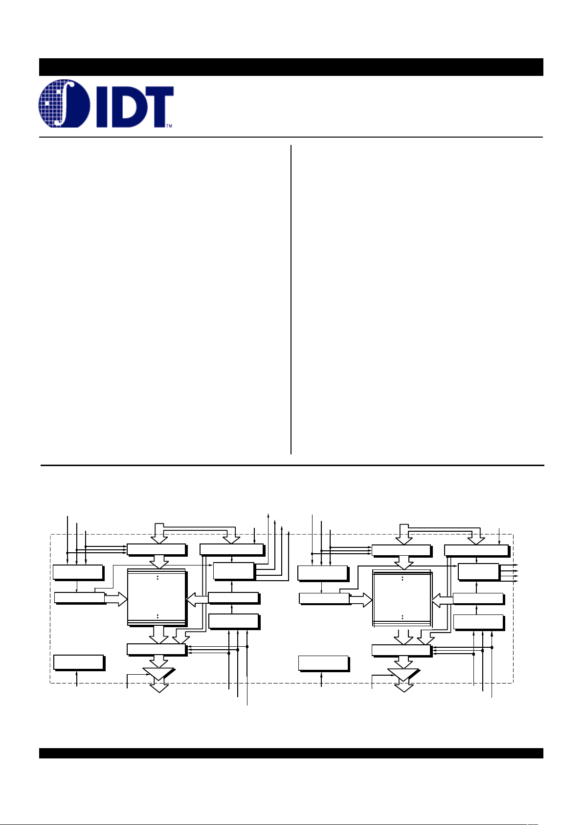
FUNCTIONAL BLOCK DIAGRAM
WCLKA
WENA1
WENA2
DA
0
- DA
8
LDA
OFFSET REGISTERINPUT REGISTER
WRITE CONTROL
LOGIC
RESET LOGIC
OUTPUT REGISTER
OEA
RSA
QA
0
- QA
8
RCLKA
RENA1
RENA2
READ CONTROL
LOGIC
READ POINTER
FLAG
LOGIC
EFA
PAEA
PAFA
FFA
4093 drw 01
WCLKB
WENB1
WENB2
DB
0
- DB
8
LDB
OFFSET REGISTERINPUT REGISTER
RAM ARRAY
256 x 9, 512 x 9,
1,024 x 9, 2,048 x 9,
4,096 x 9, 8,192 x 9
WRITE CONTROL
LOGIC
WRITE POINTER
RESET LOGIC
OUTPUT REGISTER
OEB
RSB
QB
0
- QB
8
RCLKB
RENB1
RENB2
READ CONTROL
LOGIC
READ POINTER
FLAG
LOGIC
EFB
PAFB
FFB
PAEB
WRITE POINTER
RAM ARRAY
256 x 9, 512 x 9,
1,024 x 9, 2,048 x 9,
4,096 x 9, 8,192 x 9
2
IDT72V801/72V811/72V821/72V831/72V841/72V851 COMMERCIAL AND INDUSTRIAL TEMPERATURE RANGE
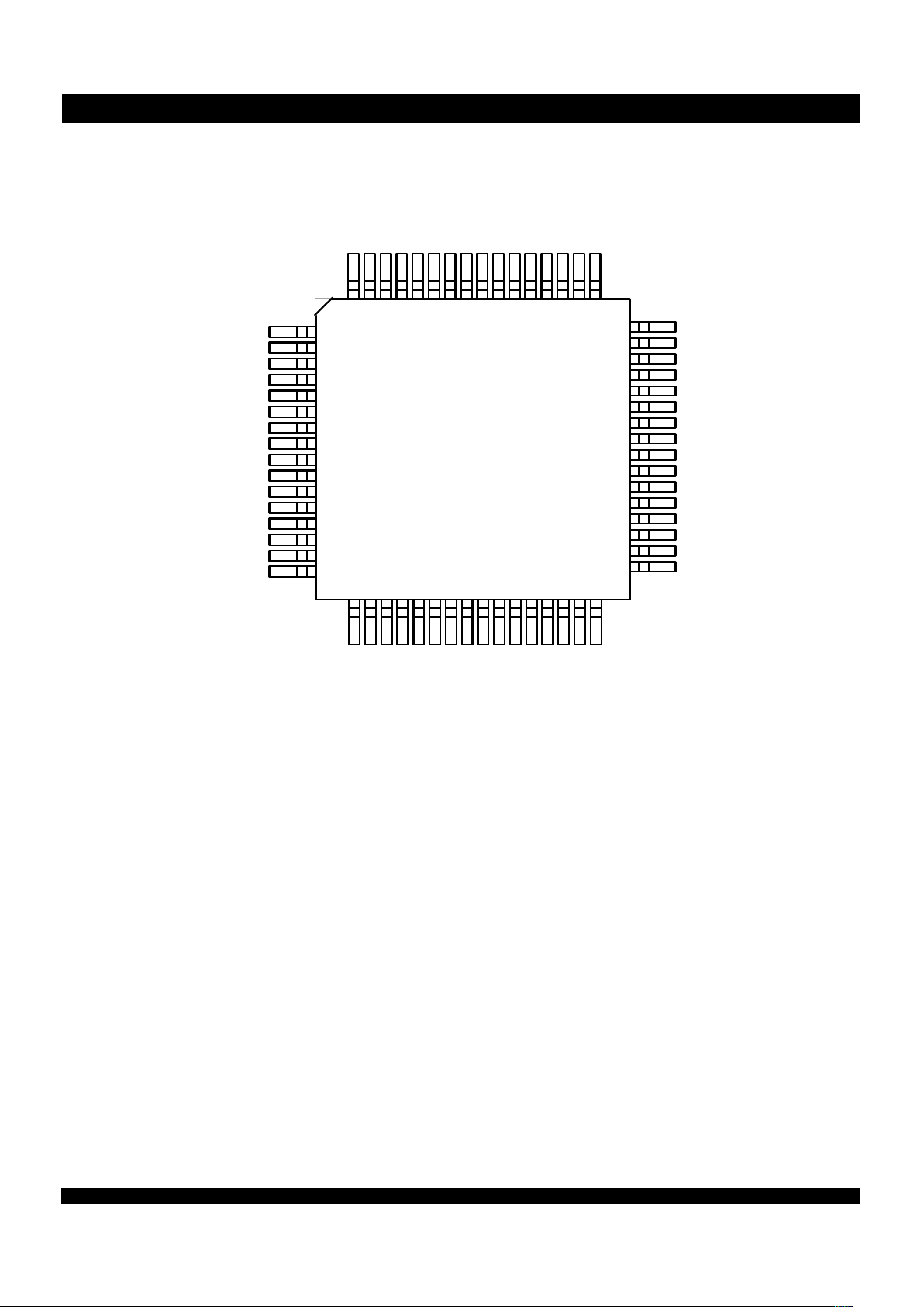
PIN CONFIGURATION
TQFP (PN64-1, order code: PF)
STQFP (PP64-1, order code: TF)
TOP VIEW
QA
1
QA
2
QA
3
QA
4
QA
5
QA
6
QA
7
QA
8
V
CC
WENA2/LDA
WCLKA
WENA
1
RSA
DA
8
DA
7
DA
6
1
2
3
4
5
6
7
8
9
10
11
12
13
14
15
16
QB0
FFB
EFB
OEB
RENB
2
RCLKB
RENB
1
GND
Vcc
PAEB
PAFB
DB
0
DB
1
DB
2
DB
3
DB
4
48
47
46
45
44
43
42
41
40
39
38
37
36
35
34
33
646362616059585756555453525150
49
171819202122232425262728293031
32
QA
0
FFA
EFA
OEA
RENA
2
RCLKA
RENA
1
GND
QB
8QB7QB6QB5QB4QB3QB2QB1
DA5DA4DA3DA
2
DA
1
DA
0
PAFA
PAEA
WENB
2
/LDB
WCLKB
WENB
1
RSB
DB
8
DB
7
DB6DB
5
4093 drw 02
3
IDT72V801/72V811/72V821/72V831/72V841/72V851 COMMERCIAL AND INDUSTRIAL TEMPERATURE RANGE
PIN DESCRIPTIONS
The IDT72V801/72V811/72V821/72V831/72V841/72V851's two FIFOs,
referred to as FIFO A and FIFO B, are identical in every respect. The following
description defines the input and output signals for FIFO A. The corresponding
signal names for FIFO B are provided in parentheses.
Symbol Name I/O Description
DA0-DA8 A Data Inputs I 9-bit data inputs to RAM array A.
D
B0-DB8 B Data Inputs I 9-bit data inputs to RAM array B.
RSA, RSB Reset I When RSA (RSB) is set LOW, the associated internal read and write pointers of array A (B) are set to the first
location; FFA (FFB) and PAFA (PAFB) go HIGH, and PAEA (PAEB) and EFA (EFB) go LOW. After powerup, a reset of both FIFOs A and B is required before an initial WRITE.
WCLKA Write Clock I Data is written into the FIFO A (B) on a LOW-to-HIGH transition of WCLKA (WCLKB) when the write enable(s)
WCLKB are asserted.
WENA1 Write Enable 1 I If FIFO A (B) is configured to have programmable flags, WENA1 (WENB1) is the only write enable pin that can be
WENB1 used. When WENA1 (WENB1) is LOW, data A (B) is written into the FIFO on every LOW-to-HIGH transition
WCLKA (WCLKB). If the FIFO is configured to have two write enables, WENA1 (WENB1) must be LOW and
WENA2 (WENB2) must be HIGH to write data into the FIFO. Data will not be written into the FIFO if FFA (FFB) is
LOW.
WENA2/LDA Write Enable 2/ I FIFO A (B) is configured at reset to have either two write enables or programmable flags. If LDA (LDB) is HIGH at
WENB2/LDB Load reset, this pin operates as a second Write Enable. If WENA2/LDA (WENB2/LDB) is LOW at reset this pin operates
as a control to load and read the programmable flag offsets for its respective array. If the FIFO is configured to have
two write enables, WENA1 (WENB1) must be LOW and WENA2 (WENB2) must be HIGH to write data into FIFO
A (B). Data will not be written into FIFO A (B) if FFA (FFB) is LOW. If the FIFO is configured to have programmable
flags, LDA (LDB) is held LOW to write or read the programmable flag offsets.
Q
A0-QA8 A Data Outputs O 9-bit data outputs from RAM array A.
Q
B0-QB8 B Data Outputs O 9-bit data outputs from RAM array B.
RCLKA Read Clock I Data is read from FIFO A (B) on a LOW-to-HIGH transition of RCLKA (RCLKB) when RENA1(RENB1) and
RCLKB RENA2 (RENB2) are asserted.
RENA1 Read Enable 1 I When RENA1 (RENB1) and RENA2 (RENB2) are LOW, data is read from FIFO A (B) on every LOW-to-HIGH
RENB1 transition of RCLKA (RCLKB). Data will not be read from Array A (B) if EFA (EFB) is LOW.
RENA2 Read Enable 2 I When RENA1 (RENB1) and RENA2 (RENB2) are LOW, data is read from the FIFO A (B) on every LOW-toRENB2 HIGH transition of RCLKA (RCLKB). Data will not be read from array A (B) if the EFA (EFB) is LOW.
OEA Output Enable I When OEA (OEB) is LOW, outputs D
A0-DA8 (DB0-DB8) are active. If OEA (OEB) is HIGH, the OEB outputs DA0 -
D
A8 (DB0-DB8) will be in a high-impedance state.
EFA Empty Flag O When EFA (EFB) is LOW, FIFO A (B) is empty and further data reads from the output are inhibited. When EFA
EFB (EFB) is HIGH, FIFO A (B) is not empty. EFA (EFB) is synchronized to RCLKA (RCLKB).
PAEA Programmable O When PAEA (PAEB) is LOW, FIFO A (B) is Almost-Empty based on the offset programmed into the appropriate
PAEB Almost-Empty Flag offset register. The default offset at reset is Empty+7. PAEA (PAEB) is synchronized to RCLKA (RCLKB).
PAFA Programmable O When PAFA (PAFB) is LOW, FIFO A (B) is Almost-Full based on the offset programmed into the appropriate offset
PAFB Almost-Full Flag register. The default offset at reset is Full-7. PAFA (PAFB) is synchronized to WCLKA (WCLKB).
FFA Full Flag O When FFA (FFB) is LOW, FIFO A (B) is full and further data writes into the input are inhibited. When FFA (FFB) is
FFB HIGH, FIFO A (B) is not full. FFA (FFB) is synchronized to WCLKA (WCLKB).
V
CC Power +3.3V power supply pin.
GND Ground 0V ground pin.
4
IDT72V801/72V811/72V821/72V831/72V841/72V851 COMMERCIAL AND INDUSTRIAL TEMPERATURE RANGE
Symbol Rating Commercial Unit
V
TERM Terminal Voltage with –0.5 to +5 V
Respect to GND
T
STG Storage Temperature –55 to +125
°
C
I
OUT DC Output Current –50 to +50 mA
NOTE:
1. Stresses greater than those listed under ABSOLUTE MAXIMUM RATINGS may cause
permanent damage to the device. This is a stress rating only and functional operation
of the device at these or any other conditions above those indicated in the operational
sections of the specification is not implied. Exposure to absolute maximum rating
conditions for extended periods may affect reliability.
RECOMMENDED OPERATING
CONDITIONS
VCC Supply Voltage(Com’l & Ind’l) 3 .0 3.3 3.6 V
GND Supply Voltage(Com’l & Ind’l) 0 0 — V
V
IH Input High Voltage
(Com’l & Ind’l) 2.0 — 5.0 V
V
IL Input Low Voltage
(Com’l & Ind’l) — — 0.8 V
T
A Operating Temperature 0 — 70
°
C
Commercial
T
A Operating Temperature -40 85
°
C
Industrial
IDT72V801
IDT72V811
IDT72V821
IDT72V831
IDT72V841
IDT72V851
Commercial and Industrial
(1)
tCLK = 10, 15, 20 ns
Symbol Parameter Min. Typ. Max. Unit
I
LI
(2)
Input Leakage Current (Any Input) – 1 — – 1 µA
I
LO
(3)
Output Leakage Current –1 0 — 10 µA
V
OH Output Logic “1” Voltage, IOH = –2 mA 2.4 — — V
V
OL Output Logic “0” Voltage, IOL = 8 mA — — 0.4 V
I
CC1
(4,5,6)
Active Power Supply Current (both FIFOs) — — 40 mA
I
CC2
(3,7)
Standby Current — — 1 0 mA
NOTES:
1.
Industrial temperature range product for the 15ns speed grade is available as a standard device.
2. Measurements with 0.4 ≤ V
IN ≤ VCC.
3. OEA, OEB ≥ V
IH, 0.4 ≤ VOUT ≤ VCC.
4. Tested with outputs disabled (I
OUT = 0).
5. RCLK and WCLK toggle at 20 MHz and data inputs switch at 10 MHz.
6. Typical I
CC1 = 2[0.17 + 0.48*fS + 0.02*CL*fS] (in mA).
These equations are valid under the following conditions:
V
CC = 3.3V, TA = 25°C, fS = WCLK frequency = RCLK frequency (in MHz, using TTL levels), data switching at fS/2, CL = capacitive load (in pF).
7. All Inputs = V
CC - 0.2V or GND + 0.2V, except RCLK and WCLK, which toggle at 20 MHz.
DC ELECTRICAL CHARACTERISTICS
(Commercial: VCC = 3.3V ± 0.3V, TA = 0°C to +70°C; Industrial :VCC = 3.3V ± 0.3V, TA = -40°C to +85°C)
Symbol Parameter Conditions Max. Unit
C
IN
(2)
Input Capacitance VIN = 0V 10 pF
C
OUT
(1,2)
Output Capacitance VOUT = 0V 10 pF
NOTE:
1. With output deselected (OEA, OEB ≥ V
IH).
2. Characterized values, not currently tested.
ABSOLUTE MAXIMUM RATINGS
Symbol Parameter Min Typ. Max Unit
CAPACITANCE (TA = +25
°
C, f = 1.0MHz)
5
IDT72V801/72V811/72V821/72V831/72V841/72V851 COMMERCIAL AND INDUSTRIAL TEMPERATURE RANGE
In Pulse Levels GND to 3.0V
Input Rise/Fall Times 3ns
Input Timing Reference Levels 1.5V
Output Reference Levels 1.5V
Output Load See Figure 1
Commercial Com’l & Ind’l Commercial
IDT72V801L10 IDT72V801L15 IDT72V801L20
IDT72V811L10 IDT72V811L15 IDT72V811L20
IDT72V821L10 IDT72V821L15 IDT72V821L20
IDT72V831L10 IDT72V831L15 IDT72V831L20
IDT72V841L10 IDT72V841L15 IDT72V841L20
IDT72V851L10 IDT72V851L15 IDT72V851L20
Symbol Parameter Min. Max. Min. Max. Min. Max. Unit
f
S Clock Cycle Frequency — 100 — 66.7 — 50 MHz
t
A Data Access Time 2 6. 5 2 10 2 12 ns
t
CLK Clock Cycle Time 10 — 15
(1)
—20—ns
t
CLKH Clock High Time 4.5 — 6 — 8 — ns
t
CLKL Clock Low Time 4.5 — 6 — 8 — ns
t
DS Data Set-up Time 3 — 4 — 5 — ns
t
DH Data Hold Time 0.5 — 1 — 1 — n s
t
ENS Enable Set-up Time 3 — 4 — 5 — ns
t
ENH Enable Hold Time 0.5 — 1 — 1 — ns
t
RS Reset Pulse Width
(2)
10 — 15 — 20 — ns
t
RSS Reset Set-up Time 8 — 10 — 1 2 — ns
t
RSR Reset Recovery Time 8 — 10 — 1 2 — ns
t
RSF Reset to Flag Time and Output Time — 1 0 — 15 — 2 0 n s
t
OLZ Output Enable to Output in Low-Z
(3)
0—0— 0—ns
t
OE Output Enable to Output Valid 3 6 3 8 3 1 0 ns
t
OHZ Output Enable to Output in High-Z
(3)
3638 310ns
t
WFF Write Clock to Full Flag — 6. 5 — 10 — 12 ns
t
REF Read Clock to Empty Flag — 6.5 — 1 0 — 12 ns
t
PAF Write Clock to Programmable Almost-Full Flag — 6. 5 — 1 0 — 1 2 ns
t
PAE Read Clock to Programmable Almost-Empty Flag — 6. 5 — 10 — 1 2 ns
t
SKEW1 Skew Time Between Read Clock and Write Clock 5 — 6 — 8 — n s
for Empty Flag and Full Flag
t
SKEW2 Skew Time Between Read Clock and Write Clock for 14 — 1 8 — 20 — ns
Programmable Almost-Empty Flag and Programmable
Almost-Full Flag
*Includes jig and scope capacitances.
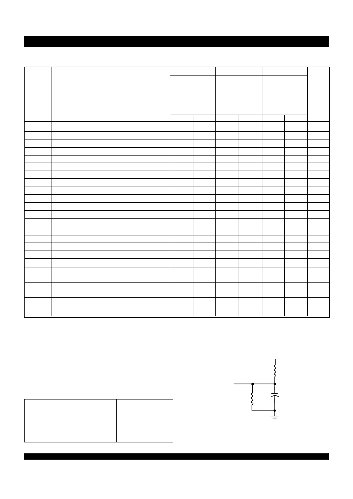
Figure 1. Output Load
or equivalent circuit
NOTES:
1. Industrial temperature range product for the 15ns speed grade is available as a standard device.
2. Pulse widths less than minimum values are not allowed.
3. Values guaranteed by design, not currently tested.
30pF*
330Ω
3.3V
510Ω
D.U.T.
4093 drw 03
AC ELECTRICAL CHARACTERISTICS
(1)
(Commercial: VCC = 3.3V ± 0.3V, TA = 0°C to +70°C; Industrial: VCC = 3.3V± 0.3V, TA = -40°C to +85°C)
AC TEST CONDITIONS
 Loading...