

查询IDT72V2101供应商
3.3 VOLT HIGH DENSITY CMOS
SUPERSYNC FIFO™
262,144 x 9
524,288 x 9
FEATURES:
••
• Choose among the following memory organizations:
••
IDT72V2101
IDT72V2111
•
Pin-compatible with the IDT72V261/72V271 and the IDT72V281/
72V291 SuperSync FIFOs
• 10ns read/write cycle time (6.5ns access time)
• Fixed, low first word data latency time
• 5V input tolerant
• Auto power down minimizes standby power consumption
• Master Reset clears entire FIFO
• Partial Reset clears data, but retains programmable settings
• Retransmit operation with fixed, low first word data latency time
• Empty, Full and Half-Full flags signal FIFO status
• Programmable Almost-Empty and Almost-Full flags, each flag can
default to one of two preselected offsets
• Program partial flags by either serial or parallel means
• Select IDT Standard timing (using EF and FF flags) or First Word Fall
Through timing (using OR and IR flags)
•
Output enable puts data outputs into high impedance state
• Easily expandable in depth and width
• Independent Read and Write clocks (permit reading and writing
262,144 x 9
524,288 x 9
IDT72V2101
IDT72V2111
simultaneously)
• Available in the 64-pin Thin Quad Flat Pack (TQFP)
• High-performance submicron CMOS technology
DESCRIPTION:
The IDT72V2101/72V2111 are exceptionally deep, high speed, CMOS
First-In-First-Out (FIFO) memories with clocked read and write controls. These
FIFOs offer numerous improvements over previous SuperSync FIFOs,
including the following:
• The limitation of the frequency of one clock input with respect to the other has
been removed. The Frequency Select pin (FS) has been removed, thus
it is no longer necessary to select which of the two clock inputs, RCLK or
WCLK, is running at the higher frequency.
• The period required by the retransmit operation is now fixed and short.
• The first word data latency period, from the time the first word is written to an
empty FIFO to the time it can be read, is now fixed and short. (The variable
clock cycle counting delay associated with the latency period found on
previous SuperSync devices has been eliminated on this SuperSync family.)
SuperSync FIFOs are particularly appropriate for network, video, telecommunications, data communications and other applications that need to buffer large
amounts of data.
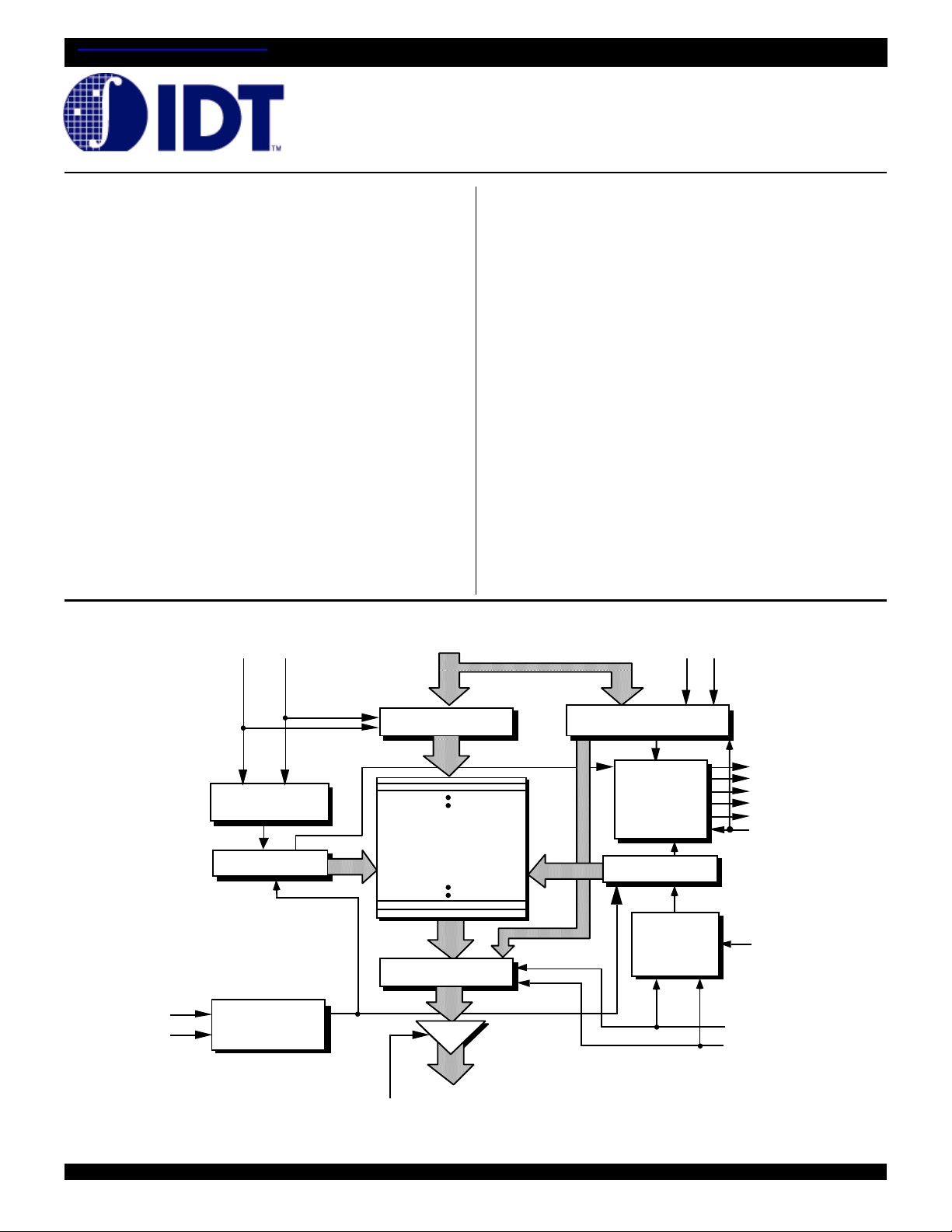
FUNCTIONAL BLOCK DIAGRAM
WEN
WCLK
WRITE CONTROL
LOGIC
WRITE POINTER
OUTPUT REGISTER
MRS
PRS
RESET
LOGIC
0
-D
8
D
INPUT REGISTER
RAM ARRAY
262,144 x 9
524,288 x 9
LD
OFFSET REGISTER
FLAG
LOGIC
READ POINTER
READ
CONTROL
LOGIC
SEN
FF/IR
PAF
EF/OR
PAE
HF
FWFT/SI
RT
RCLK
REN
0
-Q
8
OE
The SuperSync FIFO is a trademark and the IDT logo is a registered trademark of Integrated Device Technology, Inc.
COMMERCIAL AND INDUSTRIAL TEMPERATURE RANGES
2001 Integrated Device Technology, Inc.
Q
4669 drw 01
MARCH 2001
DSC-4669/2
IDT72V2101/72V2111 3.3V HIGH DENSITY CMOS
SUPERSYNC FIFO
TM
262,144 x 9, 524,288 x 9
COMMERCIAL AND INDUSTRIAL
TEMPERATURE RANGES
DESCRIPTION (CONTINUED)
The input port is controlled by a Write Clock (WCLK) input and a Write Enable
(WEN) input. Data is written into the FIFO on every rising edge of WCLK when
WEN is asserted. The output port is controlled by a Read Clock (RCLK) input
and Read Enable (REN) input. Data is read from the FIFO on every rising edge
of RCLK when REN is asserted. An Output Enable (OE) input is provided for
three-state control of the outputs.
The frequencies of both the RCLK and the WCLK signals may vary from
0 to f
MAX with complete independence. There are no restrictions on the
frequency of the one clock input with respect to the other.
There are two possible timing modes of operation with these devices:
IDT Standard mode and First Word Fall Through (FWFT) mode.
In IDT Standard mode, the first word written to an empty FIFO will not
appear on the data output lines unless a specific read operation is
performed. A read operation, which consists of activating REN and enabling a
rising RCLK edge, will shift the word from internal memory to the data output lines.
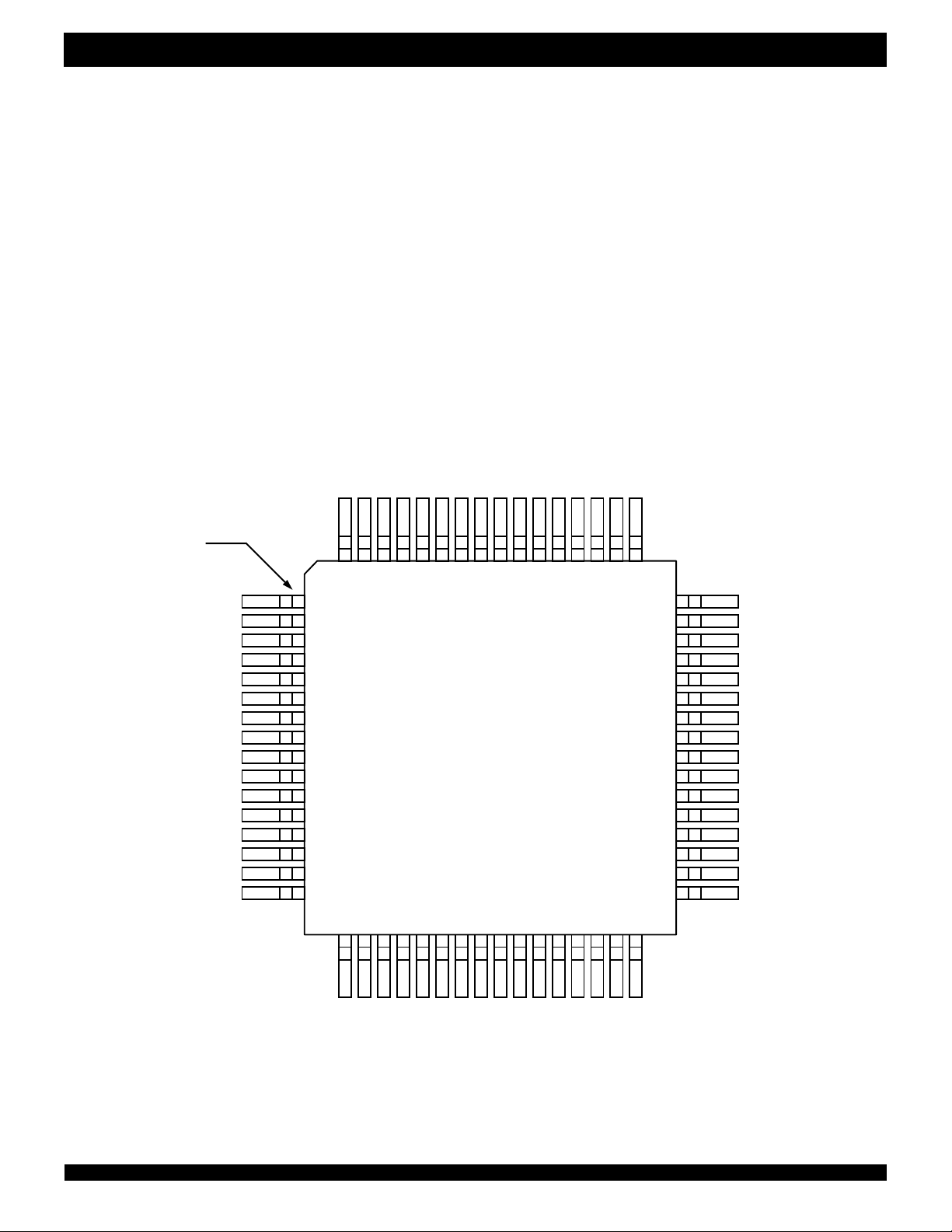
PIN CONFIGURATIONS
FWFT/SI
WCLK
PRS
MRS
LD
GND
In FWFT mode, the first word written to an empty FIFO is clocked directly
to the data output lines after three transitions of the RCLK signal. A REN
does not have to be asserted for accessing the first word. However,
subsequent words written to the FIFO do require a LOW on REN for access.
The state of the FWFT/SI input during Master Reset determines the timing
mode in use.
For applications requiring more data storage capacity than a single FIFO
can provide, the FWFT timing mode permits depth expansion by chaining
FIFOs in series (i.e. the data outputs of one FIFO are connected to the
corresponding data inputs of the next). No external logic is required.
These FIFOs have five flag pins, EF/OR (Empty Flag or Output Ready),
FF/IR (Full Flag or Input Ready), HF (Half-full Flag), PAE (Programmable
Almost-Empty flag) and PAF (Programmable Almost-Full flag). The EF and
FF functions are selected in IDT Standard mode. The IR and OR functions are
selected in FWFT mode. HF, PAE and PAF are always available for use,
irrespective of timing mode.
CC
PAF
HF
V
EF/OR
PAE
RCLK
REN
OE
RT
FF/IR
PIN 1
WEN
SEN
DC
V
V
GND
GND
GND
GND
GND
GND
GND
GND
GND
CC
CC
D8
D7
64 63 62 61 60 59 58 57 56 55 54 53 52 51 50 49
(3)
1
2
(1)
3
4
5
(2)
(2)
(2)
(2)
(2)
(2)
(2)
(2)
(2)
6
7
8
9
10
11
12
13
14
15
16
48
47
46
45
44
43
42
41
40
39
38
37
36
35
34
33
DNC
DNC
GND
DNC
DNC
V
CC
DNC
DNC
DNC
GND
DNC
DNC
Q8
Q7
Q6
GND
(3)
(3)
(3)
(3)
(3)
(3)
(3)
(3)
17 18 19 20 21 22 23 24 25 26 27 28 29 30 31 32
NOTES:
1. DC = Don’t Care. Must be tied to GND or V
2. This pin may either be tied to ground or left open.
3. DNC = Do Not Connect.
CC, cannot be left open.
D6
D5
D4
D3
D2
D1
GND
D0
TQFP (PN64-1, order code: PF)
TOP VIEW
2
Q0
Q1
GND
Q2
Q3
CC
V
Q4
Q5
4669 drw 02

IDT72V2101/72V2111 3.3V HIGH DENSITY CMOS
SUPERSYNC FIFO
TM
262,144 x 9, 524,288 x 9
COMMERCIAL AND INDUSTRIAL
TEMPERATURE RANGES
PAE and PAF can be programmed independently to switch at any point in
memory. (See Table I and Table II.) Programmable offsets determine the flag
switching threshold and can be loaded by two methods: parallel or serial. Two
default offset settings are also provided, so that PAE can be set to switch at 127
or 1,023 locations from the empty boundary and the PAF threshold can be set
at 127 or 1,023 locations from the full boundary. These choices are made with
the LD pin during Master Reset.
For serial programming, SEN together with LD on each rising edge of
WCLK, are used to load the offset registers via the Serial Input (SI). For
parallel programming, WEN together with LD on each rising edge of WCLK,
are used to load the offset registers via D
n. REN together with LD on each
rising edge of RCLK can be used to read the offsets in parallel from Qn
regardless of whether serial or parallel offset loading has been selected.
During Master Reset (MRS) the following events occur: The read and write
pointers are set to the first location of the FIFO. The FWFT pin selects IDT
Standard mode or FWFT mode. The LD pin selects either a partial flag default
setting of 127 with parallel programming or a partial flag default setting of 1,023
with serial programming. The flags are updated according to the timing mode
and default offsets selected.
The Partial Reset (PRS) also sets the read and write pointers to the first
location of the memory. However, the timing mode, partial flag programming method, and default or programmed offset settings existing before
Partial Reset remain unchanged. The flags are updated according to the
timing mode and offsets in effect. PRS is useful for resetting a device in midoperation, when reprogramming partial flags would be undesirable.
The Retransmit function allows data to be reread from the FIFO. A LOW
on the RT input during a rising RCLK edge initiates a retransmit operation
by setting the read pointer to the first location of the memory array.
If, at any time, the FIFO is not actively performing an operation, the chip will
automatically power down. Once in the power down state, the standby supply
current consumption is minimized. Initiating any operation (by activating control
inputs) will immediately take the device out of the power down state.
The IDT72V2101/72V2111 are fabricated using IDT’s high speed submicron CMOS technology.
PARTIAL RESET (PRS)
WRITE CLOCK (WCLK)
WRITE ENABLE (WEN)
LOAD (LD)
0
DATA IN (D
- Dn)
SERIAL ENABLE(SEN)
FIRST WORD FALL THROUGH/SERIAL INPUT
(FWFT/SI)
FULL FLAG/INPUT READY (FF/IR)
PROGRAMMABLE ALMOST-FULL (PAF)
Figure 1. Block Diagram of Single 262,144 x 9 and 524,288 x 9 Synchronous FIFO
MASTER RESET (MRS)
READ CLOCK (RCLK)
READ ENABLE (REN)
OUTPUT ENABLE (OE)
DATA OUT (Q0 - Qn)
IDT
72V2101
72V2111
RETRANSMIT (RT)
EMPTY FLAG/OUTPUT READY (EF/OR)
PROGRAMMABLE ALMOST-EMPTY (PAE)
HALF FULL FLAG (HF)
4669 drw 03
3

IDT72V2101/72V2111 3.3V HIGH DENSITY CMOS
SUPERSYNC FIFO
TM
262,144 x 9, 524,288 x 9
COMMERCIAL AND INDUSTRIAL
TEMPERATURE RANGES
PIN DESCRIPTION
Symbol Name I/O Description
0–D8 Data Inputs I Data inputs for a 9-bit bus.
D
MRS Master Reset I MRS initializes the read and write pointers to zero and sets the output register to
all zeroes. During Master Reset, the FIFO is configured for either FWFT or IDT
Standard mode, one of two programmable flag default settings, and serial or
parallel programming of the offset settings.
PRS Partial Reset I PRS initializes the read and write pointers to zero and sets the output register to
all zeroes. During Partial Reset, the existing mode (IDT or FWFT), programming
method (serial or parallel), and programmable flag settings are all retained.
RT Retransmit I RT asserted on the rising edge of RCLK initializes the READ pointer to zero, sets
the EF flag to LOW (OR to HIGH in FWFT mode) temporarily and does not disturb
the write pointer, programming method, existing timing mode or programmable flag
settings. RT is useful to reread data from the first physical location of the FIFO.
FWFT/SI First Word Fall I During Master Reset, selects First Word Fall Through or IDT Standard mode.
Through/Serial In After Master Reset, this pin functions as a serial input for loading offset registers
WCLK Write Clock I When enabled by WEN, the rising edge of WCLK writes data into the FIFO and
offsets into the programmable registers for parallel programming, and when
enabled by SEN, the rising edge of WCLK writes one bit of data into the
programmable register for serial programming.
WEN Write Enable I WEN enables WCLK for writing data into the FIFO memory and offset registers.
RCLK Read Clock I When enabled by REN, the rising edge of RCLK reads data from the FIFO
memory and offsets from the programmable registers.
REN Read Enable I REN enables RCLK for reading data from the FIFO memory and offset registers.
OE Output Enable I OE controls the output impedance of Q
SEN Serial Enable I SEN enables serial loading of programmable flag offsets.
LD Load I During Master Reset, LD selects one of two partial flag default offsets (127 or
1,023) and determines the flag offset programming method, serial or parallel. After
Master Reset, this pin enables writing to and reading from the offset registers.
DC Don't Care I This pin must be tied to either V
Reset.
FF/IR Full Flag/ O In the IDT Standard mode, the FF function is selected. FF indicates whether or
Input Ready not the FIFO memory is full. In the FWFT mode, the IR function is selected. IR
indicates whether or not there is space available for writing to the FIFO memory.
EF/OR Empty Flag/ O In the IDT Standard mode, the EF function is selected. EF indicates whether or
Output Ready not the FIFO memory is empty. In FWFT mode, the OR function is selected.
OR indicates whether or not there is valid data available at the outputs.
PAF Programmable O PAF goes LOW if the number of words in the FIFO memory is more than
Almost-Full Flag total word capacity of the FIFO minus the full offset value m, which is stored in the
Full Offset register. There are two possible default values for m: 127 or 1,023.
PAE Programmable O PAE goes LOW if the number of words in the FIFO memory is less than offset n,
Almost-Empty Flag which is stored in the Empty Offset register. There are two possible default values
for n: 127 or 1,023. Other values for n can be programmed into the device.
HF Half-Full Flag O HF indicates whether the FIFO memory is more or less than half-full.
Q
0–Q8 Data Outputs O Data outputs for a 9-bus
V
CC Power +3.3 Volt power supply pins.
GND Ground Ground pins.
n.
CC or GND and must not toggle after Master
4
IDT72V2101/72V2111 3.3V HIGH DENSITY CMOS
SUPERSYNC FIFO
TM
262,144 x 9, 524,288 x 9
COMMERCIAL AND INDUSTRIAL
TEMPERATURE RANGES
ABSOLUTE MAXIMUM RATINGS
Symbol Rating Com’l & Ind’l Unit
(2)
TERM
V
T
STG Storage –55 to +125 °C
OUT DC Output Current –50 to +50 mA
I
NOTES:
1. Stresses greater than those listed under ABSOLUTE MAXIMUM RATINGS may cause
permanent damage to the device. This is a stress rating only and functional operation
of the device at these or any other conditions above those indicated in the operational
sections of this specification is not implied. Exposure to absolute maximum rating
conditions for extended periods may affect reliability.
CC terminal only.
2. V
Terminal Voltage –0.5 to +4.5 V
with respect to GND
Temperature
RECOMMENDED DC OPERATING
CONDITIONS
Symbol Parameter Min. Typ. Max. Unit
(1)
V
CC
Supply Voltage (Com'l & Ind'l) 3.15 3.3 3.45 V
GND Supply Voltage (Com'l & Ind'l) 0 0 0 V
IH Input High Voltage (Com'l & Ind'l) 2.0 — 5.5 V
V
(2)
IL
Input Low Voltage (Com'l & Ind'l) — — 0.8 V
V
A Operating Temperature Commercial 0 — +70 ° C
T
A Operating Temperature Industrial - 40 — +85 °C
T
NOTES:
CC = 3.3V ± 0.15V, JEDEC JESD8-A compliant.
1. V
2. 1.5V undershoots are allowed for 10ns once per cycle.
DC ELECTRICAL CHARACTERISTICS
(Commercial: VCC = 3.3V ± 0.15V, TA = 0°C to +70°C; Industrial: VCC = 3.3V ± 0.15V, TA = -40°C to +85°C; JEDEC JESD8-A compliant)
IDT72V2101L
IDT72V2111L
Commercial and Industrial
tCLK = 10, 15, 20 ns
Symbol Parameter Min. Max. Unit
(2)
I
LI
(3)
LO
I
V
OH Output Logic “1” Voltage, IOH = –2 mA 2.4 — V
OL Output Logic “0” Voltage, IOL = 8 mA — 0.4 V
V
(4,5,6)
I
CC1
(4,7)
CC2
I
NOTES:
1. Industrial temperature range product for the 15ns speed grade is available as a standard device.
2. Measurements with 0.4 ≤ V
3. OE
≥ VIH, 0.4 ≤ VOUT ≤ VCC.
4. Tested with outputs open (IOUT = 0).
5. RCLK and WCLK toggle at 20 MHz and data inputs switch at 10 MHz.
6. Typical I
L = capacitive load (in pF).
C
7. All Inputs = V
Input Leakage Current –1 1 µA
Output Leakage Current –1 0 10 µA
Active Power Supply Current — 5 5 mA
Standby Current — 20 mA
IN ≤ VCC.
CC1 = XX + XX*fS + 0.02*CL*fS (in mA) with VCC = 3.3V, tA = 25°C, fS = WCLK frequency = RCLK frequency (in MHz, using TTL levels), data switching at fS/2,
CC - 0.2V or GND + 0.2V, except RCLK and WCLK, which toggle at 20 MHz.
(1)
CAPACITANCE (TA = +25°C, f = 1.0MHz)
Symbol Parameter
(2)
IN
C
Input VIN = 0V 10 pF
Capacitance
(1,2)
C
OUT
Output VOUT = 0V 10 pF
Capacitance
NOTES:
1. With output deselected, (OE ≥ V
2. Characterized values, not currently tested.
(1)
Conditions Max. Unit
IH).
5
IDT72V2101/72V2111 3.3V HIGH DENSITY CMOS
SUPERSYNC FIFO
TM
262,144 x 9, 524,288 x 9
COMMERCIAL AND INDUSTRIAL
TEMPERATURE RANGES
AC ELECTRICAL CHARACTERISTICS
(1)
(Commercial: VCC = 3.3V ± 0.15V, TA = 0°C to +70°C; Industrial: VCC = 3.3V ± 0.15V, TA = -40°C to +85°C; JEDEC JESD8-A compliant)
Commercial Com’l & Ind’l
IDT72V2101L10 IDT72V2101L15 IDT72V2101L20
IDT72V2111L10 IDT72V2111L15 IDT72V2111L20
Symbol Parameter Min. Max. Min. Max. Min. Max. Unit
S Clock Cycle Frequency — 100 — 66.7 — 50 MHz
f
A Data Access Time 2 6.5 2 1 0 2 12 ns
t
CLK Clock Cycle Time 10 — 15 — 20 — ns
t
CLKH Clock High Time 4.5 — 6 — 8 — ns
t
CLKL Clock Low Time 4.5 — 6 — 8 — ns
t
DS Data Setup Time 3 — 4 — 5 — ns
t
DH Data Hold Time 0.5 — 1 — 1 — ns
t
ENS Enable Setup Time 3 — 4 — 5 — ns
t
ENH Enable Hold Time 0. 5 — 1 — 1 — ns
t
LDS Load Setup Time 3 — 4 — 5 — ns
t
LDH Load Hold Time 0 .5 — 1 — 1 — n s
t
RS Reset Pulse Width
t
RSS Reset Setup Time 1 5 — 15 — 20 — ns
t
RSR Reset Recovery Time 1 0 — 15 — 2 0 — ns
t
RSF Reset to Flag and Output Time — 10 — 1 5 — 20 ns
t
FWFT Mode Select Time 0 — 0 — 0 — n s
t
RTS Retransmit Setup Time 3 — 4 — 5 — ns
t
OLZ Output Enable to Output in Low Z
t
OE Output Enable to Output Valid 2 6 2 8 2 10 ns
t
OHZ Output Enable to Output in High Z
t
WFF Write Clock to FF or IR — 6.5 — 10 — 12 ns
t
REF Read Clock to EF or OR — 6.5 — 10 — 12 ns
t
PAF Write Clock to PAF — 6.5 — 10 — 12 ns
t
PAE Read Clock to PAE — 6.5 — 10 — 12 ns
t
HF Clock to HF —16—20—22ns
t
SKEW1 Skew time between RCLK and WCLK 8 — 9 — 10 — n s
t
(3)
(4)
(4)
10 — 15 — 20 — ns
0—0—0—ns
2628210ns
for EF/OR and FF/IR
SKEW2 Skew time between RCLK and WCLK 12 — 14 — 15 — ns
t
for PAE and PAF
NOTES:
1. Industrial temperature range product for the 15ns speed grade is available as a standard device.
2. All AC timings apply to both Standard IDT mode and First Word Fall Through mode.
3. Pulse widths less than minimum values are not allowed.
4. Values guaranteed by design, not currently tested.
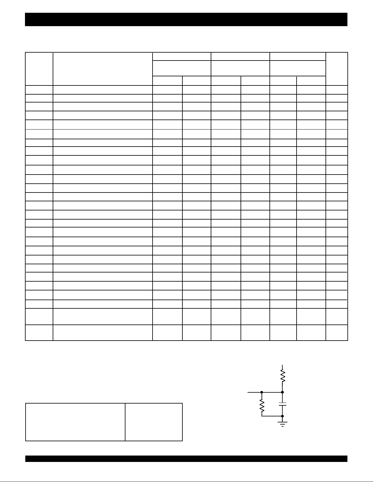
(1)
Commercial
3.3V
330Ω
AC TEST CONDITIONS
Input Pulse Levels GND to 3.0V
Input Rise/Fall Times 3ns
Input Timing Reference Levels 1.5V
Output Reference Levels 1.5V
Output Load See Figure 2
D.U.T.
510Ω
30pF*
4669 drw 04
Figure 2. Output Load
* Includes jig and scope capacitances.
6

IDT72V2101/72V2111 3.3V HIGH DENSITY CMOS
SUPERSYNC FIFO
TM
262,144 x 9, 524,288 x 9
COMMERCIAL AND INDUSTRIAL
TEMPERATURE RANGES
FUNCTIONAL DESCRIPTION
TIMING MODES: IDT STANDARD vs FIRST WORD FALL THROUGH
(FWFT) MODE
The IDT72V2101/72V2111 support two different timing modes of operation:
IDT Standard mode or First Word Fall Through (FWFT) mode. The selection
of which mode will operate is determined during Master Reset, by the state of
the FWFT/SI input.
If, at the time of Master Reset, FWFT/SI is LOW, then IDT Standard mode
will be selected. This mode uses the Empty Flag (EF) to indicate whether or
not there are any words present in the FIFO. It also uses the Full Flag function
(FF) to indicate whether or not the FIFO has any free space for writing. In IDT
Standard mode, every word read from the FIFO, including the first, must be
requested using the Read Enable (REN) and RCLK.
If, at the time of Master Reset, FWFT/SI is HIGH, then FWFT mode will
be selected. This mode uses Output Ready (OR) to indicate whether or not
there is valid data at the data outputs (Q
indicate whether or not the FIFO has any free space for writing. In the FWFT
mode, the first word written to an empty FIFO goes directly to Qn after three
RCLK rising edges, REN = LOW is not necessary. Subsequent words must
be accessed using the Read Enable (REN) and RCLK.
Various signals, both input and output signals operate differently de-
pending on which timing mode is in effect.
IDT STANDARD MODE
In this mode, the status flags, FF, PAF, HF, PAE, and EF operate in the
manner outlined in Table 1. To write data into to the FIFO, Write Enable (WEN)
must be LOW. Data presented to the DATA IN lines will be clocked into the FIFO
on subsequent transitions of the Write Clock (WCLK). After the first write is
performed, the Empty Flag (EF) will go HIGH. Subsequent writes will continue
to fill up the FIFO. The Programmable Almost-Empty flag (PAE) will go HIGH
after n + 1 words have been loaded into the FIFO, where n is the empty offset
value. The default setting for this value is stated in the footnote of Table 1. This
parameter is also user programmable. See section on Programmable Flag
Offset Loading.
If one continued to write data into the FIFO, and we assumed no read
operations were taking place, the Half-Full flag (HF) would toggle to LOW
once the 131,073th word for IDT72V2101 and 262,145th word for
IDT72V2111 respectively was written into the FIFO. Continuing to write
data into the FIFO will cause the Programmable Almost-Full flag (PAF) to
go LOW. Again, if no reads are performed, the PAF will go LOW after
(262,144-m) writes for the IDT72V2101 and (524,288-m) writes for the
IDT72V2111. The offset “m” is the full offset value. The default setting for
this value is stated in the footnote of Table 1. This parameter is also user
programmable. See section on Programmable Flag Offset Loading.
When the FIFO is full, the Full Flag (FF) will go LOW, inhibiting further
write operations. If no reads are performed after a reset, FF will go LOW
after D writes to the FIFO. D = 262,144 writes for the IDT72V2101 and 524,288
for the IDT72V2111, respectively.
n). It also uses Input Ready (IR) to
If the FIFO is full, the first read operation will cause FF to go HIGH.
Subsequent read operations will cause PAF and HF to go HIGH at the conditions
described in Table 1. If further read operations occur, without write operations,
PAE will go LOW when there are n words in the FIFO, where n is the empty
offset value. Continuing read operations will cause the FIFO to become empty.
When the last word has been read from the FIFO, the EF will go LOW inhibiting
further read operations. REN is ignored when the FIFO is empty.
When configured in IDT Standard mode, the EF and FF outputs are double
register-buffered outputs.
Relevant timing diagrams for IDT Standard mode can be found in Figure
7, 8 and 11.
FIRST WORD FALL THROUGH MODE (FWFT)
In this mode, the status flags, IR, PAF, HF, PAE, and OR operate in the
manner outlined in Table 2. To write data into to the FIFO, WEN must be
LOW. Data presented to the DATA IN lines will be clocked into the FIFO on
subsequent transitions of WCLK. After the first write is performed, the
Output Ready (OR) flag will go LOW. Subsequent writes will continue to fill
up the FIFO. PAE will go HIGH after n + 2 words have been loaded into the
FIFO, where n is the empty offset value. The default setting for this value
is stated in the footnote of Table 2. This parameter is also user programmable. See section on Programmable Flag Offset Loading.
If one continued to write data into the FIFO, and we assumed no read
operations were taking place, the HF would toggle to LOW once the
131,074th word for the IDT72V2101 and 262,146th word for the IDT72V2111,
respectively was written into the FIFO. Continuing to write data into the
FIFO will cause the PAF to go LOW. Again, if no reads are performed, the
PAF will go LOW after (262,145-m) writes for the IDT72V2101 and
(524,289-m) writes for the IDT72V2111, where m is the full offset value. The
default setting for this value is stated in the footnote of Table 2.
When the FIFO is full, the Input Ready (IR) flag will go HIGH, inhibiting
further write operations. If no reads are performed after a reset, IR will go HIGH
after D writes to the FIFO. D = 262,145 writes for the IDT72V2101 and 524,289
writes for the IDT72V2111, respectively. Note that the additional word in FWFT
mode is due to the capacity of the memory plus output register.
If the FIFO is full, the first read operation will cause the IR flag to go LOW.
Subsequent read operations will cause the PAF and HF to go HIGH at the
conditions described in Table 2. If further read operations occur, without
write operations, the PAE will go LOW when there are n + 1 words in the
FIFO, where n is the empty offset value. Continuing read operations will
cause the FIFO to become empty. When the last word has been read from
the FIFO, OR will go HIGH inhibiting further read operations. REN is ignored
when the FIFO is empty.
When configured in FWFT mode, the OR flag output is triple registerbuffered, and the IR flag output is double register-buffered.
Relevant timing diagrams for FWFT mode can be found in Figure 9, 10
and 12.
7
IDT72V2101/72V2111 3.3V HIGH DENSITY CMOS
SUPERSYNC FIFO
TM
262,144 x 9, 524,288 x 9
COMMERCIAL AND INDUSTRIAL
TEMPERATURE RANGES
PROGRAMMING FLAG OFFSETS
Full and Empty Flag offset values are user programmable. The IDT72V2101/
72V2111 has internal registers for these offsets. Default settings are stated in the
footnotes of Table 1 and Table 2. Offset values can be programmed into the FIFO
in one of two ways; serial or parallel loading method. The selection of the loading
method is done using the LD (Load) pin. During Master Reset, the state of the
LD input determines whether serial or parallel flag offset programming is
enabled. A HIGH on LD during Master Reset selects serial loading of offset
values and in addition, sets a default PAE offset value of 3FFH (a threshold 1,023
words from the empty boundary), and a default PAF offset value of 3FFH (a
threshold 1,023 words from the full boundary). A LOW on LD during Master
offset value of 07FH (a threshold 127 words from the empty boundary), and
a default PAF offset value of 07FH (a threshold 127 words from the full
boundary). See Figure 3, Offset Register Location and Default Values.
In addition to loading offset values into the FIFO, it also possible to read the
current offset values. It is only possible to read offset values via parallel read.
Figure 4, Programmable Flag Offset Programming Sequence, summarizes the control pins and sequence for both serial and parallel programming
modes. For a more detailed description, see discussion that follows.
The offset registers may be programmed (and reprogrammed) any time
after Master Reset, regardless of whether serial or parallel programming
has been selected.
Reset selects parallel loading of offset values, and in addition, sets a default PAE
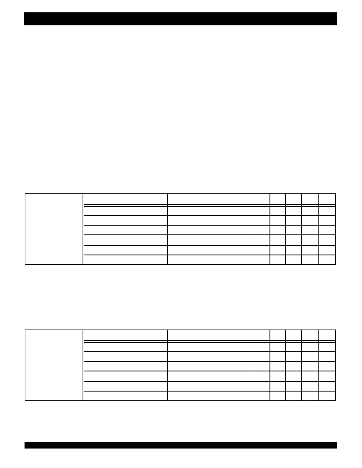
TABLE I STATUS FLAGS FOR IDT STANDARD MODE
IDT72V2101 IDT72V2111
Number of
Words in
FIFO
0
(1)
1 to n
(n+1) to 131,072
131,073 to (262,144-(m+1))
(2)
(262,144-m)
to 262,143
262,144
262,145 to (524,288-(m+1))
(524,288-m)
0
1 to n
(n+1) to 262,144
(2)
524,288
(1)
to 524,287
FF PAF HF PAE EF
HHHL L
HHHLH
HHHHH
HHLHH
HLLHH
LLLHH
NOTES:
1. n = Empty Offset, Default Values: n = 127 when parallel offset loading is selected or n = 1,023 when serial offset loading is selected.
2. m = Full Offset, Default Values: m = 127 when parallel offset loading is selected or m = 1,023 when serial offset loading is selected.
TABLE II STATUS FLAGS FOR FWFT MODE
IDT72V2101 IDT72V2111
0
(1)
to 262,144
(2)
262,146 to (524,289-(m+1))
(524,289-m)
Number of
Words in
FIFO
1 to n+1
(n+2) to 131,073
131,074 to (262,145-(m+1))
(262,145-m)
262,145
NOTES:
1. n = Empty Offset, Default Values: n = 127 when parallel offset loading is selected or n = 1,023 when serial offset loading is selected.
2. m = Full Offset, Default Values: m = 127 when parallel offset loading is selected or m = 1,023 when serial offset loading is selected.
0
1 to n+1
(1)
(n+2) to 262,145
to 524,288
524,289
(2)
IR PAF HF PAE OR
LHHLH
LHHLL
LHHHL
LHLHL
LLLHL
HLL HL
4669 drw 05
8
IDT72V2101/72V2111 3.3V HIGH DENSITY CMOS
SUPERSYNC FIFO
TM
262,144 x 9, 524,288 x 9
COMMERCIAL AND INDUSTRIAL
TEMPERATURE RANGES
IDT72V2101 (262,144 x 9BIT)
87 0
EMPTY OFFSET (LSB) REGISTER
DEFAULT VALUE
7FH if LD is LOW at Master Reset
FFH if LD is HIGH at Master Reset
87 0
EMPTY OFFSET (MID-BYTE) REGISTER
DEFAULT VALUE
00H if LD is LOW at Master Reset
03H if LD is HIGH at Master Reset
821
EMPTY OFFSET
(MSB) REGISTER
DEFAULT
0H
7
8
FULL OFFSET (LSB) REGISTER
DEFAULT VALUE
7FH if LD is LOW at Master Reset
FFH if LD is HIGH at Master Reset
0
83
0
IDT72V2111 (524,288 x 9BIT)
87 0
EMPTY OFFSET (LSB) REGISTER
DEFAULT VALUE
7FH if LD is LOW at Master Reset
FFH if LD is HIGH at Master Reset
87 0
EMPTY OFFSET (MID-BYTE) REGISTER
DEFAULT VALUE
00H if LD is LOW at Master Reset
03H if LD is HIGH at Master Reset
2
EMPTY OFFSET
(MSB) REGISTER
DEFAULT
0H
87 0
FULL OFFSET (LSB) REGISTER
DEFAULT VALUE
7FH if LD is LOW at Master Reset
FFH if LD is HIGH at Master Reset
0
87
FULL OFFSET (MID-BYTE) REGISTER
DEFAULT VALUE
00H if LD is LOW at Master Reset
03H if LD is HIGH at Master Reset
821
FULL OFFSET
(MSB) REGISTER
DEFAULT
0H
0
0
8
Figure 3. Offset Register Location and Default Values
7
8
FULL OFFSET (MID-BYTE) REGISTER
DEFAULT VALUE
00H if LD is LOW at Master Reset
03H if LD is HIGH at Master Reset
0
302
FULL OFFSET
(MSB) REGISTER
DEFAULT
0H
4669 drw 06
9
 Loading...