

Integrated Device Technology Inc IDT723613L15PF, IDT723613L15PQF, IDT723613L20PF, IDT723613L20PQF, IDT723613L30PF Datasheet
...
Integrated Device Technology, Inc.
CMOS Clocked FIFO
With Bus Matching and Byte Swapping
64 x 36
IDT723613
FEATURES:
• Free-running CLKA and CLKB may be asynchronous or
coincident (permits simultaneous reading and writing of
data on a single clock edge)
• 64 x 36 storage capacity FIFO buffering data from Port A
to Port B
• Mailbox bypass registers in each direction
• Dynamic Port B bus sizing of 36-bits (long word), 18-bits
(word), and 9-bits (byte)
• Selection of Big- or Little-Endian format for word and byte
bus sizes
• Three modes of byte-order swapping on Port B
• Programmable Almost-Full and Almost-Empty flags
• Microprocessor interface control logic
•FF, AF flags synchronized by CLKA
•EF, AE flags synchronized by CLKB
• Passive parity checking on each Port
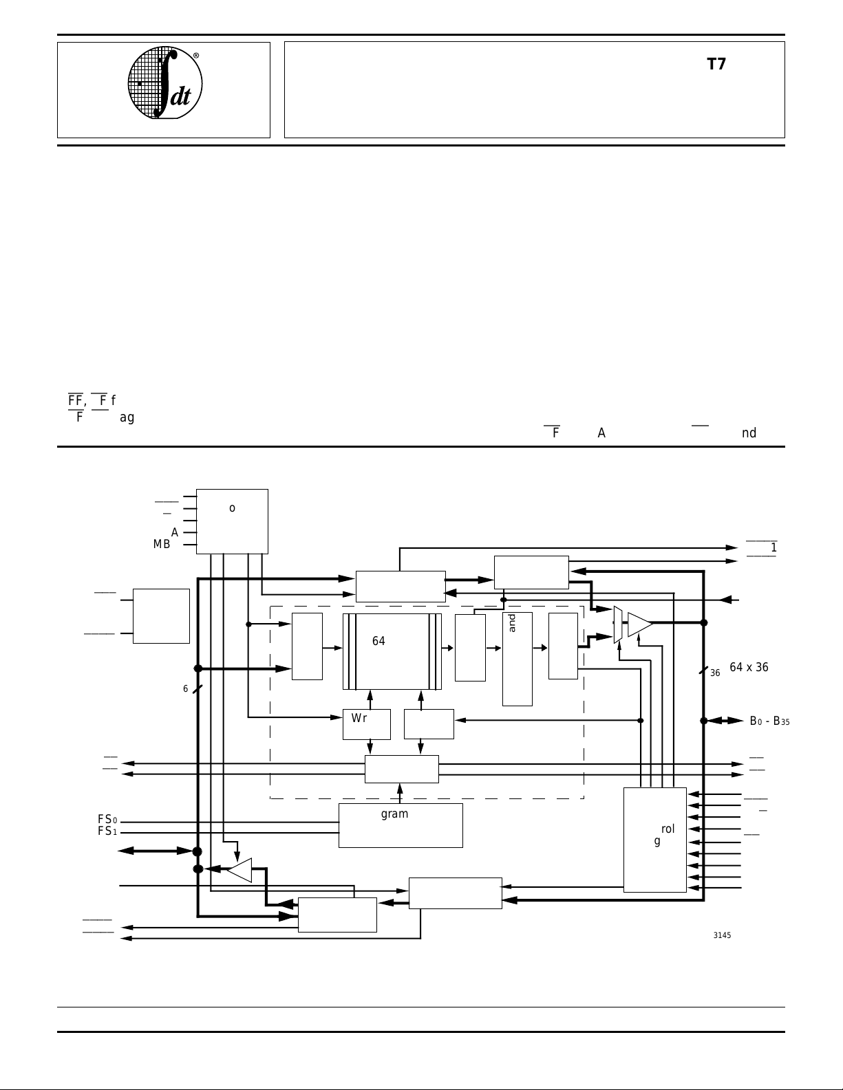
FUNCTIONAL BLOCK DIAGRAM
RST
ODD/
EVEN
CLKA
CSA
W/RA
ENA
MBA
Device
Control
36
Port-A
Control
Logic
Input
Register
Mail 1
Register
64 x 36
SRAM
Write
Pointer
• Parity Generation can be selected for each Port
• Low-power advanced BiCMOS technology
• Supports clock frequencies up to 67 MHz
• Fast access times of 10 ns
• Available in 132-pin quad flatpack (PQF) or space-saving
120-pin thin quad flatpack (TQFP)
• Industrial temperature range (-40
o
C to +85oC) is avail-
able, tested to military electrical specifications
DESCRIPTION:
The IDT723613 is a monolithic, high-speed, low-power,
BiCMOS synchronous (clocked) FIFO memory which supports clock frequencies up to 67 MHz and has read-access
times as fast as 10 ns. The 64 x 36 dual-port SRAM FIFO
buffers data from port A to port B. The FIFO has flags to
indicate empty and full conditions, and two programmable
flags, Almost-Full (AF) and Almost-Empty (AE), to indicate
Parity
Gen/Check
Output
Register
Byte Swapping
Register
36
64 x 36
Read
Pointer
Parity
Generation
Output
Bus Matching and
MBF1
PEFB
PGB
B0 - B35
FF
AF
FS
0
FS1
A0 - A35
PGA
PEFA
MBF2
The IDT logo is a registered trademark and SyncFIFO is a trademark of Integrated Device Technology, Inc.
FIFO
Parity
Gen/Check
Status Flag
Logic
Programmable
Flag Offset
Registers
Mail 2
Register
Port-B
Port-B
Control
Control
Logic
Logic
EF
AE
CLKB
CSB
W/RB
ENB
BE
SIZ0
SIZ1
SW0
SW1
3145 drw 01
COMMERCIAL TEMPERATURE RANGE MAY 1997
1997 Integrated Device Technology, Inc. DSC-3145/4
For latest information contact IDT's web site at www.idt.com or fax-on-demand at 408-492-8391.
1
IDT723613 CMOS CLOCKED FIFO WITH BUS MATCHING AND BYTE SWAPPING
64 x 36 COMMERCIAL TEMPERATURE RANGES
DESCRIPTION (CONTINUED)
when a selected number of words is stored in memory. FIFO
data on port B can be output in 36-bit, 18-bit, and 9-bit formats
with a choice of big- or little-endian configurations. Three
modes of byte-order swapping are possible with any bus-size
selection. Communication between each port can bypass the
FIFO via two 36-bit mailbox registers. Each mailbox register
has a flag to signal when new mail has been stored. Parity is
checked passively on each port and may be ignored if not
desired. Parity generation can be selected for data read from
each port. Two or more devices may be used in parallel to
create wider data paths.
The IDT723613 is a synchronous (clocked) FIFO, meaning
each port employs a synchronous interface. All data transfers
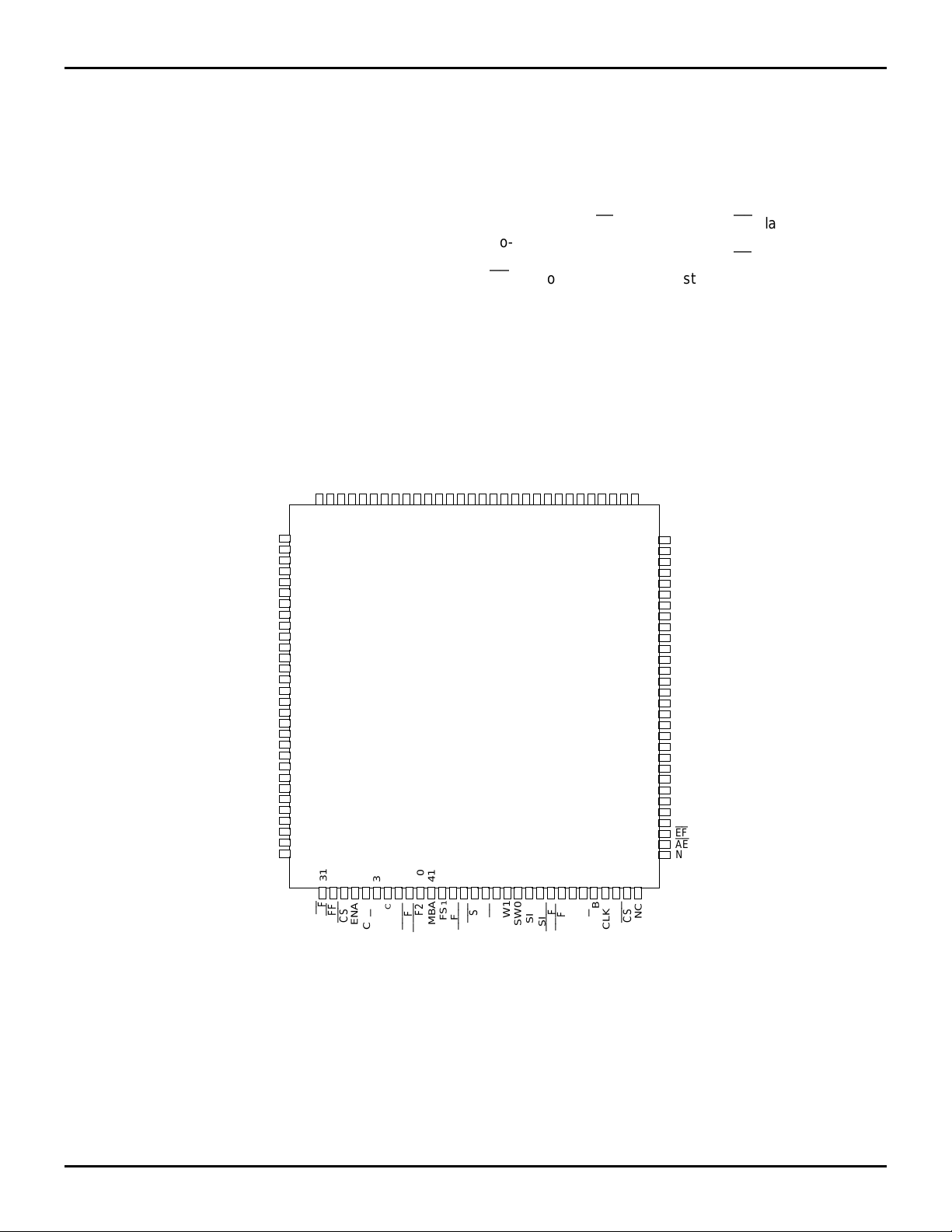
PIN CONFIGURATION
A27
A28
116
115
CLKA
A
R
W/
A29
114
CC
V
30
GND
A
112
113
PGA
A31
111
40
39
PEFA
MBF2
A34
A32
A33
110
109
108
41424344454647
1
FS
MBA
A23
A22
A21
GND
A
A19
A18
A17
A16
A15
A14
A13
A12
A11
A10
GND
A
A8
A7
VCC
A6
A5
A4
A3
GND
A
A1
A0
NC
NC
A24
A25
A26
VCC
120
119
118
117
1
2
3
4
20
5
6
7
8
9
10
11
12
13
14
15
16
9
17
18
19
20
21
22
23
24
25
2
26
27
28
29
30
31
32333435363738
AF
FF
CSA
ENA
through a port are gated to the LOW-to-HIGH transition of a
continuous (free-running) port clock by enable signals. The
continuous clocks for each port are independent of one
another and can be asynchronous or coincident. The enables
for each port are arranged to provide a simple interface
between microprocessors and/or buses with synchronous
interfaces.
The Full Flag (FF) and Almost-Full (AF) flag of the FIFO are
two-stage synchronized to the port clock (CLKA) that writes
data into its array. The Empty Flag (EF) and Almost-Empty
(AE) flag of the FIFO are two-stage synchronized to the port
clock (CLKB) that reads data from its array.
The IDT723613 is characterized for operation from 0°C to
70°C.
23
VCC
B26
B25
B24
B
91
22
B
90
B21
89
GND
88
B
20
87
B19
86
B18
85
B17
84
B16
83
B15
82
B14
81
B13
80
B12
79
B11
78
B10
77
GND
76
B
9
75
B8
74
B7
73
VCC
72
B6
71
B5
70
B4
69
B3
68
GND
67
B
2
66
B1
65
B0
64
EF
63
AE
62
NC
61
60
B
R
NC
CSB
ENB
W/
CLKB
3145 drw 02
FS0
A35
107
EVEN
ODD/
GND
B35
106
105
RST
34
B
B33
104
103
4849505152
BE
SW1
GND
B32
102
SW0
B31
101
SIZ1
29
GND
B30
B28
B27
B
98979695949392
99
100
53545556575859
PGB
SIZ0
PEFB
MBF1
CC
V
NOTE:
1. NC = No internal connection
TQFP (PN120-1, order code: PF)
TOP VIEW
2
IDT723613 CMOS CLOCKED FIFO WITH BUS MATCHING AND BYTE SWAPPING
64 x 36 COMMERCIAL TEMPERATURE RANGES
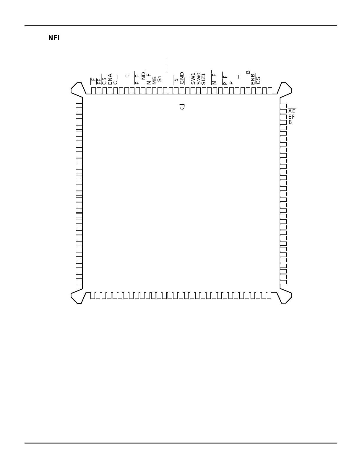
PIN CONFIGURATION (CONTINUED)
GND
NC
NC
A
A1
A2
GND
A
A4
A5
A6
VCC
A7
A8
A9
GND
A
10
A11
VCC
A12
A13
A14
GND
A
15
A16
A17
A18
A19
A20
GND
A
21
A22
A23
1
MBA
FS
0
FS
EVEN
RST
ODD/
2
GND
BE
1
132
SW1
SW0
131
130
SIZ1
SIZ0
129
128
GND
MBF1
127
126
AFFFCSA
17161514131211
18
CLKA
ENA
A
R
W/
CC
V
PGA
10
GND
PEFA
MBF2
9876543
19
20
0
21
*
22
23
24
3
25
26
27
28
29
30
31
32
33
34
35
36
37
38
39
40
41
42
43
44
45
46
47
48
49
50
PGB
PEFB
125
124
CC
V
123
B
R
W/
122
CLKB
ENB
121
120
CSB
119
NC
118
116
115
114
113
112
111
110
109
108
107
106
105
104
103
102
101
100
NC
117
99
98
97
96
95
94
93
92
91
90
89
88
87
86
85
84
GND
AE
EF
B
0
B1
B2
GND
B
3
B4
B5
B6
VCC
B7
B8
B9
GND
B
10
B11
VCC
B12
B13
B14
GND
B
15
B16
B17
B18
B19
B20
GND
B
21
B22
B23
515253545556575859606162636465666768697071727374757677787980818283
CC
A24A25A26A
V
GND
28
A
29
A
CC
V
A30A31A
32
33A34A35
A
GND
27
* Electrical pin 1 in center of beveled edge. Pin 1 identifier in corner.
(2)
PQFP (PQ132-1, order code: PQF)
TOP VIEW
NOTES:
1. NC = No internal connection.
2. Uses Yamaichi socket IC51-1324-828.
35
B
GND
B34B
33
32B31B30
B
GND
CC
V
B29B28B
27
26B25B24
B
GND
CC
V
3145 drw 03
3

IDT723613 CMOS CLOCKED FIFO WITH BUS MATCHING AND BYTE SWAPPING
64 x 36 COMMERCIAL TEMPERATURE RANGES
PIN DESCRIPTION
Symbol Name I/O Description
A
0-A35 Port A Data I/O 36-bit bidirectional data port for side A.
AE
AF
0-B35 Port B Data I/O 36-bit bidirectional data port for side B
B
BE
CLKA Port A Clock I CLKA is a continuous clock that synchronizes all data transfers through port A
CLKB Port B Clock I CLKB is a continuous clock that synchronizes all data transfers through port B
CSA
CSB
EF
ENA Port A Enable I ENA must be HIGH to enable a LOW-to-HIGH transition of CLKA to read or
ENB Port B Enable I ENB must be HIGH to enable a LOW-to-HIGH transition of CLKB to read or
FF
FS
1, FS0 Flag Offset Selects I The LOW-to-HIGH transition of
MBA Port A Mailbox Select I A high level on MBA chooses a mailbox register for a port A read or write
MBF1
MBF2
Almost-Empty Flag O Programmable almost-empty flag synchronized to CLKB. It is LOW when
Port B Port Bthe number of 36-bit words in the FIFO is less than or equal to the value
in the offset register, X.
Almost-Full Flag O Programmable almost-full flag synchronized to CLKA. It is LOW when the
Port A number of 36-bit empty locations in the FIFO is less than or equal to the value in
the offset register, X.
Big-Endian Select I Selects the bytes on port B used during byte or word FIFO reads. A LOW on
BE
selects the most significant bytes on B0-B35 for use, and a HIGH selects
the least significant bytes.
and can be asynchronous or coincident to CLKB. FF and AF are synchronized
to the LOW-to-HIGH transition of CLKA.
and can be asynchronous or coincident to CLKA. Port-B byte swapping and
data port sizing operations are also synchronous to the LOW-to-HIGH transition of CLKB. EF and AE are synchronized to the LOW-to-HIGH transition of
CLKB.
Port A Chip Select I
CSA
must be LOW to enable a LOW-to-HIGH transition of CLKA to read or
write data on port A. The A0-A35 outputs are in the high-impedance state
when
CSA
is HIGH.
Port B Chip Select I
CSB
must be LOW to enable a LOW-to-HIGH transition of CLKB to read or
write data on port B. The B0-B35 outputs are in the high-impedance state
when
CSB
is HIGH.
Empty Flag O
EF
is synchronized to the LOW-to-HIGH transition of CLKB. When EF is LOW,
Port B the FIFO is empty, and reads from its memory are disabled. Data can be read
from the FIFO to its output register when EF is HIGH. EF is forced LOW when
the device is reset and is set HIGH by the second LOW-to-HIGH transition of
CLKB after data is loaded into empty FIFO memory.
write data on port A.
write data on port B.
Full Flag O
FF
is synchronized to the LOW-to-HIGH transition of CLKA. When FF is LOW,
Port A the FIFO is full, and writes to its memory are disabled. FF is forced LOW when
the device is reset and is set HIGH by the second LOW-to-HIGH transition of
CLKA after reset.
RST
latches the values of FS0 and FS1,
which loads one of four preset values into the almost-full flag and almost-empty
flag offsets.
operation. When the A0-A35 outputs are active, mail2 register data is output.
Mail1 Register Flag O
MBF1
is set LOW by a LOW-to-HIGH transition of CLKA that writes data to
the mail1 register. Writes to the mail1 register are inhibited while
LOW.
MBF1
is set HIGH by a LOW-to-HIGH transition of CLKB when a
port B read is selected and both SIZ1 and SIZ0 are HIGH.
MBF1
MBF1
is set
is set HIGH
when the device is reset.
Mail2 Register Flag O
MBF2
is set LOW by a LOW-to-HIGH transition of CLKB that writes data to
the mail2 register. Writes to the mail2 register are inhibited while
LOW.
MBF2
is set HIGH by a LOW-to-HIGH transition of CLKA when a
port A read is selected and MBA is HIGH.
MBF2
is set HIGH when the device
MBF2
is set
is reset.
4

IDT723613 CMOS CLOCKED FIFO WITH BUS MATCHING AND BYTE SWAPPING
64 x 36 COMMERCIAL TEMPERATURE RANGES
PIN DESCRIPTION (CONTINUED)
Symbol Name I/O Description
ODD/ Odd/Even Parity I Odd parity is checked on each port when ODD/
EVEN
Select parity is checked when ODD/
EVEN
is LOW. ODD/
type of parity generated for each port if parity generation is enabled for a read
operation.
PEFA
Port A Parity Error O When any byte applied to terminals A0-A35 fails parity,
Flag (Port A) are organized as A0-A8, A9-A17, A18-A26, and A27-A35, with the most
significant bit of each byte serving as the parity bit. The type of parity
checked is determined by the state of the ODD/
The parity trees used to check the A0-A35 inputs are shared by the mail2
register to generate parity if parity generation is selected by PGA. Therefore, if
a mail2 read with parity generation is set up by having
W/RA LOW, MBA HIGH and PGA HIGH, the
regardless of the state of the A0-A35 inputs.
PEFB
Port B Parity Error O When any valid byte applied to terminals B0-B35 fails parity,
Flag (Port B) Bytes are organized as B0-B8, B9-B17, B-18-B26, and B27-B35, with the
most significant bit of each byte serving as the parity bit. A byte is valid when
it is used by the bus size selected for port B. The type of parity checked is
determined by the state of the ODD/
EVEN
The parity trees used to check the B0-B35 inputs are shared by the mail1
register to generate parity if parity generation is selected by PGB. Therefore, if
a mail1 read with parity generation is set up by having
W/RB LOW, SIZ1 and SIZ0 HIGH and PGB HIGH, the
HIGH regardless of the state of the B0-B35 inputs.
PGA Port A Parity I Parity is generated for data reads from the mail2 register when PGA is HIGH.
Generation The type of parity generated is selected by the state of the ODD/
Bytes are organized at A0-A8, A9-A17, A18-A26, and A27-A35. The generated parity bits are output in the most significant bit of each byte.
PGB Port B Parity I Parity is generated for data reads from port B when PGB is HIGH. The type of
parity generated is selected by the state of the ODD/
organized as B0-B8, B9-B17, B18-B26, and B27-B35. The generated parity
bits are output in the most significant bit of each byte.
RST
Reset I To reset the device, four LOW-to-HIGH transitions of CLKA and four LOW-to-
HIGH transitions of CLKB must occur while
MBF1
, and
MBF2
flags HIGH and the EF, AE, and FF flags LOW. The LOW-
to-HIGH transition of
RST
latches the status of the FS1 and FS0 inputs to
select almost-full flag and almost-empty flag offset.
SIZ0, Port B Bus Size I A LOW-to-HIGH transition of CLKB latches the states of SIZ0, SIZ1, and BE,
SIZ1 Selects (Port B) and the following LOW-to-HIGH transition of CLKB implements the latched
states as a port B bus size. Port B bus sizes can be long word, word, or byte.
A HIGH on both SIZ0 and SIZ1 accesses the mailbox registers for a port B 36-bit
write or read.
SW0, Port B Byte Swap I At the beginning of each long word FIFO read, one of four modes of byte-
SW1 Selects (Port B) order swapping is selected by SW0 and SW1. The four modes are no swap,
byte swap, word swap, and byte-word swap. Byte-order swapping is possible
with any bus-size selection.
W/RA Port A Write/Read I A HIGH selects a write operation and a LOW selects a read operation on
Select port A for a LOW-to-HIGH transition of CLKA. The A0-A35 outputs are in the
high-impedance state when W/RA is HIGH.
W/RB Port B Write/Read I A HIGH selects a write operation and a LOW selects a read operation on
Select port B for a LOW-to-HIGH transition of CLKB. The B0-B35 outputs are in the
high-impedance state when W/RB is HIGH.
EVEN
is HIGH, and even
EVEN
also selects the
PEFA
EVEN
input.
CSA
LOW, ENA HIGH,
PEFA
flag is forced HIGH
input.
CSB
LOW, ENB HIGH,
PEFB
EVEN
input. Bytes are
RST
is LOW. This sets the AF,
is LOW. Bytes
PEFB
is LOW.
flag is forced
EVEN
input.
5

IDT723613 CMOS CLOCKED FIFO WITH BUS MATCHING AND BYTE SWAPPING
64 x 36 COMMERCIAL TEMPERATURE RANGES
ABSOLUTE MAXIMUM RATINGS OVER OPERATING FREE-AIR TEMPERATURE RANGE
(UNLESS OTHERWISE NOTED)
Symbol Rating Commercial Unit
CC Supply Voltage Range -0.5 to 7 V
V
(2)
V
I
O
V
IK Input Clamp Current, (VI < 0 or VI > VCC) ±20 mA
I
I
OK Output Clamp Current, (VO < 0 or VO > VCC) ±50 mA
OUT Continuous Output Current, (VO = 0 to VCC) ±50 mA
I
I
CC Continuous Current Through VCC or GND ±500 mA
A Operating Free-Air Temperature Range 0 to 70 °C
T
STG Storage Temperature Range -65 to 150 °C
T
NOTES:
1. Stresses beyond those listed under "Absolute Maximum Ratings" may cause permanent damage to the device. These are stress ratings only and
functional operation of the device at these or any other conditions beyond those indicated under "Recommended Operating Conditions" is not
implied. Exposure to absolute-maximum-rated conditions for extended periods may affect device reliability.
2. The input and output voltage ratings may be exceeded provided the input and output current ratings are observed.
Input Voltage Range -0.5 to VCC+0.5 V
(2)
Output Voltage Range -0.5 to VCC+0.5 V
(1)
RECOMMENDED OPERATING CONDITIONS
Symbol Parameter Min. Max. Unit
CC Supply Voltage 4.5 5.5 V
V
V
IH High-Level Input Voltage 2 V
IL Low-Level Input Voltage 0.8 V
V
I
OH High-Level Output Current -4 mA
OL Low-Level Output Current 8 mA
I
A Operating Free-Air 0 70 °C
T
Temperature
ELECTRICAL CHARACTERISTICS OVER RECOMMENDED OPERATING FREE-AIR TEMPERATURE RANGE (UNLESS OTHERWISE NOTED)
Parameter Test Conditions Min. Typ.
V
OH VCC = 4.5V, IOH = -4 mA 2.4 V
OL VCC = 4.5 V, IOL = 8 mA 0.5 V
V
I VCC = 5.5 V, VI = VCC or 0 ±50 µA
I
I
OZ VCC = 5.5 V, VO = VCC or 0 ±50 µA
CC VCC = 5.5 V, IO = 0 mA, VI = VCC or GND 1 mA
I
C
i VI = 0, f = 1 MHz 4 pF
o VO = 0, f = 1 MHz 8 pF
C
(1)
Max. Unit
NOTE:
1. All typical values are at VCC = 5 V, TA = 25°C.
6
IDT723613 CMOS CLOCKED FIFO WITH BUS MATCHING AND BYTE SWAPPING
64 x 36 COMMERCIAL TEMPERATURE RANGES
AC ELECTRICAL CHARACTERISTICS OVER RECOMMENDED RANGES OF SUPPLY VOLTAGE
AND OPERATING FREE-AIR TEMPERATURE (SEE FIGURE 4 THROUGH 18)
IDT723613L15 IDT723613L20 IDT723613L30
Symbol Parameter Min. Max. Min. Max. Min. Max. Unit
f
S Clock Frequency, CLKA or CLKB – 66.7 – 50 – 33.4 MHz
CLK Clock Cycle Time, CLKA or CLKB 15 – 20 – 30 – ns
t
CLKH Pulse Duration, CLKA and CLKB HIGH 6–8–12–ns
t
t
CLKL Pulse Duration, CLKA and CLKB LOW 6–8–12–ns
DS Setup Time, A0-A35 before CLKA↑ and B0-B35 4–5–6–ns
t
before CLKB↑
t
ENS Setup Time,
CLKA↑;
SZS Setup Time, SIZ0, SIZ1,and
t
SWS Setup Time, SW0 and SW1 before CLKB↑ 5–7–8–ns
t
t
PGS Setup Time, ODD/
CLKB↑
tRSTS Setup Time,
or CLKB↑
tFSS Setup Time, FS0 and FS1 before
DH Hold Time, A0-A35 after CLKA↑ and B0-B35 1–1–1–ns
t
after CLKB↑
t
ENH Hold Time,
CLKA↑;
SZH Hold Time, SIZ0, SIZ1, and
t
SWH Hold Time, SW0 and SW1 after CLKB↑ 0–0–0–ns
t
t
PGH Hold Time, ODD/
RSTH Hold Time,
t
t
FSH Hold Time, FS0 and FS1 after
(3)
SKEW1
t
Skew Time, between CLKA↑ and CLKB↑ 8–8–10–ns
for EF and
(3)
SKEW2
t
Skew Time, between CLKA↑ and CLKB↑ 9–16–20–ns
for
AE
CSA
, W/RA, ENA, and MBA before 5–5–6–ns
CSB
,W/RB, and ENB before CLKB↑
BE
EVEN
(1)
RST
(2)
CSA
CSB, W/R
LOW before CLKA↑ 5–6–7–ns
W/RA, ENA and MBA after 1–1–1–ns
and PGB before 4–5–6–
B, and ENB after CLKB↑
BE
EVEN
and PGB after CLKB↑
RST
LOW after CLKA↑ or CLKB↑
FF
and
AF
before CLKB↑ 4–5–6–ns
RST
HIGH 5–6–7–ns
after CLKB↑ 2–2–2–ns
(1)
0–0–0–ns
(2)
RST
HIGH 4–4–4–ns
5–6–7–ns
NOTES:
1. Only applies for a clock edge that does a FIFO read.
2. Requirement to count the clock edge as one of at least four needed to reset a FIFO.
3. Skew time is not a timing constraint for proper device operation and is only included to illustrate the timing relationship between CLKA cycle and CLKB
cycle.
7

IDT723613 CMOS CLOCKED FIFO WITH BUS MATCHING AND BYTE SWAPPING
64 x 36 COMMERCIAL TEMPERATURE RANGES
SWITCHING CHARACTERISTICS OVER RECOMMENDED RANGES OF SUPPLY VOLTAGE
AND OPERATING FREE-AIR TEMPERATURE, C
Symbol Parameter Min. Max. Min. Max. Min. Max. Unit
t
A Access Time, CLKA↑ to A0-A35 and CLKB↑ 210212215ns
to B0-B35
t
WFF Propagation Delay Time, CLKA↑ to
REF Propagation Delay Time, CLKB ↑ to
t
PAE Propagation Delay Time, CLKB ↑ to
t
t
PAF Propagation Delay Time, CLKA↑ to
PMF Propagation Delay Time, CLKA↑ to
t
or
MBF2
HIGH and CLKB↑ to
MBF1
HIGH
t
PMR Propagation Delay Time, CLKA↑ to B0-B35
and CLKB↑ to A0-A35
(3)
tPPE
MDV Propagation Delay Time, SIZ1, SIZ0 to 1 11 1 11.5 1 12 ns
t
Propagation delay time, CLKB↑ to
(2)
B0-B35 valid
t
PDPE Propagation Delay Time, A0-A35 valid to
valid; B0-B35 valid to
POPE Propagation Delay Time, ODD/
t
and
PEFB
(4)
t
POPB
Propagation Delay Time, ODD/
PEFB
valid
bits (A8, A17, A26, A35) and (B8, B17, B26,
B35)
PEPE Propagation Delay Time,
t
t
PEPB
MBA, or PGA to
SIZ0, or PGB to
(4)
Propagation Delay Time,
PEFA; CSB
PEFB
CSA
, ENB, W/RB, SIZ1,
CSA
MBA, or PGA to parity bits (A8, A17, A26, A35);
CSB
, ENB, W/RB, SIZ1, SIZ0, or PGB to parity
bits (B8, B17, B26, B35)
RSF Propagation Delay Time,
t
LOW and AF,
t
EN Enable Time,
active and
MBF1, MBF2
CSA
and W/RA LOW to A0-A35 2 10 2 12 2 14 ns
CSB
LOW and W/RB HIGH to
RST
HIGH
B0-B35 active
DIS Disable Time,
t
at high impedance and
CSA
or W/RA HIGH to A0-A35 1 8 1 9 1 11 ns
CSB
HIGH or W/RB
LOW to B0-B35 at high impedance
FF
EF
AE
AF
MBF1
LOW 1 9 1 12 1 15 ns
MBF2
LOW or
PEFB
PEFA
EVEN
to
PEFA
EVEN
to parity 2 12 2 13 2 15 ns
, ENA, W/RA, 111112114ns
, ENA, W/RA, 312313314ns
to AE,
EF
L = 30pF (SEE FIGURE 4 THROUGH 18)
IDT723613L15 IDT723613L20 IDT723613L30
210212215ns
210212215ns
210212215ns
210212215ns
(1)
311312315ns
211212213ns
310311313ns
311312314ns
115120125ns
NOTES:
1. Writing data to the mail1 register when the B0-B35 outputs are active and SIZ1 and SIZ0 are HIGH.
2. Writing data to the mail2 register when the A0-A35 outputs are active.
3. Only applies when a new port-B bus size is implemented by the rising CLKB edge.
4. Only applies when reading data from a mail register.
8
IDT723613 CMOS CLOCKED FIFO WITH BUS MATCHING AND BYTE SWAPPING
64 x 36 COMMERCIAL TEMPERATURE RANGES
FUNCTIONAL DESCRIPTION
RESET (RST)
The IDT723613 is reset by taking the reset (
LOW for at least four port A clock (CLKA) and four port B clock
(CLKB) LOW-to-HIGH transitions. The reset input can switch
asynchronously to the clocks. A device reset initializes the
internal read and write pointers of the FIFO and forces the fullflag (FF) LOW, the empty flag (EF) LOW, the almost-empty
flag (AE) LOW, and the almost-full flag (AF) HIGH. A reset also
forces the mailbox flags (
FF
is set HIGH after two LOW-to-HIGH transitions of CLKA.
MBF1, MBF2
) HIGH. After a reset,
The device must be reset after power up before data is written
to its memory.
A LOW-to-HIGH transition on the
RST
almost-full and almost-empty offset register (X) with the value
selected by the flag select (FS0, FS1) inputs. The values that
can be loaded into the register are shown in Table 1.
TABLE 1: FLAG PROGRAMMING
ALMOST-FULL AND
FS1 FS0
RST
ALMOST-EMPTY FLAG
OFFSET REGISTER (X)
HH↑ 16
HL↑ 12
LH↑ 8
LL↑ 4
RST
) input
input loads the
FIFO WRITE/READ OPERATION
The state of the port A data (A0-A35) outputs is controlled
by the port-A chip select (
CSA
) and the port-A write/read
select (W/RA). The A0-A35 outputs are in the high-impedance
state when either
are active when both
CSA
or W/RA is HIGH. The A0-A35 outputs
CSA
and W/RA are LOW.
Data is loaded into the FIFO from the A0-A35 inputs on
a LOW-to-HIGH transition of CLKA when
is HIGH, ENA is HIGH, MBA is LOW, and
CSA
is LOW, W/RA
FFA
is HIGH (see
Table 2).
The state of the port B data (B0-B35) outputs is controlled by the port B chip select (
CSB
) and the port B write/read
select (W/RB). The B0-B35 outputs are in the high-impedance
state when either
are active when both
CSB
or W/RB is HIGH. The B0-B35 outputs
CSB
and W/RB are LOW. Data is read
from the FIFO to the B0-B35 outputs by a LOW-to-HIGH
transition of CLKB when
HIGH,
EFB
is HIGH, and either SIZ0 or SIZ1 is LOW (see
CSB
is LOW, W/RB is LOW, ENB is
Table 3).
The setup and hold-time constraints to the port clocks for
the port chip selects (
R
A, W/RB) are only for enabling write and read operations and
CSA, CSB
) and write/read selects (W/
are not related to high-impedance control of the data outputs.
If a port enable is LOW during a clock cycle, the port’s chip
select and write/read select can change states during the
setup and hold time window of the cycle.
SYNCHRONIZED FIFO FLAGS
Each FIFO flag is synchronized to its port clock through
two flip-flop stages. This is done to improve the flags’
reliability by reducing the probability of metastable events on
their outputs when CLKA and CLKB operate asynchronously
to one another. FF and AF are synchronized to CLKA. EF and
AE
are synchronized to CLKB. Table 4 shows the relationship
of each port flag to the level of FIFO fill.
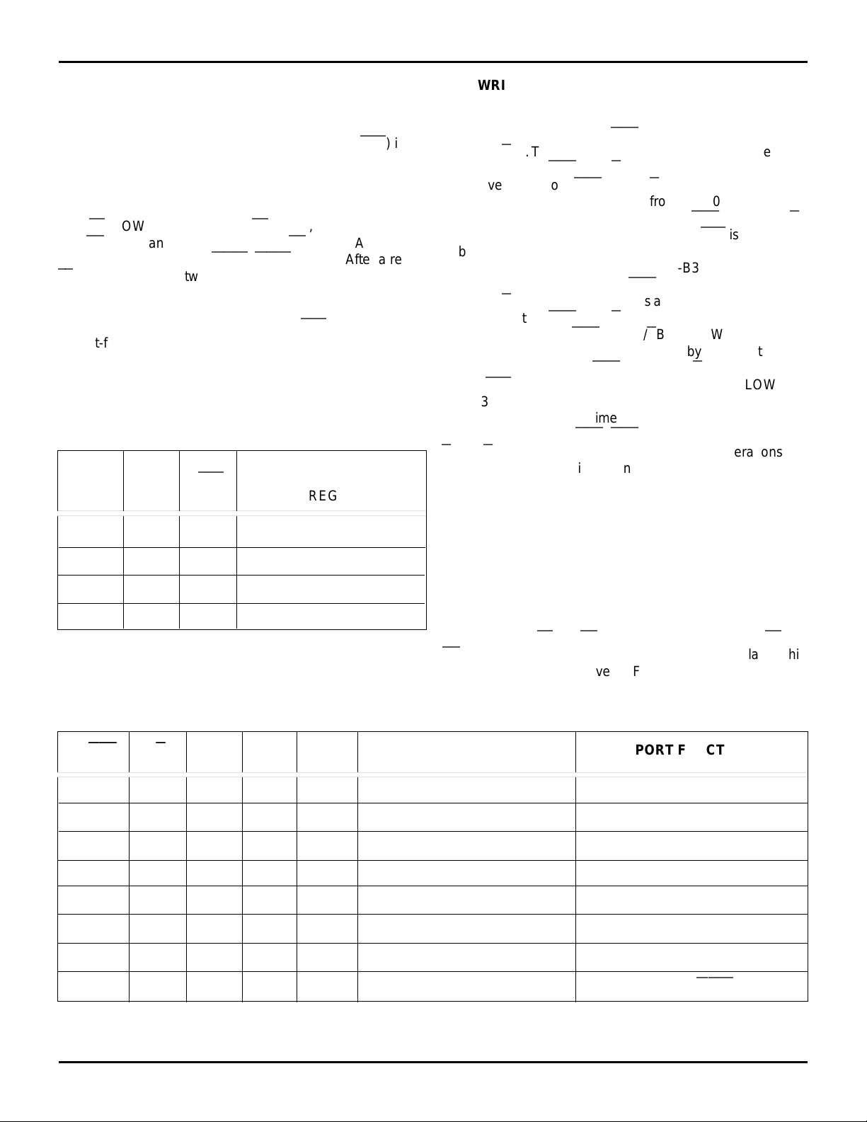
TABLE 2: PORT A ENABLE FUNCTION TABLE
CSA
CSA
W/
RRA ENA MBA CLKA A0-A35 OUPTUTS PORT FUNCTION
H X X X X In high-impedance state None
L H L X X In high-impedance state None
LHH L↑ In high-impedance state FIFO write
LHH H↑ In high impedence state Mail1 write
L L L L X Active, mail2 register None
LLH L↑ Active, mail2 register None
L L L H X Active, mail2 register None
LLHH↑ Active, mail2 register Mail2 read (set
MBF2
HIGH)
9
 Loading...