

Integrated Device Technology Inc IDT7216L16C, IDT7216L16F, IDT7216L16G, IDT7216L16J, IDT7216L20C Datasheet
...
Integrated Device Technology, Inc.
MILITARY AND COMMERCIAL TEMPERATURE RANGES AUGUST 1995
1995 Integrated Device Technology, Inc. 11.3 DSC-2023/6
IDT7216L
IDT7217L
16 x 16 PARALLEL
CMOS MULTIPLIERS
FEATURES:
• 16 x 16 parallel multiplier with double precision product
• 16ns clocked multiply time
• Low power consumption: 120mA
• Produced with advanced submicron CMOS high performance technology
• IDT7216L is pin- and function compatible with TRW
MPY016H/K and AMD Am29516
• IDT7217L requires a single clock with register enables
making it pin- and function compatible with AMD
Am29517
• Configured for easy array expansion
• User-controlled option for transparent output register
mode
• Round control for rounding the MSP
• Input and output directly TTL-compatible
• Three-state output
• Available in Top Braze, DIP, PLCC, Flatpack and Pin
Grid Array
• Military product compliant to MIL-STD-883, Class B
• Standard Military Drawing #5962-86873 is listed on this
function for IDT7216 and Standard Military Drawing
#5962-87686 is listed for this function for IDT7217.
• Speeds available: Commercial: L16/20/25/35/45/55/65
Military: L20/25/30/40/55/65/75
DESCRIPTION:
The IDT7216/IDT7217 are high-speed, low-power
16 x 16-bit multipliers ideal for fast, real time digital signal
processing applications. Utilization of a modified Booths
algorithm and IDT’s high-performance, submicron CMOS
technology, has achieved speeds comparable to bipolar (20ns
max.), at 1/10 the power consumption.
The IDT7216/IDT7217 are ideal for applications requiring
high-speed multiplication such as fast Fourier transform
analysis, digital filtering, graphic display systems, speech
synthesis and recognition and in any system requirement
where multiplication speeds of a mini/microcomputer are
inadequate.
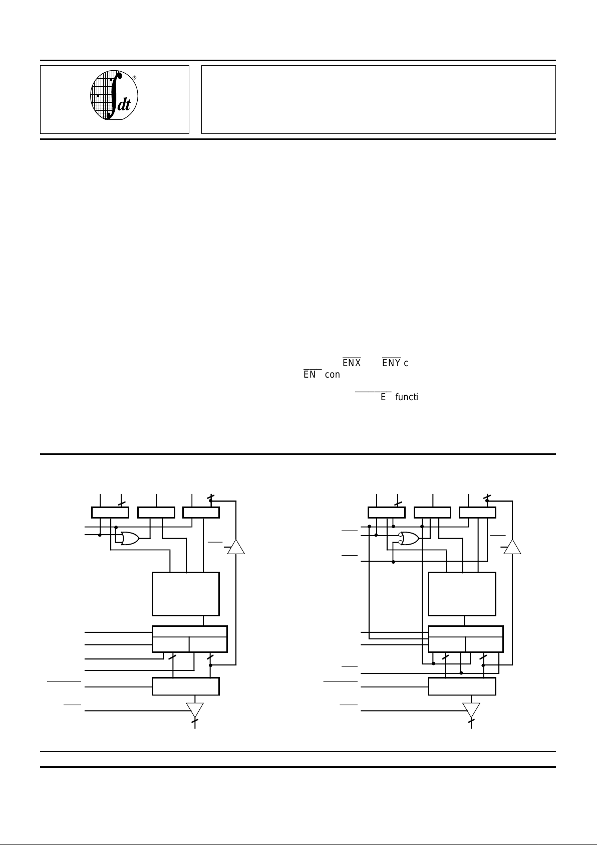
All input registers, as well as LSP and MSP output registers, use the same positive edge-triggered D-type flip-flop. In
the IDT7216, there are independent clocks (CLKX, CLKY,
CLKM, CLKL) associated with each of these registers. The
IDT7217 has only a single clock input (CLK) and three register
enables.
ENX
and
ENY
control the two input registers, while
ENP
controls the entire product.
The IDT7216/IDT7217 offer additional flexibility with the FA
control and
MSPSEL
functions. The FA control formats the
output for two’s complement by shifting the MSP up one bit
and then repeating the sign bit in the MSB of the LSP. The
The IDT Logo is a registered trademark of Integrated Device Technology, Inc.
FUNCTIONAL BLOCK DIAGRAMS
1
2580 drw 01
XREGISTER REGISTER YREGISTER
MULTIPLIER
ARRAY
FORMAT ADJUST
REGISTER
MSP
REGISTER
LSP
MULTIPLEXER
PRODUCT
OEP
MSPSEL
CLKL
CLKM
FT
FA
OEL
CLKX
CLKY
X
M X15-0 RND YM Y15-0/P15-0
16
16
16 16
16
XREGISTER REGISTER YREGISTER
MULTIPLIER
ARRAY
FORMAT ADJUST
REGISTER
MSP
REGISTER
LSP
MULTIPLEXER
PRODUCT
OEP
MSPSEL
ENP
FT
FA
OEL
ENX
CLK
X
M X15-0 RND YM Y15-0/P15-0
16
16
16 16
16
MSPOUT (P31 - P16) MSPOUT (P31 - P16)
2580 drw 02
ENY
IDT7216
IDT7217

11.3 2
IDT7216L, IDT7217L
16 x 16 PARALLEL CMOS MULTIPLIERS MILITARY AND COMMERCIAL TEMPERATURE RANGES
DESCRIPTION (Cont’d.)
The IDT7216/IDT7217 multipliers are manufactured in
compliance with the latest revision of MIL-STD-883, Class B,
making them ideally suited to applications demanding the
highest level of performance and reliability.
MSPSEL
low selects the MSP to be available at the product
output port, while a high selects the LSP to be available.
Keeping this pin low will ensure compatibility with the TRW
MPY016H.
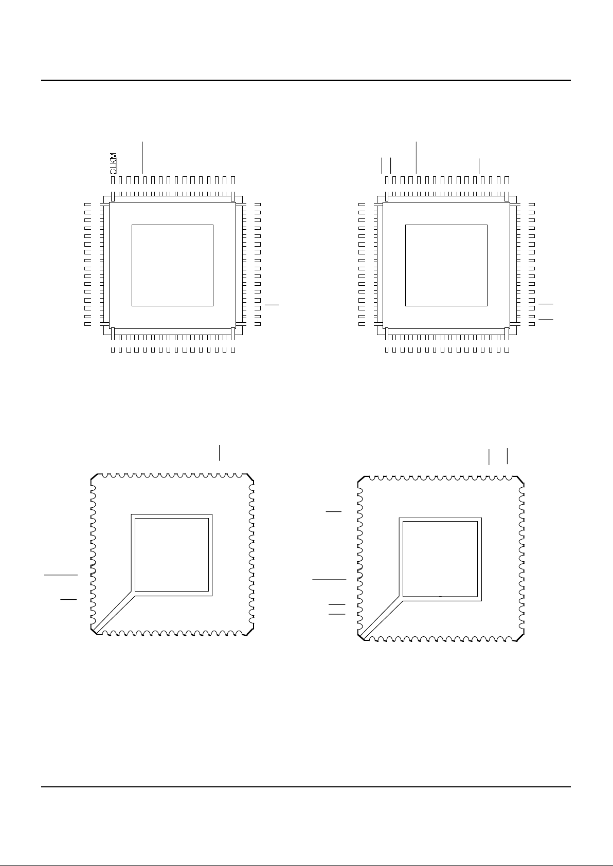
PIN CONFIGURATIONS
IDT7216 IDT7217
64-PIN DIP
TOP VIEW
64-PIN DIP
TOP VIEW
C64-2
2580 drw 03
X4
X3
X2
X1
X0
OEL
CLKL
CLKY
P
7, P23
P6, P22
P5, P21
P4, P20
P3, P19
P2, P18
P0, P16
P1, P17
P15, Y15
P14, Y14
P13, Y13
P12, Y12
P11, Y11
P9, Y9
P10, Y10
P8, Y8
P7, Y7
P6, Y6
P5, Y5
P4, Y4
P3, Y3
P2, Y2
P1, Y1
P0, Y0
1
2
3
4
5
6
7
8
9
10
11
12
13
14
15
16
17
18
19
20
21
22
23
24
25
26
27
28
29
30
31
32
64
63
62
61
60
59
58
57
56
55
54
53
52
51
50
49
48
47
46
45
44
43
42
41
40
39
38
37
36
35
34
33
X
5
X6
X7
X8
X9
X10
X11
X12
P8, P24
P9, P25
P10, P26
P11, P27
P12, P28
P13, P29
P15, P31
P14, P30
CLKM
OEP
FA
FT
MSPSEL
GND
GND
V
CC
VCC
YM
XM
RND
CLKX
X
15
X14
X13
C64-2
2580 drw 04
X4
X3
X2
X1
X0
OEL
CLK
ENY
P
7, P23
P6, P22
P5, P21
P4, P20
P3, P19
P2, P18
P0, P16
P1, P17
P15, Y15
P14, Y14
P13, Y13
P12, Y12
P11, Y11
P9, Y9
P10, Y10
P8, Y8
P7, Y7
P6, Y6
P5, Y5
P4, Y4
P3, Y3
P2, Y2
P1, Y1
P0, Y0
1
2
3
4
5
6
7
8
9
10
11
12
13
14
15
16
17
18
19
20
21
22
23
24
25
26
27
28
29
30
31
32
64
63
62
61
60
59
58
57
56
55
54
53
52
51
50
49
48
47
46
45
44
43
42
41
40
39
38
37
36
35
34
33
X
5
X6
X7
X8
X9
X10
X11
X12
P8, P24
P9, P25
P10, P26
P11, P27
P12, P28
P13, P29
P15, P31
P14, P30
ENP
OEP
FA
FT
MSPSEL
GND
GND
V
CC
VCC
YM
XM
RND
ENX
X
15
X14
X13

11.3 3
IDT7216L, IDT7217L
16 x 16 PARALLEL CMOS MULTIPLIERS MILITARY AND COMMERCIAL TEMPERATURE RANGES
PIN CONFIGURATIONS (Cont’d.)
NC X13 X15 RND YM VCC GND FT OEP
X
12 X14
ENX*
XM VCC GND
MSP-
SEL
FA NCX11
X9 X10
P30,
P14
X7 X8
X5 X6
X3 X4
X1 X2
OEL X0
NC
NC
11
10
09
08
07
06
05
04
03
02
01
ABCDEFGHJKL
Pin 1
Designator
G68-2
2580 drw 05
CLKX
or
ENP*
CLKM
or
CLKY
or
ENY*
CLKL
or
CLK*
P31,
P15
P28,
P12
P29,
P13
P26,
P10
P27,
P11
P24,P8P25,
P9
P22,P6P23,
P7
P20,P4P21,
P5
P18,P2P19,
P3
P16,P0P17,
P1
Y0,P0Y2,P2Y4,P4Y6,P6Y8,P8Y10,
P10
Y12,
P12
Y14,
P14
Y1,P1Y3,P3Y5,P5Y7,P7Y9,P9Y11,
P11
Y13,
P13
Y15,
P15
*Pin designation for IDT7217
IDT7216/IDT7217
PGA
TOP VIEW
11.3 4
IDT7216L, IDT7217L
16 x 16 PARALLEL CMOS MULTIPLIERS MILITARY AND COMMERCIAL TEMPERATURE RANGES
32
CLK
NC
X
12
X11
X10
X9X8X7X6X5
X4X3X2X1X0
OEL
10111213141516 17181920 212223 2425 26
605958 57565554 535251504948 4746 45 44
61
62
63
64
65
66
67
68
1
2
3
4
5
6
7
8
9
43
42
41
40
39
38
37
36
35
34
33
31
30
29
28
27
X13
X14
X15
ENX
RND
X
M
YM
VCC
VCC
GND
GND
MSPSEL
FT
FA
OEP
ENP
NC
NC
NC
2580 drw 09
ENY
P12, P28
P11, P27
P10, P26
P9, P25
P8, P24
P7, P23
P6, P22
P5, P21
P4, P20
P3, P19
P2, P18
P1, P17
P13, P29
P14, P30
P15, P31
P15, Y15
P14, Y14
P13, Y13
P12, Y12
P11, Y11
P10, Y10
P9, Y9
P8, Y8
P7, Y7
P6, Y6
P5, Y5
P4, Y4
P3, Y3
P2, Y2
P1, Y1
P0, Y0
L68-1, L68-1
P0, P16
ENP
48
47
46
45
44
43
42
41
40
39
38
37
36
35
34
33
17181920212223242526 272829 303132
64636261605958575655 545352 515049
1
2
3
4
5
6
7
8
9
10
11
12
13
14
15
16
P15, P31
P14, P30
P13, P29
P12, P28
P11, P27
P10, P26
P9, P25
P8, P24
P7, P23
P6, P22
P5, P21
P4, P20
P3, P19
P2, P18
P1, P17
P0, P16
X12
X11
X10
X9
X8
X7
X6
X5
X4
X3
X2
X1
X0
OEL
CLK
ENY
P15, Y15
P14, Y14
P13, Y13
P12, Y12
P11, Y11
P10, Y10
P9, Y9
P8, Y8
P7, Y7
P6, Y6
P5, Y5
P4, Y4
P3, Y3
P2, Y2
P1, Y1
P0, Y0
OEPFAFT
MSPSEL
GND
GND
VCCVCCYMXM
RND
ENX
X
15
X13
X14
2580 drw 07
F64-1
PIN CONFIGURATIONS (Cont’d.)
IDT7216 IDT7217
64-LEAD FLATPACK
TOP VIEW
64-LEAD FLATPACK
TOP VIEW
PLCC
TOP VIEW
PLCC
TOP VIEW
IDT7216 IDT7217
2
3
5
6
NC
X
12
X11
X10X9X8X7X6X5X4X3X2X1X0
OEL
L68-1, L68-1
60 59 58 57565554 53 5251 50 4948 47 46 45 44
61
62
63
64
65
66
67
68
1
43
42
41
40
39
38
37
36
35
34
33
32
31
30
29
28
27
X
13
X
14
X
15
CLKX
RND
X
M
Y
M
V
CC
V
CC
GND
GND
MSPSEL
FT
FA
OEP
CLKM
9
NC
NC
NC
2580 drw 08
CLKY
P12, P28
P11, P27
P10, P26
P9, P25
P8, P24
P7, P23
P6, P22
P5, P21
P4, P20
P3, P19
P2, P18
P1, P17
P13, P29
P14, P30
P15, P31
P15, Y
15
P14, Y
14
P13, Y
13
P12, Y
12
P11, Y
11
P10, Y
10
P9, Y
9
P8, Y
8
P7, Y
7
P6, Y
6
P5, Y
5
P4, Y
4
P3, Y
3
P2, Y
2
P1, Y
1
P0, Y
0
101112 13 14 1516 171819 20 212223 24 25 26
4
7
8
P0, P16
CLKL
J68-1
J68-1
48
47
46
45
44
43
42
41
40
39
38
37
36
35
34
33
17181920 212223242526 272829303132
64636261 605958575655 545352515049
1
2
3
4
5
6
7
8
9
10
11
12
13
14
15
16
X12
X11
X10
X9
X8
X7
X6
X5
X4
X3
X2
X1
X0
OEL
CLKL
P15, Y15
P14, Y14
P13, Y13
P12, Y12
P11, Y11
P10, Y10
P9, Y9
P8, Y8
P7, Y7
P6, Y6
P5, Y5
P4, Y4
P3, Y3
P2, Y2
P1, Y1
P0, Y0
OEP
FA
FT
MSPSE
L
GND
GND
VCCVCCYMXM
RND
CLKX
X
15
X13
X14
2580 drw 06
F64-1
P15, P31
P14, P30
P13, P29
P12, P28
P11, P27
P10, P26
P9, P25
P8, P24
P7, P23
P6, P22
P5, P21
P4, P20
P3, P19
P2, P18
P1, P17
P0, P16 CLKY
 Loading...