

IDT IDT7200L, IDT7201LA, IDT7202LA User Manual
Integrated Device Technology, Inc.
W
CMOS ASYNCHRONOUS FIFO
256 x 9, 512 x 9, 1K x 9
IDT7200L
IDT7201LA
IDT7202LA
FEATURES:
• First-In/First-Out dual-port memory
• 256 x 9 organization (IDT7200)
• 512 x 9 organization (IDT7201)
• 1K x 9 organization (IDT7202)
• Low power consumption
— Active: 770mW (max.)
—Power-down: 2.75mW (max.)
• Ultra high speed—12ns access time
• Asynchronous and simultaneous read and write
• Fully expandable by both word depth and/or bit width
• Pin and functionally compatible with 720X family
• Status Flags: Empty, Half-Full, Full
• Auto-retransmit capability
• High-performance CEMOS technology
• Military product compliant to MIL-STD-883, Class B
• Standard Military Drawing #5962-87531, 5962-89666,
5962-89863 and 5962-89536 are listed on this function
• Industrial temperature range (-40oC to +85oC) is
available, tested to military electrical specifications
DESCRIPTION:
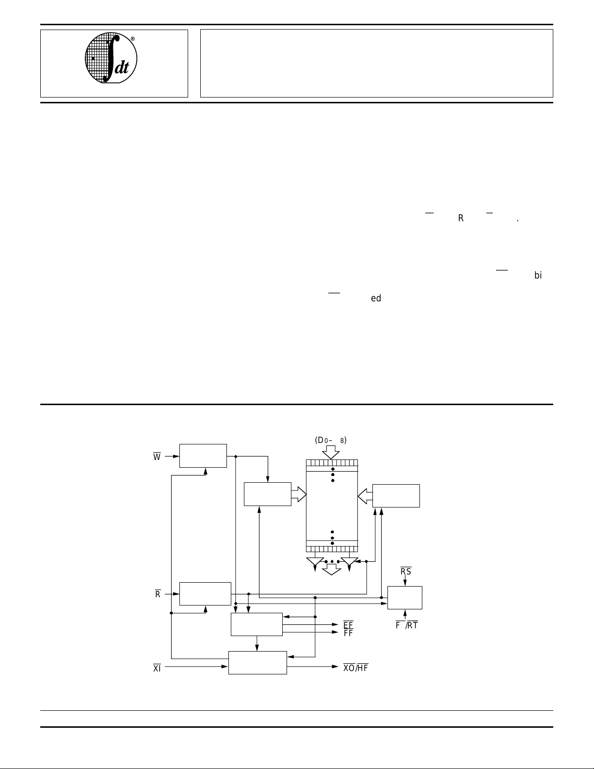
The IDT7200/7201/7202 are dual-port memories that load
and empty data on a first-in/first-out basis. The devices use
Full and Empty flags to prevent data overflow and underflow
and expansion logic to allow for unlimited expansion capability
in both word size and depth.
The reads and writes are internally sequential through the
use of ring pointers, with no address information required to
load and unload data. Data is toggled in and out of the devices
through the use of the Write (W) and Read (R) pins.
The devices utilizes a 9-bit wide data array to allow for
control and parity bits at the user’s option. This feature is
especially useful in data communications applications where
it is necessary to use a parity bit for transmission/reception
error checking. It also features a Retransmit (RT) capability
that allows for reset of the read pointer to its initial position
when RT is pulsed low to allow for retransmission from the
beginning of data. A Half-Full Flag is available in the single
device mode and width expansion modes.
The IDT7200/7201/7202 are fabricated using IDT’s highspeed CMOS technology. They are designed for those
applications requiring asynchronous and simultaneous read/
writes in multiprocessing and rate buffer applications. Military
grade product is manufactured in compliance with the latest
revision of MIL-STD-883, Class B.
FUNCTIONAL BLOCK DIAGRAM
DATA INPUTS
0(D –D8)
WRITE
CONTROL
WRITE
POINTER
R
XI
The IDT logo is a trademark of Integrated Device Technology, Inc.
READ
CONTROL
EXPANSION
THREESTATE
BUFFERS
FLAG
LOGIC
LOGIC
MILITARY AND COMMERCIAL TEMPERATURE RANGES DECEMBER 1996
1996 Integrated Device Technology, Inc. DSC-2679/7
For latest information contact IDT's web site at www.idt.com or fax-on-demand at 408-492-8391.
5.03 1
RAM
ARRAY
256 x 9
512 x 9
1024 x 9
DATA OUTPUTS
0(Q –Q8)
EF
FF
XO/HF
READ
POINTER
RS
RESET
LOGIC
FL/RT
2679 drw 01
IDT7200/7201A/7202A CMOS ASYNCHRONOUS FIFO
256 x 9, 512 x 9 and 1K x 9 MILITARY AND COMMERCIAL TEMPERATURE RANGES
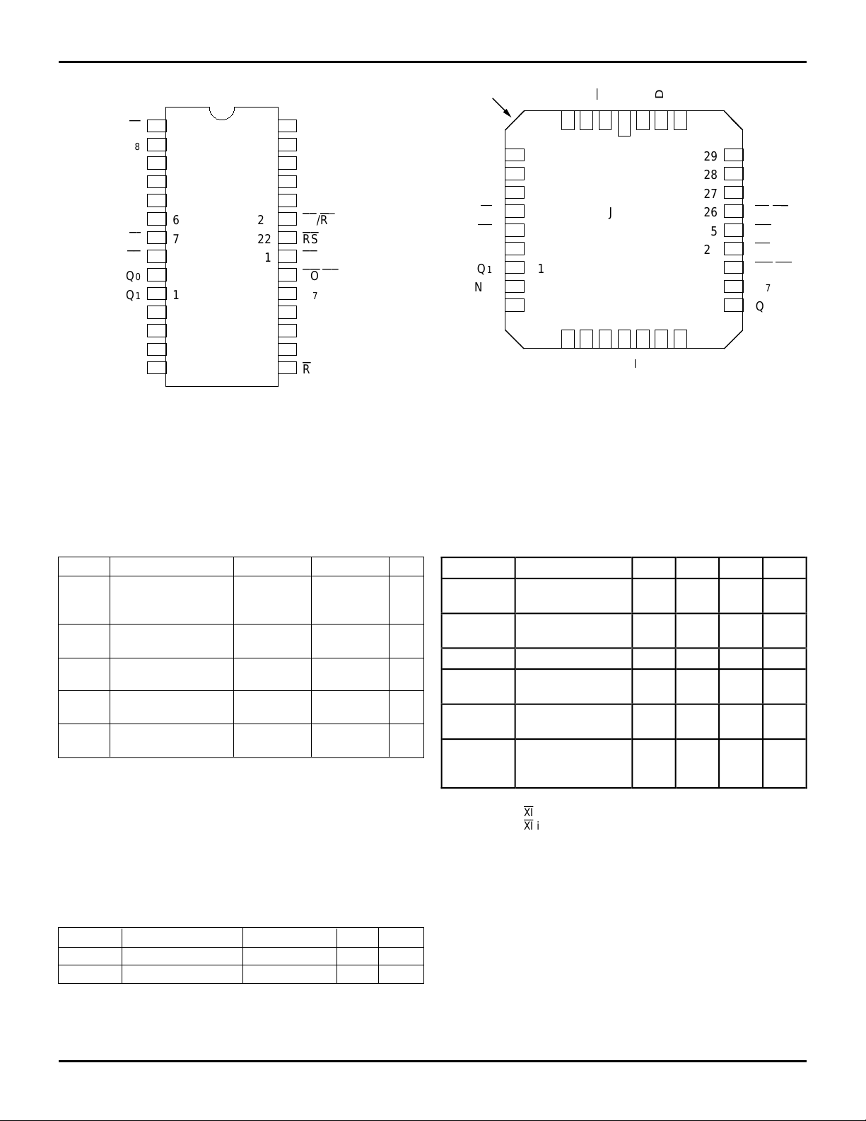
PIN CONFIGURATIONS
W
D8
1
2
28
27
D3 D5326
D2 D6425
D1 D7524
D0
XI RS
FF EF
Q0
P28-1,
P28-2,
623
D28-1,
D28-3,
722
E28-2,
821
SO28-3
920
Q1 Q710 19
Q2 Q611 18
Q3 Q512 17
Q8 Q413 16
GND
14 15
DIP/SOIC/CERPACK
TOP VIEW
NOTE:
1. CERPACK (E28-2) and 600-mil-wide DIP (P28-1 and D28-1) not available
for 7200.
VCC
D4
FL/RT
XO/HF
R
2679 drw 02a
INDEX
D
2
D
1
D
0
XI
FF
Q
0
Q
1
5
6
7
8
9
10
11
D8
D3
W
4
3 2132 31 30
J32-1
L32-1
NC 12
Q
2
13
14 15 16 17 18 19 20
Q3
Q8
GND
LCC/PLCC
TOP VIEW
NOTE:
1. LCC (L32-1) not available for 7200.
CC
D4
NC
&
NC
D5
V
D
29
28
27
26
25
24
23
22
21
4
R
Q5
Q
6
D
7
NC
FL/RT
RS
EF
XO/HF
Q
7
Q
6
2679 drw 02b
ABSOLUTE MAXIMUM RATINGS
(1)
Symbol Rating Com’l. Mil. Unit
V
TERM Terminal Voltage –0.5 to +7.0 –0.5 to +7.0 V
with Respect
to GND
T
A Operating 0 to +70 –55 to +125 °C
Temperature
T
BIAS Temperature –55 to +125 –65 to +135 °C
Under Bias
T
STG Storage –55 to +125 –65 to +155 °C
Temperature
I
OUT DC Output 50 50 mA
Current
NOTE: 2679 tbl 01
1. Stresses greater than those listed under ABSOLUTE MAXIMUM RATINGS
may cause permanent damage to the device. This is a stress rating only
and functional operation of the device at these or any other conditions
above those indicated in the operational sections of this specification is not
implied. Exposure to absolute maximum rating conditions for extended
periods may affect reliabilty.
CAPACITANCE (TA = +25°C, f = 1.0 MHz)
Symbol Parameter
IN Input Capacitance VIN = 0V 8 pF
C
OUT Output Capacitance VOUT = 0V 8 pF
C
NOTE: 2679 tbl 02
1. This parameter is sampled and not 100% tested.
(1)
Condition Max. Unit
RECOMMENDED DC OPERATING
CONDITIONS
Symbol Parameter Min. Typ. Max. Unit
V
CCM
V
CCC
GND Supply Voltage 0 0 0 V
(1)
V
IH
(1)
V
IH
(2)
V
IL
NOTE: 2679 tbl 03
1. VIH = 2.6V for XI input (commercial).
IH = 2.8V for
V
2. 1.5V undershoots are allowed for 10ns once per cycle.
Military Supply
Voltage
Commercial Supply
Voltage
Input High Voltage
Commercial
Input High Voltage
Mlitary
Input Low Voltage
Commercial and
Military
XI
input (military).
4.5 5.0 5.5 V
4.5 5.0 5.5 V
2.0 — — V
2.2 — — V
— — 0.8 V
5.03 2
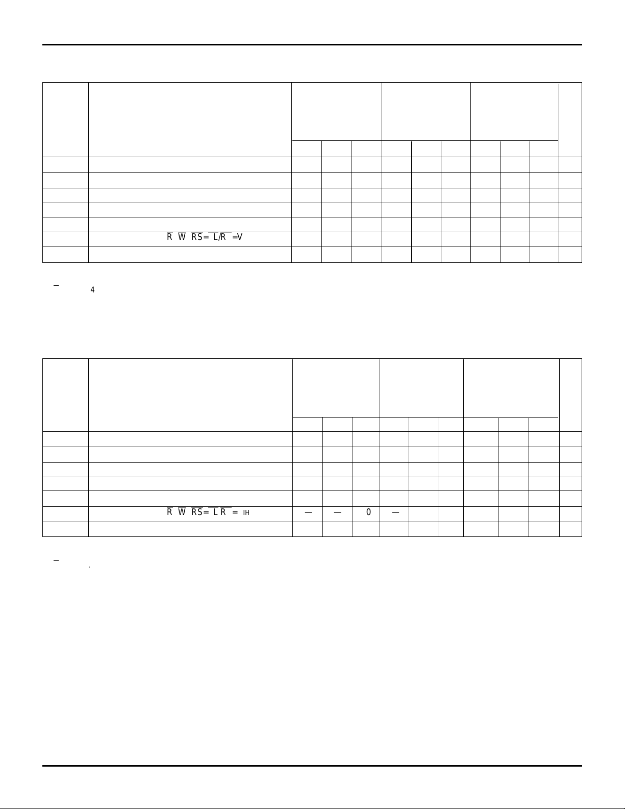
IDT7200/7201A/7202A CMOS ASYNCHRONOUS FIFO
256 x 9, 512 x 9 and 1K x 9 MILITARY AND COMMERCIAL TEMPERATURE RANGES
DC ELECTRICAL CHARACTERISTICS
(Commercial: VCC = 5.0V±10%, TA = 0°C to +70°C; Military: VCC = 5.0V±10%, TA = –55°C to +125°C)
IDT7200L IDT7200L IDT7200L
IDT7201LA IDT7201LA IDT7201LA
IDT7202LA IDT7202LA IDT7202LA
Commercial Military Commercial
t
A = 12, 15, 20 ns tA = 20 ns tA = 25, 35 ns
Symbol Parameter Min. Typ. Max. Min. Typ. Max. Min. Typ. Max. Unit
(1)
LI
I
(2)
LO
I
OH Output Logic “1” Voltage IOH = –2mA 2.4 — — 2.4 — — 2.4 — — V
V
OL Output Logic “0” Voltage IOL = 8mA — — 0.4 — — 0.4 — — 0.4 V
V
(3)
CC1
I
(3)
CC2
I
CC3(L)
I
Input Leakage Current (Any Input) –1 — 1 –10 — 10 –1 — 1 µA
Output Leakage Current –10 — 10 –10 — 10 –10 — 10 µA
Active Power Supply Current — — 125
(4)
— — 140
(4)
— — 125
(4)
mA
Standby Current (R=W=RS=FL/RT=VIH)——15——20——15mA
(3)
Power Down Current (All Input = VCC - 0.2V) — — 0.5 — — 0.9 — — 0.5 mA
NOTES: 2679 tbl 05
1. Measurements with 0.4 ≤ VIN ≤ VCC.
2.R ≥ V
3. I
4. Tested at f = 20MHz.
IH, 0.4 ≤ VOUT ≤ VCC.
CC measurements are made with outputs open (only capacitive loading).
2679 tbl 04
DC ELECTRICAL CHARACTERISTICS (Continued)
(Commercial: VCC = 5.0V±10%, TA = 0°C to +70°C; Military: VCC = 5.0V±10%, TA = –55°C to +125°C)
IDT7200L IDT7200L IDT7200L
IDT7201LA IDT7201LA IDT7201LA
IDT7202LA IDT7202LA IDT7202LA
Military Commercial Military
t
A = 30, 40 ns tA = 50 ns tA = 50, 65, 80, 120 ns
Symbol Parameter Min. Typ. Max. Min. Typ. Max. Min. Typ. Max. Unit
(1)
LI
I
(2)
LO
I
OH Output Logic “1” Voltage IOH = –2mA 2.4 — — 2.4 — — 2.4 — — V
V
OL Output Logic “0” Voltage IOL = 8mA — — 0.4 — — 0.4 — — 0.4 V
V
(3)
CC1
I
(3)
CC2
I
CC3(L)
I
NOTES: 2679 tbl 05
1. Measurements with 0.4 ≤ VIN ≤ VCC.
2.R ≥ V
3. I
CC measurements are made with outputs open (only capacitive loading).
4. Tested at f = 20MHz.
Input Leakage Current (Any Input) –10 — 10 –1 — 1 –10 — 10 µA
Output Leakage Current –10 — 10 –10 — 10 –10 — 10 µA
Active Power Supply Current — — 140
(4)
— 50 80 — 70 100 mA
Standby Current (R=W=RS=FL/RT=VIH)——20—58—815mA
(3)
Power Down Current (All Input = VCC - 0.2V) — — 0.9 — — 0.5 — — 0.9 mA
IH, 0.4 ≤ VOUT ≤ VCC.
5.03 3
IDT7200/7201A/7202A CMOS ASYNCHRONOUS FIFO
256 x 9, 512 x 9 and 1K x 9 MILITARY AND COMMERCIAL TEMPERATURE RANGES
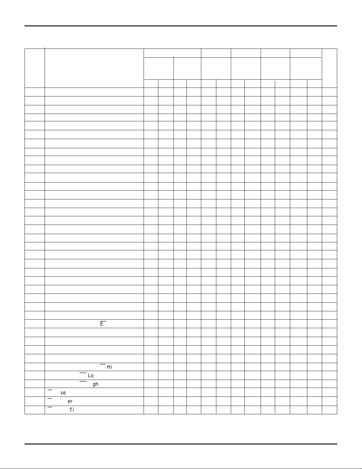
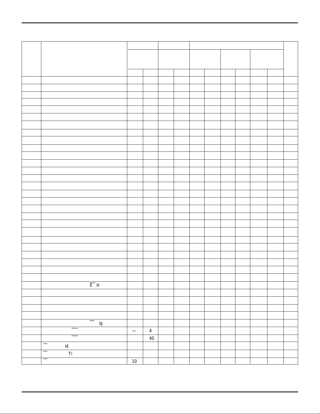
AC ELECTRICAL CHARACTERISTICS
(1)
(Commercial: VCC = 5.0V±10%, TA = 0°C to +70°C; Military: VCC = 5.0V±10%, TA = –55°C to +125°C)
Commercial Com'l & Mil. Com'l Military Com'l
7200L12 7200L15 7200L20 7200L25 7200L30 7200L35
7201LA12 7201LA15 7201LA20 7201LA25 7201LA30 7201LA35
7202LA12 7202LA15 7202LA20 7202LA25 7202LA30 7202LA35
Symbol Parameter Min. Max. Min. Max. Min. Max. Min. Max. Min. Max. Min. Max. Unit
S Shift Frequency — 50 — 40 — 33.3 — 28.5 — 25 — 22.2 MHz
t
RC Read Cycle Time 20 — 25 — 30 — 35 — 40 — 45 — ns
t
A Access Time — 12 — 15 — 20 — 25 — 30 — 35 ns
t
RR Read Recovery Time 8 — 10 — 10 — 10 — 10 — 10 — ns
t
RPW Read Pulse Width
t
RLZ Read Pulse Low to Data Bus at Low Z
t
WLZ Write Pulse High to Data Bus at Low Z
t
DV Data Valid from Read Pulse High 5 — 5 — 5 — 5 — 5 — 5 — ns
t
RHZ Read Pulse High to Data Bus at High Z
t
WC Write Cycle Time 20 — 25 — 30 — 35 — 40 — 45 — ns
t
WPW Write Pulse Width
t
WR Write Recovery Time 8 — 10 — 10 — 10 — 10 — 10 — ns
t
DS Data Set-up Time 9 — 11 — 12 — 15 — 18 — 18 — ns
t
DH Data Hold Time 0 — 0 — 0 — 0 — 0 — 0 — ns
t
RSC Reset Cycle Time 20 — 25 — 30 — 35 — 40 — 45 — ns
t
RS Reset Pulse Width
t
RSS Reset Set-up Time
t
RSR Reset Recovery Time 8 — 10 — 10 — 10 — 10 — 10 — ns
t
RTC Retransmit Cycle Time 20 — 25 — 30 — 35 — 40 — 45 — ns
t
RT Retransmit Pulse Width
t
RTS Retransmit Set-up Time
t
RTR Retransmit Recovery Time 8 — 10 — 10 — 10 — 10 — 10 — ns
t
EFL Reset to Empty Flag Low — 12 — 25 — 30 — 35 — 40 — 45 ns
t
HFH,FFH Reset to Half-Full and Full Flag High — 17 — 25 — 30 — 35 — 40 — 45 ns
t
RTF Retransmit Low to Flags Valid — 20 — 25 — 30 — 35 — 40 — 45 ns
t
REF Read Low to Empty Flag Low — 12 — 15 — 20 — 25 — 30 — 30 ns
t
RFF Read High to Full Flag High — 14 — 15 — 20 — 25 — 30 — 30 ns
t
RPE Read Pulse Width after
t
WEF Write High to Empty Flag High — 12 — 15 — 20 — 25 — 30 — 30 ns
t
WFF Write Low to Full Flag Low — 14 — 15 — 20 — 25 — 30 — 30 ns
t
WHF Write Low to Half-Full Flag Low — 17 — 25 — 30 — 35 — 40 — 45 ns
t
RHF Read High to Half-Full Flag High — 17 — 25 — 30 — 35 — 40 — 45 ns
t
WPF Write Pulse Width after
t
XOL Read/Write to
t
XOH Read/Write to
t
XI
t
XIR
t
XIS
t
NOTES: 2679 tbl 06
1. Timings referenced as in AC Test Conditions. 3. Values guaranteed by design, not currently tested.
2. Pulse widths less than minimum value are not allowed. 4. Only applies to read data flow-through mode.
XI
Pulse Width
XI
Recovery Time 8 — 10 — 10 — 10 — 10 — 10 — ns
XI
Set-up Time 8 — 10 — 10 — 10 — 10 — 10 — ns
(2)
(2)
(2)
(3)
(2)
(3)
EF
High 12 — 15 — 20 — 25 — 30 — 35 — ns
FF
High 12 — 15 — 20 — 25 — 30 — 35 — ns
XO
Low — 12 — 15 — 20 — 25 — 30 — 35 ns
XO
High — 12 — 15 — 20 — 25 — 30 — 35 ns
(2)
12 — 15 — 20 — 25 — 30 — 35 — ns
(3)
3—5—5—5— 5 —5—ns
(3, 4)
3—5—5—5— 5 —10—ns
(3)
— 12 — 15 — 15 — 18 — 20 — 20 ns
12 — 15 — 20 — 25 — 30 — 35 — ns
12 — 15 — 20 — 25 — 30 — 35 — ns
12 — 15 — 20 — 25 — 30 — 35 — ns
12 — 15 — 20 — 25 — 30 — 35 — ns
12 — 15 — 20 — 25 — 30 — 35 — ns
12 — 15 — 20 — 25 — 30 — 35 — ns
5.03 4
IDT7200/7201A/7202A CMOS ASYNCHRONOUS FIFO
256 x 9, 512 x 9 and 1K x 9 MILITARY AND COMMERCIAL TEMPERATURE RANGES
AC ELECTRICAL CHARACTERISTICS
(1)
(Continued)
(Commercial: VCC = 5.0V±10%, TA = 0°C to +70°C; Military: VCC = 5.0V±10%, TA = –55°C to +125°C)
Military Com'l & Mil. Military
7200 L40 7200L50 7200L65 7200L80 7200L120
7201LA40 7201LA50 7201LA65 7201LA80 7201LA120
7202LA40 7202LA50 7202LA65 7202LA80 7202LA120
Symbol Parameter Min. Max. Min. Max. Min. Max. Min. Max. Min. Max. Unit
t
S Shift Frequency — 20 — 15 — 12.5 — 10 — 7 MHz
RC Read Cycle Time 50 — 65 — 80 — 100 — 140 — ns
t
A Access Time — 40 — 50 — 65 — 80 — 120 ns
t
RR Read Recovery Time 10 — 15 — 15 — 20 — 20 — ns
t
RPW Read Pulse Width
t
RLZ Read Pulse Low to Data Bus at Low Z
t
WLZ Write Pulse High to Data Bus at Low Z
t
DV Data Valid from Read Pulse High 5 — 5 — 5 — 5 — 5 — ns
t
RHZ Read Pulse High to Data Bus at High Z
t
WC Write Cycle Time 50 — 65 — 80 — 100 — 140 — ns
t
WPW Write Pulse Width
t
WR Write Recovery Time 10 — 15 — 15 — 20 — 20 — ns
t
DS Data Set-up Time 20 — 30 — 30 — 40 — 40 — ns
t
DH Data Hold Time 0 — 5 — 10 — 10 — 10 — ns
t
RSC Reset Cycle Time 50 — 65 — 80 — 100 — 140 — ns
t
RS Reset Pulse Width
t
RSS Reset Set-up Time
t
RSR Reset Recovery Time 10 — 15 — 15 — 20 — 20 — ns
t
RTC Retransmit Cycle Time 50 — 65 — 80 — 100 — 140 — ns
t
RT Retransmit Pulse Width
t
RTS Retransmit Set-up Time
t
RTR Retransmit Recovery Time 10 — 15 — 15 — 20 — 20 — ns
t
EFL Reset to Empty Flag Low — 50 — 65 — 80 — 100 — 140 ns
t
HFH,FFH Reset to Half-Full and Full Flag High — 50 — 65 — 80 — 100 — 140 ns
t
RTF Retransmit Low to Flags Valid — 50 — 65 — 80 — 100 — 140 ns
t
REF Read Low to Empty Flag Low — 30 — 45 — 60 — 60 — 60 ns
t
RFF Read High to Full Flag High — 35 — 45 — 60 — 60 — 60 ns
t
RPE Read Pulse Width after
t
WEF Write High to Empty Flag High — 35 — 45 — 60 — 60 — 60 ns
t
WFF Write Low to Full Flag Low — 35 — 45 — 60 — 60 — 60 ns
t
WHF Write Low to Half-Full Flag Low — 50 — 65 — 80 — 100 — 140 ns
t
RHF Read High to Half-Full Flag High — 50 — 65 — 80 — 100 — 140 ns
t
WPF Write Pulse Width after
t
XOL Read/Write to
t
XOH Read/Write to
t
XI
t
XIR
t
XIS
t
NOTES: 2679 tbl 07
1. Timings referenced as in AC Test Conditions 4. Values guaranteed by design, not currently tested.
2. Speed grades 65, 80 and 120 not available in the CERPACK 5. Only applies to read data flow-through mode.
3. Pulse widths less than minimum value are not allowed.
XI
Pulse Width
XI
Recovery Time 10 — 10 — 10 — 10 — 10 — ns
XI
Set-up Time 10 — 15 — 15 — 15 — 15 — ns
(3)
(3)
(3)
(4)
(3)
(4)
EF
High 40 — 50 — 65 — 80 — 120 — ns
FF
High 40 — 50 — 65 — 80 — 120 — ns
XO
Low — 40 — 50 — 65 — 80 — 120 ns
XO
High — 40 — 50 — 65 — 80 — 120 ns
(3)
40 — 50 — 65 — 80 — 120 — ns
(4)
5 — 10 — 10 — 10 — 10 — ns
(4, 5)
10 — 15 — 15 — 20 — 20 — ns
(4)
— 25 — 30 — 30 — 30 — 35 ns
40 — 50 — 65 — 80 — 120 — ns
40 — 50 — 65 — 80 — 120 — ns
40 — 50 — 65 — 80 — 120 — ns
40 — 50 — 65 — 80 — 120 — ns
40 — 50 — 65 — 80 — 120 — ns
40 — 50 — 65 — 80 — 120 — ns
(2)
5.03 5
 Loading...