

IDT IDT71V65802 User Manual
A0-A18Address Inputs
Input
Synchronous
1
, CE2,
2
Chip Enab les
Input
Synchronous
Outp ut E nable
Input
Asynchronous
R/WRe ad/ Wri te Sig n al
Input
Synchronous
Cloc k Enab le
Input
Synchronous
1
,
2
,
3
,
4
Individual Byte Write Selects
Input
Synchronous
CLK
Clock
Input
N/A
ADV/LDAdvance burst address / Load new address
Input
Synchronous
Linear / Interleaved Burst Order
Input
StaticZZSleep Mode
Input
Asynchronous
I/O0-I/O31, I/OP1-I/OP4Data Input / Outp ut
I/O
Synchronous
VDD, V
DD Q
Co re P o we r, I/O Powe r
Supply
Static
VSSGround
Supply
Static
查询IDT71V65602供应商
256K x 36, 512K x 18
3.3V Synchronous ZBT™ SRAMs
2.5V I/O, Burst Counter
Pipelined Outputs
Features
◆◆
◆
◆◆
256K x 36, 512K x 18 memory configurations
◆◆
◆
◆◆
Supports high performance system speed - 150MHz
(3.8ns Clock-to-Data Access)
◆◆
◆
◆◆
ZBTTM Feature - No dead cycles between write and read cycles
◆◆
◆
◆◆
Internally synchronized output buffer enable eliminates the
need to control
◆◆
◆
◆◆
Single R/
◆◆
◆
◆◆
Positive clock-edge triggered address, data, and control
signal registers for fully pipelined applications
◆◆
◆
◆◆
4-word burst capability (interleaved or linear)
◆◆
◆
◆◆
Individual byte write (
◆◆
◆
◆◆
Three chip enables for simple depth expansion
◆◆
◆
◆◆
3.3V power supply (±5%)
◆◆
◆
◆◆
2.5V I/O Supply (VDDQ)
◆◆
◆
◆◆
Power down controlled by ZZ input
◆◆
◆
◆◆
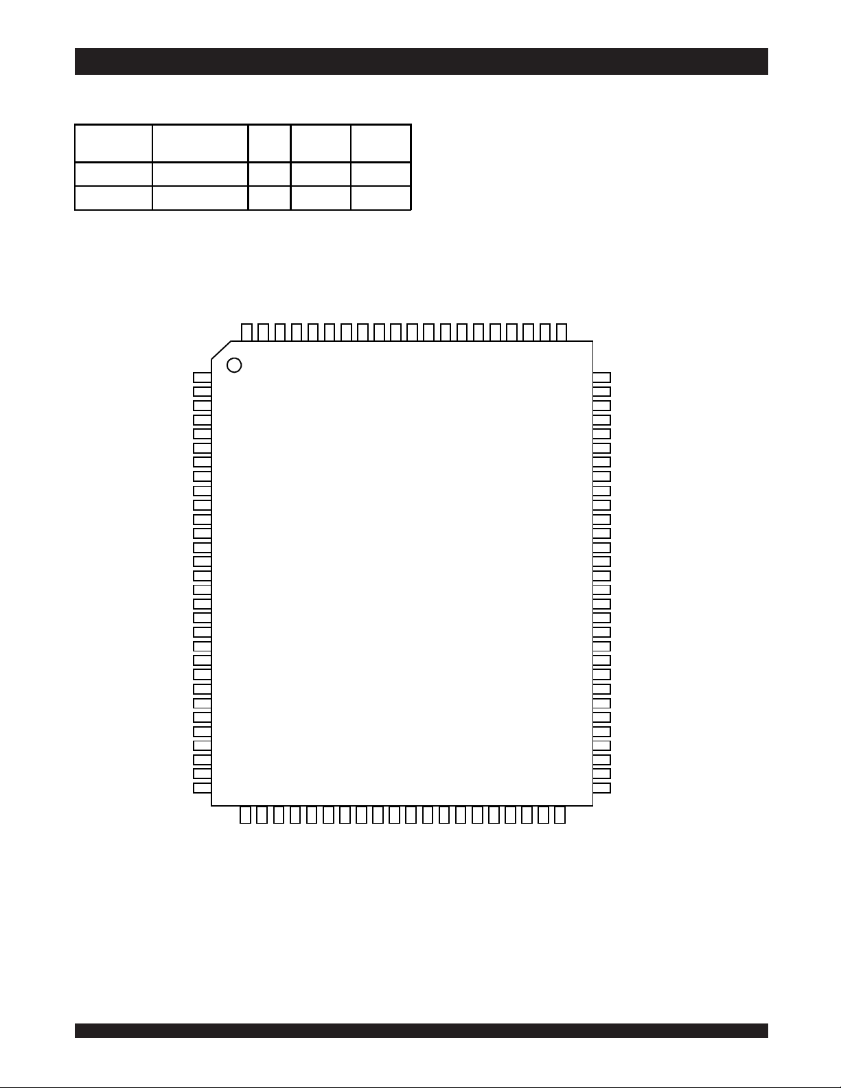
Packaged in a JEDEC standard 100-pin plastic thin quad and
OEOE
OE
OEOE
WW
W (READ/WRITE) control pin
WW
BWBW
BWBW
BW1 -
BW4) control (May tie active)
BWBW
BWBW
flatpack (TQFP), 119 ball grid array (BGA) and 165 fine pitch
ball grid array (fBGA)
Description
The IDT71V65602/5802 are 3.3V high-speed 9,437,184-bit
(9 Megabit) synchronous SRAMs. They are designed to eliminate dead
bus cycles when turning the bus around between reads and writes, or
writes and reads. Thus, they have been given the name ZBTTM, or Zero
Bus Turnaround.
IDT71V65602
IDT71V65802
Address and control signals are applied to the SRAM during one clock
cycle, and two cycles later the associated data cycle occurs, be it read or write.
The IDT71V65602/5802 contain data I/O, address and control signal
registers. Output enable is the only asynchronous signal and can be used to
disable the outputs at any given time.
A Clock Enable (CEN) pin allows operation of the IDT71V65602/5802
to be suspended as long as necessary. All synchronous inputs are ignored
when (CEN) is high and the internal device registers will hold their previous
values.
There are three chip enable pins (CE1, CE2, CE2) that allow the
user to deselect the device when desired. If any one of these three are not
asserted when ADV/LD is low, no new memory operation can be initiated.
However, any pending data transfers (reads or writes) will be completed. The
data bus will tri-state two cycles after chip is deselected or a write is initiated.
The IDT71V65602/5802 have an on-chip burst counter. In the burst
mode, the IDT71V65602/5802 can provide four cycles of data for a single
address presented to the SRAM. The order of the burst sequence is defined
by the LBO input pin. The LBO pin selects between linear and interleaved burst
sequence. The ADV/LD signal is used to load a new external address (ADV/
LD = LOW) or increment the internal burst counter (ADV/LD = HIGH).
The IDT71V65602/5802 SRAM utilize IDT's latest high-performance
CMOS process, and are packaged in a JEDEC Standard 14mm x 20mm 100pin thin plastic quad flatpack (TQFP) as well as a 119 ball grid array (BGA)
and a 165 fine pitch ball grid array (fBGA).
Pin Description Summary
CE
OE
CEN
BW
LBO
ZBT and Zero Bus Turnaround are trademarks of Integrated Device Technology, Inc. and the architecture is supported by Micron Technology and Motorola, Inc.
©2004 Integrated Device Technology, Inc.
BW
CE
BW
BW
1
5303 tbl 01
OCTOBER 2004
DSC-5303/05
IDT71V65602, IDT71V65802, 256K x 36, 512K x 18, 3.3V Synchronous SRAMs with
Symbol
Pin Function
I/O
Active
Description
18
1
4
1
4
1
4
1
2
1
2
1
2
2
1
2
2
1
2
31
P4
DD
DDQ
SS
ZBT
Feature, 2.5V I/O, Burst Counter, and Pipelined Outputs Commercial and Industrial Temperature Ranges
Pin Definitions
(1)
A0-A
ADV/
BW
CE
R/
CEN
-
,
W
BW
CE
LD
Address Inputs I N/A Synchronous Address inputs. The address register is triggered by a combination of the
rising edge of CLK, ADV/
LD
low,
low, and true chip enab le s.
CEN
Advance / Load I N/A ADV/LD is a synchronous input that is used to load the internal registers with new address
and control when it is sampled low at the rising edge of clock with the chip selected. When
ADV/
is low with the chip deselected, any burst in progress is terminated. When ADV/
LD
is s amp l e d hi g h the n the inte r nal b ur st c o unte r i s ad va nc e d fo r any burs t that was in
progress. The external addresses are ignored when ADV/
is sampled high.
LD
Re ad / Write I N/A R/W signal is a synchronous input that identifies whether the current load cycle initiated is a
Read or Write access to the memory array. The data bus activity for the current cycle takes
place two clock cycle s later.
Clock Enable I LOW Synchronous Clock Enable Input. When
inputs, including clock are ignored and outputs re main unchanged. The effect of
is samp led hig h, al l other s y nchrono us
CEN
CEN
sampled high on the device outputs is as if the low to high clock transition did not occur.
Individual Byte
Write E nab le s
For normal operation,
I LOW Synchro nous byte write enables. Each 9-bit byte has its own active low byte write enable.
On load write c yc le s (When R/
signal (
-
) must be valid. The byte write signal must also b e valid on each cycle of
BW
BW
a burst write. Byte Write signals are ignored when R/
b yte (s ) o f d ata ar e writte n i nto the de vi c e two cy c le s l ate r.
must be sampled low at rising edge of clock.
CEN
and ADV/LD are sampled low) the appropriate byte write
W
is sampled high. The appropriate
W
BW
-
can all be tied low if
BW
always doing write to the entire 36-bit word.
Chip E nables I LOW Synchronous active low chip enable.
IDT71V65 602/ 5802 . (
CE
or
sampled high or CE2 sampled low) and ADV/LD low at the
CE
rising edge of clock, initiates a deselect cycle. The ZBT
CE
and
are us e d wi th CE2 to e nab le the
CE
TM
has a two cycle deselect, i.e.,
the data bus will tri-state two clock cycles after deselect is initiated.
LD
CE
CLK Clock I N/A This is the clock input to the IDT71V65602/5802. Except for
Chip Enab le I HIGH Sync hrono us active hig h c hip e nable . CE2 is used with
CE
has inverted polarity but otherwise identical to
CE
and
CE
and
to e nab le the c hip .
CE
.
CE
, all tim ing re fe re n ce s fo r the
OE
device are made with respect to the rising edge of CLK.
I/O0-I/O
I/OP1-I/O
LBO
Data Input/Output I/O N/A Synchro nous data input/output (I/O) pins. Both the data input path and data output path are
registered and triggered by the rising edge of CLK.
Linear Burst Order I LOW Burst order selection input. When
When
is low the Linear burst sequence is selected.
LBO
is high the Interleaved burst sequence is selected.
LBO
is a static input and it must
LBO
not change during device operation.
OE
Outp ut E nab l e I LOW As y nc hro no us o utp ut e na b le . OE must be lo w to read d ata from the IDT71V65602/5802.
When
actively controlled for read and write cycles. In normal operation,
is high the I/O pins are in a high-impedance state. OE does not need to be
OE
can be tied low.
OE
ZZ Sleep Mode I HIGH Asynchronous sleep mode input. ZZ HIGH will gate the CLK internally and power down
71V65602/5802 to the lowest power consumption level. Data retention is guaranteed in
Sleep Mode.
V
V
V
NOTE:
Po we r S up p ly N/ A N/ A 3 .3V c o re p o we r s up p l y.
Power Supply N/A N/A 2.5V I/O Supply.
Ground N/A N/A Ground.
1. All synchronous inputs must meet specified setup and hold times with respect to CLK.
5303 tbl 02
6.422
IDT71V65602, IDT71V65802, 256K x 36, 512K x 18, 3.3V Synchronous SRAMs with
ZBT
Feature, 2.5V I/O, Burst Counter, and Pipelined Outputs Commercial and Industrial Temperature Ranges
Functional Block Diagram
LBO
Address A [0:17]
CE1, CE2, CE2
R/W
CEN
ADV/LD
BWx
Clock
DQ
DQ
egister
Input R
DQ
Clk
Address
Control
Control Logic
Clk
256Kx36 BIT
MEMORY ARRAY
DI DO
Mux
D
Output Register
Q
Sel
OE
Gate
Data I/O[0:31],
I/O P[1:4]
5303 drw 01a
,
6.42
3
IDT71V65602, IDT71V65802, 256K x 36, 512K x 18, 3.3V Synchronous SRAMs with
Symbol
Para mete r
Min.
Typ.
Max.
Unit
ZBT
Feature, 2.5V I/O, Burst Counter, and Pipelined Outputs Commercial and Industrial Temperature Ranges
Functional Block Diagram
Address A [0:18]
CE1, CE2, CE2
ADV/LD
Clock
LBO
R/W
CEN
BWx
DQ
DQ
egister
Input R
DQ
Clk
Address
Control
Control Logic
Clk
512x18 BIT
MEMORYARRAY
DI DO
Mux
D
Output Register
Q
Sel
OE
Recommended DC Operating
Conditions
DD
V
Core S upp ly Vo ltage 3.135 3.3 3.465 V
DDQ
I/O Sup p ly Vol tage 2 .375 2.5 2.625 V
V
SS
Supply Voltage 0 0 0 V
V
IH
Input High Voltage - Inputs 1.7
V
IH
Input High Voltage - I/O 1.7
V
IL
Input Low Voltage -0.3
V
NOTES:
1. V IL (min.) = –1.0V for pulse width less than tCYC/2, once per cycle.
____
VDD+0.3 V
____
DDQ
V
+0.3 V
(1 )
____
0.7 V
5303 tbl 03
6.424
Gate
DataI/O [0:15],
I/O P[1:2]
5303 drw 01
,
IDT71V65602, IDT71V65802, 256K x 36, 512K x 18, 3.3V Synchronous SRAMs with
Grade
Ambient
Temperature
(1)
VSSVDDV
DDQ
ZBT
Feature, 2.5V I/O, Burst Counter, and Pipelined Outputs Commercial and Industrial Temperature Ranges
Recommended Operating
Temperature and Supply Voltage
Comme rcial 0° C to +70° C 0V 3. 3V± 5% 2.5V±5%
Industrial -40° C to +85° C 0V 3.3V±5% 2.5V± 5%
NOTES:
5303tb l 05
1. During production testing, the case temperature equals the ambient temperature.
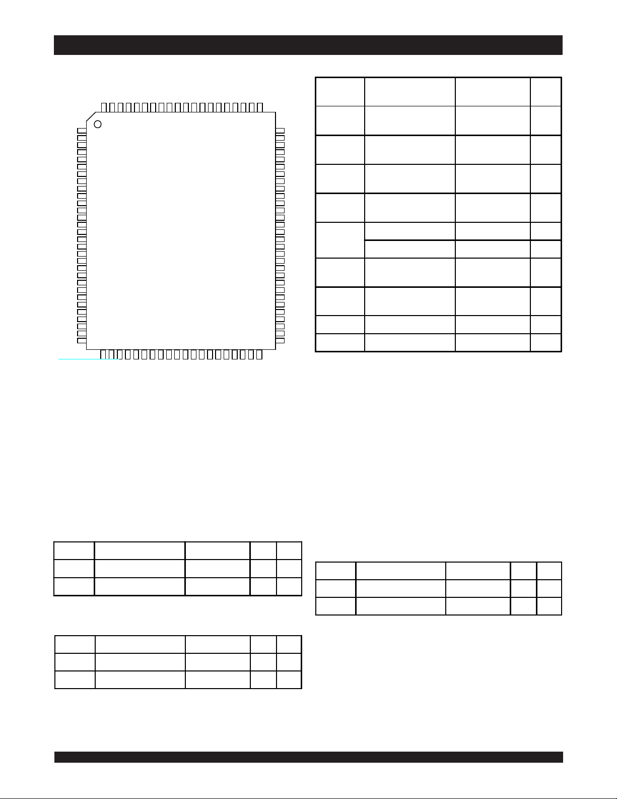
Pin Configuration - 256K x 36
LD
4
3
2
2
1
7
E
W
E
A6A
10099989796959493929190 8786858483828189 88
B
C
C
1
2
D
S
LK
D
W
W
W
B
B
B
S
E
C
C
V
V
W
/
R
/
(2)
V
N
E
C
D
E
A
N
O
C
9
17
A8A
A
V
V
I/O
V
V
V
V
I/O
I/O
I/O
DDQ
V
I/O
I/O
I/O
I/O
V
DDQ
I/O
I/O
DD
V
DD
V
I/O
I/O
DDQ
V
I/O
I/O
I/O
I/O
V
DDQ
I/O
I/O
P3
SS
SS
DD
SS
SS
SS
P4
1
2
16
3
17
4
5
6
18
7
19
8
20
9
21
10
11
12
22
13
23
(1)
14
15
(1)
16
17
18
24
19
25
20
21
22
26
23
27
24
28
25
29
26
27
28
30
29
31
30
31 32 33 34 35 36 37 38 39 40 41 42 43 44 45 46 47 48 49 50
O
LB
5
(3)
(3)
A0A1A2A3A4A
S
S
U
U
V
N
N
D
D
(3)
(3)
D
D
U
U
V
N
N
D
D
14A13A12A11A10
A
A15A
16
80
79
78
77
76
75
74
73
72
71
70
69
68
67
66
65
64
63
62
61
60
59
58
57
56
55
54
53
52
51
I/O
I/O
I/O
DDQ
V
V
SS
I/O
I/O
I/O
I/O
V
SS
V
DDQ
I/O
I/O
V
SS
V
DD
V
DD
ZZ
I/O
I/O
DDQ
V
V
SS
I/O
I/O
I/O
I/O
V
SS
V
DDQ
I/O
I/O
I/O
5303 drw 02
P2
15
14
13
12
11
10
9
8
(1)
7
6
5
4
3
2
1
0
P1
,
Top View
100 TQFP
NOTES:
1. Pins 14, 16 and 66 do not have to be connected directly to VDD as long as the input voltage is ≥ VIH.
2. Pin 84 is reserved for a future 16M.
3. DNU=Do not use. Pins 38, 39, 42 and 43 are reserved for respective JTAG pins: TMS, TDI, TDO and TCK. The
current die revision allows these pins to be left unconnected, tied Low (VSS) or tied High (VDD).
6.42
5
IDT71V65602, IDT71V65802, 256K x 36, 512K x 18, 3.3V Synchronous SRAMs with
Symbol
Rating
Com mercial &
Industrial
Unit
V
TE R M
(2 )
Ter mi nal Vo l tag e wi th
Re s p ec t to G ND
-0.5 to +4.6
V
V
TE R M
(3,6)
Ter mi nal Vo l tag e wi th
Re s p ec t to G ND
-0.5 to V
DD
V
V
TE R M
(4,6)
Ter mi nal Vo l tag e wi th
Re s p ec t to G ND
-0.5 to V
DD
+0.5
V
V
TE R M
(5,6)
Ter mi nal Vo l tag e wi th
Re s p ec t to G ND
-0.5 to V
DDQ
+0.5
V
T
A
(7)
Co mme rci al
-0 to +70
o
C
Indus trial
-40 to +85
o
C
T
BIAS
Temperature
Und e r B i as
-55 to +125
o
C
T
STG
Storage
Temperature
-55 to +125
o
C
PTPo we r Di ss i p ati o n
2.0WI
OUT
DC Outp ut Cu rre n t
50
mA
5303 tbl 06
Symbol
Parameter
(1)
Conditions
Max.
Unit
CINInp ut Cap ac itanc e
VIN = 3dV
5pFC
I/O
I/O Cap acitanc e
V
OUT
= 3dV
7
pF
5303 tbl 07
Symbol
Parameter
(1)
Conditions
Max.
Uni t
IN
I/O
OUT
Symb ol
Par a meter
(1)
Conditions
Max .
Unit
CINInp ut Capa ci tanc e
VIN = 3dV
TBDpFC
I/O
I/O Cap aci tance
V
OUT
= 3dV
TBD
pF
5303 tb l 0 7b
ZBT
Feature, 2.5V I/O, Burst Counter, and Pipelined Outputs Commercial and Industrial Temperature Ranges
Pin Configuration - 512K x 18
LD
2
2
1
7
E
E
A6A
C
C
100 99 98 97 96 95 94 93 92 91 90 87 86 85 84 83 82 8189 88
1
NC
2
NC
3
NC
4
DDQ
V
5
SS
V
6
NC
7
NC
8
8
I/O
9
9
I/O
10
SS
V
11
DDQ
V
12
10
I/O
13
11
I/O
(1)
14
DD
V
15
DD
V
(1)
16
DD
V
17
V
SS
18
I/O
12
19
I/O
13
20
DDQ
V
21
SS
V
22
14
I/O
23
I/O
15
24
I/O
P2
25
NC
26
SS
V
27
DDQ
V
28
NC
29
NC
30
NC
31 32 33 34 35 36 37 38 39 40 41 42 43 44 45 46 47 48 49 50
5
O
LB
1
2
D
S
C
C
W
W
B
B
N
N
(3)
A0A1A2A3A4A
U
N
D
LK
D
S
E
C
V
V
C
(3)
(3)
S
D
S
D
U
U
V
V
N
N
D
D
/
(2)
V
N
W
E
D
C
E
/
C
R
(3)
U
N
D
18
A
N
O
A
15A14A13A12A11
A
A8A
A16A
9
17
80
79
78
77
76
75
74
73
72
71
70
69
68
67
66
65
64
63
62
61
60
59
58
57
56
55
54
53
52
51
5303drw 02a
Absolute Maximum Ratings
A
10
NC
NC
DDQ
V
SS
V
NC
I/O
P1
7
I/O
I/O
6
SS
V
V
DDQ
5
I/O
4
I/O
SS
V
(1)
DD
V
DD
V
ZZ
I/O
3
I/O
2
DDQ
V
SS
V
1
I/O
0
I/O
NC
NC
V
SS
V
DDQ
NC
NC
NC
,
NOTES:
1. Stresses greater than those listed under ABSOLUTE MAXIMUM RATINGS may
(1)
cause permanent damage to the device. This is a stress rating only and functional
Top View
100 TQFP
NOTES:
1. Pins 14, 16 and 66 do not have to be connected directly to VDD as long as
the input voltage is ≥ VIH.
2. Pin 84 is reserved for a future 16M.
3. DNU=Do not use. Pins 38, 39, 42 and 43 are reserved for respective
JTAG pins: TMS, TDI, TDO and TCK. The current die revision allows
these pins to be left unconnected, tied Low (VSS) or tied High (VDD).
operation of the device at these or any other conditions above those indicated
in the operational sections of this specification is not implied. Exposure to absolute
maximum rating conditions for extended periods may affect reliability.
2. VDD terminals only.
3. VDDQ terminals only.
4. Input terminals only.
5. I/O terminals only.
6. This is a steady-state DC parameter that applies after the power supply has
reached its nominal operating value. Power sequencing is not necessary;
however, the voltage on any input or I/O pin cannot exceed VDDQ during power
supply ramp up.
7. During production testing, the case temperature equals TA.
100 TQFP Capacitance
(TA = +25° C, f = 1.0MHz)
(1)
119 BGA Capacitance
(1)
(TA = +25° C, f = 1.0MHz)
165 fBGA Capacitance
(TA = +25° C, f = 1.0MHz)
NOTE:
1. This parameter is guaranteed by device characterization, but not production tested.
(1)
6.426
C
Inp ut Ca p ac itan c e VIN = 3dV 7 pF
I/O Cap a ci tanc e V
C
= 3dV 7 pF
5303 tbl 07a
IDT71V65602, IDT71V65802, 256K x 36, 512K x 18, 3.3V Synchronous SRAMs with
ZBT
Feature, 2.5V I/O, Burst Counter, and Pipelined Outputs Commercial and Industrial Temperature Ranges
Pin Configuration - 256K X 36, 119 BGA
1234567
DDQ
V
A
B NC CE
NC
C A
16
D
E I/O
F V
G
H I/O
J V
K I/O
L I/O
M V
N I/O
P I/O
I/O
DDQ
I/O
DDQ
DDQ
I/O
17
I/O
I/O
20
I/O
22
I/O
24
I/O
25
I/O
I/O
29
I/O
31
I/O
R NC A
T NC NC A
U V
DDQ
DNU
2
6
A
2
7
P3
18
19
21
23
DD
V
26
27
28
30
P4
5
(3)
A
A
A
SS
V
SS
V
SS
V
BW
SS
V
DD(1)
V
SS
V
BW
SS
V
SS
V
SS
V
LBO
10
DNU
4
3
2
NC(2)
ADV/LD
DD
V
NC V
1
CE
OE
A17
3
W
R/
DD
V
CLK V
NC
4
CEN
1
A
0
A
DD
V
11
A
DNU
(3)
(3)
A
A
A
SS
SS
V
SS
V
BW
SS
V
DD(1)
V
SS
BW
SS
V
SS
V
SS
V
V
A
DNU
8
9
12
DD(1)
14
2
1
(3)
16
A
CE
2
15
A
P2
I/O
13
I/O
12
I/O
11
I/O
9
I/O
DD
V
6
I/O
4
I/O
3
I/O
2
I/O
P1
I/O
13
A
NC ZZ
(3)
DNU
DDQ
V
NC
NC
15
I/O
14
I/O
DDQ
V
10
I/O
8
I/O
DDQ
V
7
I/O
5
I/O
DDQ
V
1
I/O
0
I/O
NC
DDQ
V
5303 drw 13A
,
Top View
Pin Configuration - 512K X 18, 119 BGA
1234567
A
B
C
D
E
F
G
H
J
K
L
M
N
P
R
T
U
DDQ
V
NC CE
NC
8
I/O
NC I/O
DDQ
V
NC I/O
11
I/O
DDQ
V
NC I/O
13
I/O
DDQ
V
15
I/O
NC I/O
NC A
NC A
DDQ
V
6
A
2
7
A
NC V
9
NC V
10
NC V
DD
V
12
NC NC
14
I/O
NC V
P2
5
10
(3)
DNU
A
A
A
SS
SS
V
SS
BW
SS
DD(1)
V
SS
V
SS
V
SS
V
SS
SS
V
LBO
A
DNU
4
3
ADV/
2
2
15
(3)
NC(2)
LD
DD
V
NC V
CE
1
OE
A18
R/
W
DD
V
CLK V
CEN
1
A
0
A
DD
V
NC A
(3)
DNU
A
A
13
A
SS
SS
V
SS
V
SS
V
SS
V
DD(1)
V
SS
BW
SS
V
SS
V
SS
V
V
14
DNU
8
9
1
DD(1)
(3)
16
A
2
CE
17
A
P1
I/O
NC I/O
6
I/O
NC I/O
4
I/O
DD
V
NC I/O
2
I/O
NC V
1
I/O
NC I/O
12
A
11
A
(3)
DNU
DDQ
V
NC
NC
NC
7
DDQ
V
5
NC
DDQ
V
3
NC
DDQ
NC
0
NC
ZZ
DDQ
V
5303 drw 13B
NOTES:
Top View
1. J3, J5, and R5 do not have to be directly connected to VDD as long as the input voltage is ≥ VIH.
2. A4 is reserved for future 16M.
3. DNU = Do not use. Pin U2, U3, U4, U5 and U6 are reserved for respective JTAG pins: TMS, TDI, TCK, TDO and TRST. The current die revision allows
these pins to be left unconnected, tied LOW (VSS), or tied HIGH (VDD).
6.42
7
IDT71V65602, IDT71V65802, 256K x 36, 512K x 18, 3.3V Synchronous SRAMs with
12
ZBT
Feature, 2.5V I/O, Burst Counter, and Pipelined Outputs Commercial and Industrial Temperature Ranges
Pin Configuration - 256K X 36, 165 fBGA
1234567891011
ANC
(2)
BNC A
CI/OP3NC V
DI/O17I/O
A
7
6
16
V
CE
CE
DDQ
DDQ
BW
1
2
BW
V
SS
V
DD
BW
3
4
BW
V
V
2
SS
SS
CE
CLK R/
1
V
SS
V
SS
CEN
2
V
V
ADV
/LD
W
SS
SS
OE
V
V
SS
DD
A
17
(2)
NC
V
DDQ
V
DDQ
A
8
A
9
NC I/O
I/O
15
NC
I/O
NC
(2)
P2
14
EI/O19I/O
FI/O21I/O
GI/O23I/O
HV
JI/O
(1)
DD
V
DD
25
I/O
KI/O27I/O
LI/O29I/O
MI/O31I/O
NI/OP4NC V
PNCNC
R
LBO
NC
V
18
20
22
(1)
24
26
28
30
(2)
(2)
DDQ
V
DDQ
V
DDQ
NC V
V
DDQ
V
DDQ
V
DDQ
V
DDQ
DDQ
A
5
A
4
V
DD
V
DD
V
DD
DD
V
DD
V
DD
V
DD
V
DD
V
SS
A
2
A
3
V
V
V
V
V
V
V
V
DNU
DNU
DNU
SS
SS
SS
SS
SS
SS
SS
SS
V
SS
V
SS
V
SS
V
SS
V
SS
V
SS
V
SS
V
SS
(3)
(3)
(3)
NC V
A
1
A
0
Pin Configuration - 512K X 18, 165 fBGA
1234567891011
ANC
(2)
BNC A6CE
CNC NCV
A
7
CE
DDQ
1
2
BW
NC
V
2
SS
NC
BW
V
CE
2
CLK R/
1
SS
V
SS
V
V
V
V
V
V
V
V
DD
DNU
DNU
CEN
V
SS
SS
SS
SS
SS
SS
SS
SS
(1)
V
DD
V
DD
V
DD
V
DD
V
DD
V
DD
V
DD
V
DD
V
SS
(3)
A
10
(3)
A
11
ADV
W
SS
OE
V
V
DDQ
V
DDQ
V
DDQ
I/O
I/O
I/O
13
11
9
I/O
I/O
I/O
12
10
8
NC NC ZZ
V
DDQ
V
DDQ
V
DDQ
V
DDQ
V
DDQ
A
13
A
12
/LD
A
18
NC
SS
V
DDQ
I/O
7
I/O
5
I/O
3
I/O
1
NC I/O
A
14
A
15
A
8
(2)
A
9
NC I/O
I/O
6
I/O
4
I/O
2
I/O
0
P1
NC
A
16
5303 tb l 25a
A
10
(2)
NC
P1
DNC I/O8V
ENC I/O9V
FNCI/O10V
GNC I/O11V
HV
JI/O
(1)
DD
12
KI/O13NC V
LI/O
MI/O
14
15
NI/OP2NC V
PNC NC
R
LBO
NOTES:
(1)
V
DD
NC V
NC V
NC V
(2)
(2)
NC
DDQ
DDQ
DDQ
DDQ
NC V
DDQ
DDQ
DDQ
DDQ
DDQ
A
5
A
4
V
DD
V
DD
V
DD
V
DD
DD
V
DD
V
DD
V
DD
V
DD
V
SS
A
2
A
3
V
V
V
V
V
V
V
V
V
DNU
DNU
DNU
SS
SS
SS
SS
SS
SS
SS
SS
SS
V
SS
V
SS
V
SS
V
SS
V
SS
V
SS
V
SS
V
SS
V
SS
(3)
(3)
(3)
NC V
A
1
A
0
V
V
V
V
V
V
V
V
V
DD
DNU
DNU
SS
SS
SS
SS
SS
SS
SS
SS
SS
(1)
V
DD
V
DD
V
DD
V
DD
V
DD
V
DD
V
DD
V
DD
V
DD
V
SS
(3)
(3)
A
11
A
V
DDQ
V
DDQ
V
DDQ
V
DDQ
NC I/O
NC I/O
NC I/O
NC I/O
NC NC ZZ
V
DDQ
V
DDQ
V
DDQ
V
DDQ
V
DDQ
A
14
A
13
I/O
3
I/O
2
I/O
1
I/O
0
NC NC
A
15
A
16
5303 tb l 25b
A
7
6
5
4
NC
NC
NC
NC
NC
17
1. H1, H2, and N7 do not have to be directly connected to VDD as long as the input voltage is ≥ VIH.
2. B9, B11, A1, R2 and P2 is reserved for future 18M, 36M, 72M, 144M and 288M, respectively.
3. DNU=Do not use. Pins P5, R5, P7, R7 and N5 are reserved for respective JTAG pins: TDI, TMS, TDO, TCK and TRST on future revisions. The current die
revision allows these pins to be left unconnected, tied LOW (VSS), or tied HIGH (VDD).
6.428
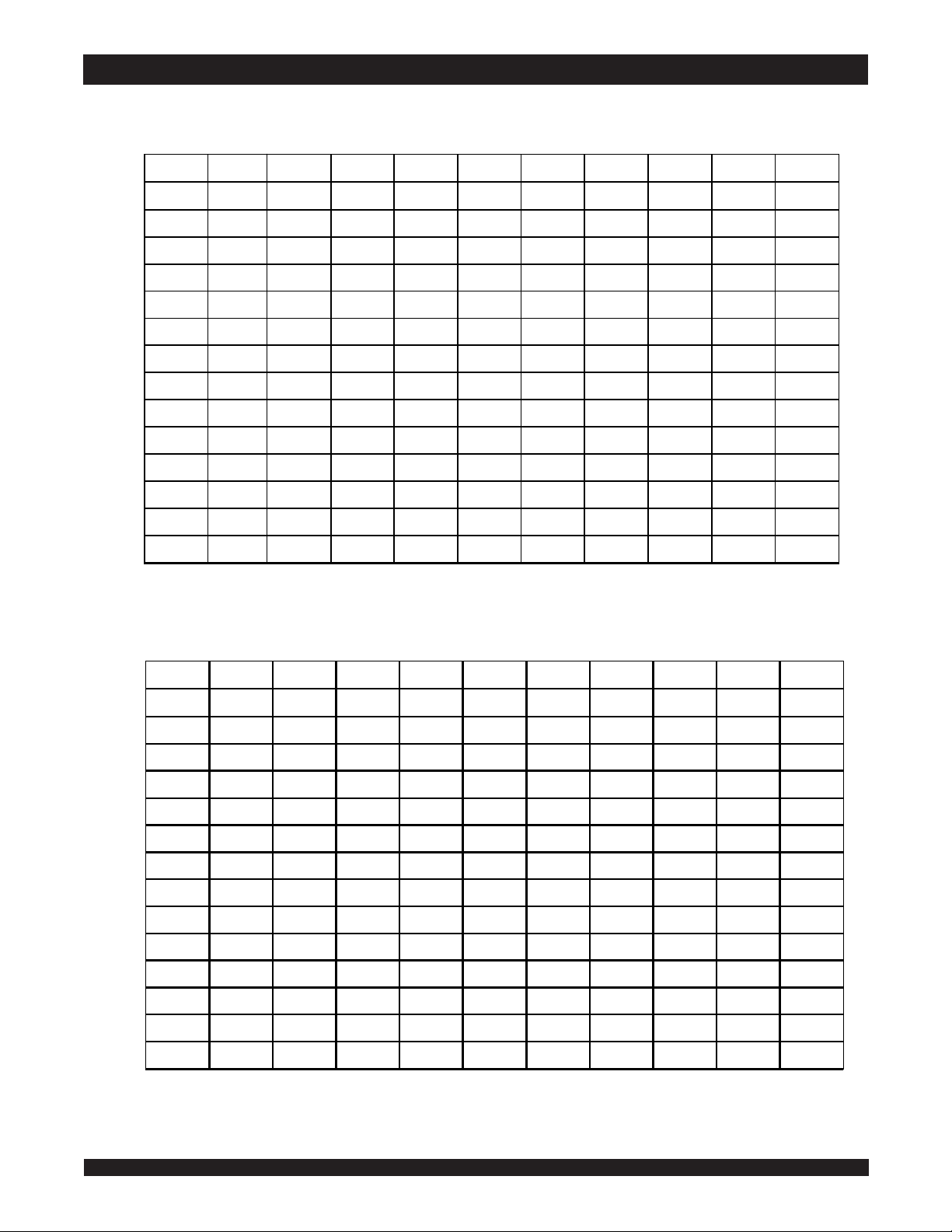
IDT71V65602, IDT71V65802, 256K x 36, 512K x 18, 3.3V Synchronous SRAMs with
R/WChip
(5)
Enable
ADV/
x
ADDRESS
USED
PREVIOUS CYCLE
CURRENT CYCLE
I/O
(2 cycles l ater)
OP ERATION
R/
1BW2BW3
(3)
4
(3)
READHXXXXWRITE ALL BYTES
LLLLL
WRITE BYTE 1 (I/O[0:7], I/O
P1
)
(2)
LLHHH
WRITE BYTE 2 (I/O[8:15], I/O
P2
)
(2)
LHLHH
WRITE BYTE 3 (I/O[16:23] , I/O
P3
)
(2,3)
LHHLH
WRITE BYTE 4 (I/O[24:31] , I/O
P4
)
(2,3)
LHHHL
NO WRITE
LHHHH
5303 tbl 09
ZBT
Feature, 2.5V I/O, Burst Counter, and Pipelined Outputs Commercial and Industrial Temperature Ranges
Synchronous Truth Table
CEN
LD
(1)
BW
D
Q
HiZ
(7)
(7)
(7)
(7)
L L Se le ct L Valid Ex ternal X LOAD WRITE D
L H Sele ct L X Ex ternal X LOAD READ Q
L X X H Valid Inte r nal LOA D WRITE /
BURS T WRITE
L X X H X I nte rnal LOAD RE AD /
BURST READ
L X Deselect L X X X DESELECT or STOP
BURS T WRITE
(Advance burst counter)
BURST READ
(Advance burst counter)
(2)
(2)
(3)
L X X H X X DESELECT / NOOP NOOP HiZ
H X X X X X X SUS PE ND
NOTES:
1. L = VIL, H = VIH, X = Don’t Care.
2. When ADV/LD signal is sampled high, the internal burst counter is incremented. The R/ W signal is ignored when the counter is advanced. Therefore the nature of
the burst cycle (Read or Write) is determined by the status of the R/W signal when the first address is loaded at the beginning of the burst cycle.
3. Deselect cycle is initiated when either (CE1, or CE2 is sampled high or CE2 is sampled low) and ADV/LD is sampled low at rising edge of clock. The data bus will
tri-state two cycles after deselect is initiated.
4. When CEN is sampled high at the rising edge of clock, that clock edge is blocked from propogating through the part. The state of all the internal registers and the I/
Os remains unchanged.
5. To select the chip requires CE1 = L, CE2 = L, CE2 = H on these chip enables. Chip is deselected if any one of the chip enables is false.
6. Device Outputs are ensured to be in High-Z after the first rising edge of clock upon power-up.
7. Q - Data read from the device, D - data written to the device.
(4)
Previous Value
5303 tbl 08
Partial Truth Table for Writes
NOTES:
1. L = VIL, H = VIH, X = Don’t Care.
2. Multiple bytes may be selected during the same cycle.
3. N/A for X18 configuration.
(1)
W
BW
BW
6.42
9
 Loading...