

IDT IDT71V3576S User Manual
查询IDT71V3576S133BG供应商
128K x 36, 256K x 18
3.3V Synchronous SRAMs
3.3V I/O, Pipelined Outputs
Burst Counter, Single Cycle Deselect
Features
◆◆
◆
◆◆
128K x 36, 256K x 18 memory configurations
◆◆
◆
◆◆
Supports high system speed:
Commercial and Industrial:
– 150MHz 3.8ns clock access time
– 133MHz 4.2ns clock access time
◆◆
◆
◆◆
LBO input selects interleaved or linear burst mode
◆◆
◆
◆◆
Self-timed write cycle with global write control (GW), byte write
enable (BWE), and byte writes (BWx)
◆◆
◆
◆◆
3.3V core power supply
◆◆
◆
◆◆
Power down controlled by ZZ input
◆◆
◆
◆◆
3.3V I/O
◆◆
◆
◆◆
Optional - Boundary Scan JTAG Interface (IEEE 1149.1
compliant)
◆◆
◆
◆◆
Packaged in a JEDEC Standard 100-pin plastic thin quad
flatpack (TQFP), 119 ball grid array (BGA) and 165 fine pitch ball
grid array (fBGA)
IDT71V3576S
IDT71V3578S
IDT71V3576SA
IDT71V3578SA
Description
The IDT71V3576/78 are high-speed SRAMs organized as
128K x 36/256K x 18. The IDT71V3576/78 SRAMs contain write, data,
address and control registers. Internal logic allows the SRAM to generate
a self-timed write based upon a decision which can be left until the end of
the write cycle.
The burst mode feature offers the highest level of performance to the
system designer, as the IDT71V3576/78 can provide four cycles of data
for a single address presented to the SRAM. An internal burst address
counter accepts the first cycle address from the processor, initiating the
access sequence. The first cycle of output data will be pipelined for one
cycle before it is available on the next rising clock edge. If burst mode
operation is selected (ADV=LOW), the subsequent three cycles of output
data will be available to the user on the next three rising clock edges. The
order of these three addresses are defined by the internal burst counter
and the LBO input pin.
The IDT71V3576/78 SRAMs utilize IDT’s latest high-performance
CMOS process and are packaged in a JEDEC standard 14mm x 20mm
100-pin thin plastic quad flatpack (TQFP) as well as a 119 ball grid array
(BGA) and a 165 fine pitch ball grid array (fBGA).
Pin Description Summary
17
A0-A
CE
0
1
CS
, CS
OE
GW
BWE
BW
(1)
3
4
,
BW
P4
1
2
,
,
BW
BW
CLK Clo c k Inp ut N/A
ADV
ADSC
ADSP
LBO
TMS Test Mode Select Input Synchronous
TDI Tes t Data Inp ut Inp ut Sy nc hro no us
TCK Test Clock Input N/A
TDO Test Da ta Outp u t Outp ut Sy nc hro n o us
TRST
ZZ Sleep Mode Input Asynchronous
0
I/O
-I/O31, I/OP1-I/O
DDQ
VDD, V
SS
V
NOTE:
1. BW3 and BW4 are not applicable for the IDT71V3578.
©2003 Integrated Device Technology, Inc.
Ad d re s s Inputs Inp ut Sy nc hro no us
Chip Enable Input Synchronous
Chip Se le c ts Input Sy nc hron ou s
Output Enable Input Asynchronous
Global Write Enable Input Synchronous
Byte Write E nable Input Synchrono us
Indi vi d ual B y te Write S el e c ts Input Sy nc hro no us
Burs t Ad d re s s Ad v anc e Input Sy nc hro no us
Ad d res s Status (Cac he Co ntrol le r) Input Sy nc hron ou s
Address Status (Processor) Input Synchronous
Linear / Interle aved Burst Orde r Input DC
JTAG Res e t (Op tio na l) Input A sy nc hro no us
Data Inp ut / Outp ut I/O Sy nc hro no us
Co re P o we r, I/ O P o we r Sup p l y N/A
Ground Supply N/A
JUNE 2003
1
52 79 tb l 01
DSC-5279/03
IDT71V3576, IDT71V3578, 128K x 36, 256K x 18, 3.3V Synchronous SRAMs with
Symbol
Pin Function
I/O
Active
Description
3.3V I/O, Pipelined Outputs, Burst Counter, Single Cycle Deselect Commercial and Industrial Temperature Ranges
Pin Definitions
(1)
A0-A
ADSC
ADSP
ADV
BWE
17
Address Inputs I N/A
Address Status
(Cach e Co ntro ll e r)
Address Status
(Processor)
Burst Address
Advance
I LOW
I LOW
I LOW
Byte Write E nable I LOW
Synchronous Address inputs. The address register is triggered by a combination of the rising edge
of CLK and ADSC Low o r ADSP Low and CE Low.
Synchronous Address Status from Cache Controller. AD SC is an activ e LOW inp ut that is use d to lo ad
the address registers with new addresses.
Synchronous Address Status from Processor. ADSP is an activ e LOW inp ut that is used to lo ad the
address registers with new addresses. ADSP is gated by CE.
Synchronous Address Advance. ADV is an ac tive LOW input that is use d to ad vanc e the internal b urst
counter, controlling burst access after the initial address is loaded. When the input is HIGH the burst
counter is not incremented; that is, there is no address advance.
Synchronous byte write enable gates the byte write inputs BW
1
-BW4. If BWE is LOW at the rising
edge of CLK then BWx inputs are passed to the next stage in the circuit. If BW E is HIG H the n the
byte write inputs are blocked and only GW can initiate a write cycle.
BW
1
CE
-BW
4
Individual Byte
Write Enable s
I LOW
Chip E nable I LOW
Synchronous byte write enables. BW1 controls I/O
byte write causes all outputs to be disabled.
0
Synchronous chip enable. CE is use d wi th CS
and CS1 to enab le the IDT71V3576/78. CE also g ate s
ADSP.
0-7
, I/OP1, BW2 controls I/O
8-15
, I/OP2, etc. Any active
CLK Clock I N/A This is the clock input. All timing references for the device are made with respect to this input.
CS
CS
GW
0
-I/O
I/O
I/OP1-I/O
0
1
31
P4
Chip Select 0 I HIGH Synchronous active HIGH chip select. CS0 is used with CE and CS1 to enable the chip .
Chip S e le ct 1 I LOW Sync hro no us active LOW c hip se le c t. CS1 is used with CE and CS0 to enable the chip .
Global Write
Enabl e
I LOW
Data Inp ut/Outp ut I/O N/A
Synchronous global write enable. This input will write all four 9-bit data bytes when LOW on the rising
edge of CLK. GW supersedes individual byte write enables.
Synchronous data input/output (I/O) pins. Both the data input path and data output path are registered
and triggered by the rising edge of CLK.
Asynchronous burst order selection input. When LBO is HIGH, the interleaved burst sequence is
LBO
Linear B urst Orde r I LOW
selected. When LBO is LOW the Linear burst sequence is selected. LBO is a static input and must
not change state while the device is operating.
OE
Output Enabl e I LOW
TMS Test ModeSelect I N/A
TDI Test Data Inp ut I N/A
TCK Te s t Cl o ck I N/ A
TDO Test DataOutput O N/A
TRST
JTAG Re set
(Optio nal )
I LOW
Asy nchro nous outp ut enab le . When OE is LOW the data output drivers are enabled on the I/O pins if
the chip is also selected. When OE is HIGH the I/O pins are in a high-impedance state.
Gives input command for TAP controller. Sampled on rising edge of TDK. This pin has an internal
pullup.
Serial input of registers placed between TDI and TDO. Sampled on rising edge of TCK. This pin has
an internal p ullup .
Clock input of TAP controller. Each TAP event is clocked. Test inputs are captured on rising edge of
TCK, while test outputs are driven from the falling edge of TCK. This pin has an internal pullup.
Serial o utput of registers placed between TDI and TDO. This output is active depending on the state
of the TAP controller.
Optional Asynchronous JTAG reset. Can be used to reset the TAP controller, but not required. JTAG
reset occurs automatically at p o wer up and also resets using TMS and TCK per IEEE 1149.1. If not
use d TRST can be left floating . This p in has an i nternal pullup. Only available in BGA package .
Asynchronous sleep mode input. ZZ HIGH will gate the CLK internally and power down the
ZZ Sleep Mode I HIGH
IDT71V 3576/78 to i ts lo west p o wer co nsum ptio n le ve l. Data re tentio n is g uarantee d i n Sle ep
Mode.This pin has an internal pull down.
V
DD
DDQ
V
SS
V
Power Supply N/A N/A 3.3V core power supply.
Power Supply N/A N/A 3.3V I/O Supply.
Ground N/A N/A Ground.
NC No Co nne c t N/ A N/A NC pi ns are no t e le c tric al ly c o nne c te d to the d e v ic e .
NOTE:
1. All synchronous inputs must meet specified setup and hold times with respect to CLK.
5279 tbl 02
6.42
2
IDT71V3576, IDT71V3578, 128K x 36, 256K x 18, 3.3V Synchronous SRAMs with
3.3V I/O, Pipelined Outputs, Burst Counter, Single Cycle Deselect Commercial and Industrial Temperature Ranges
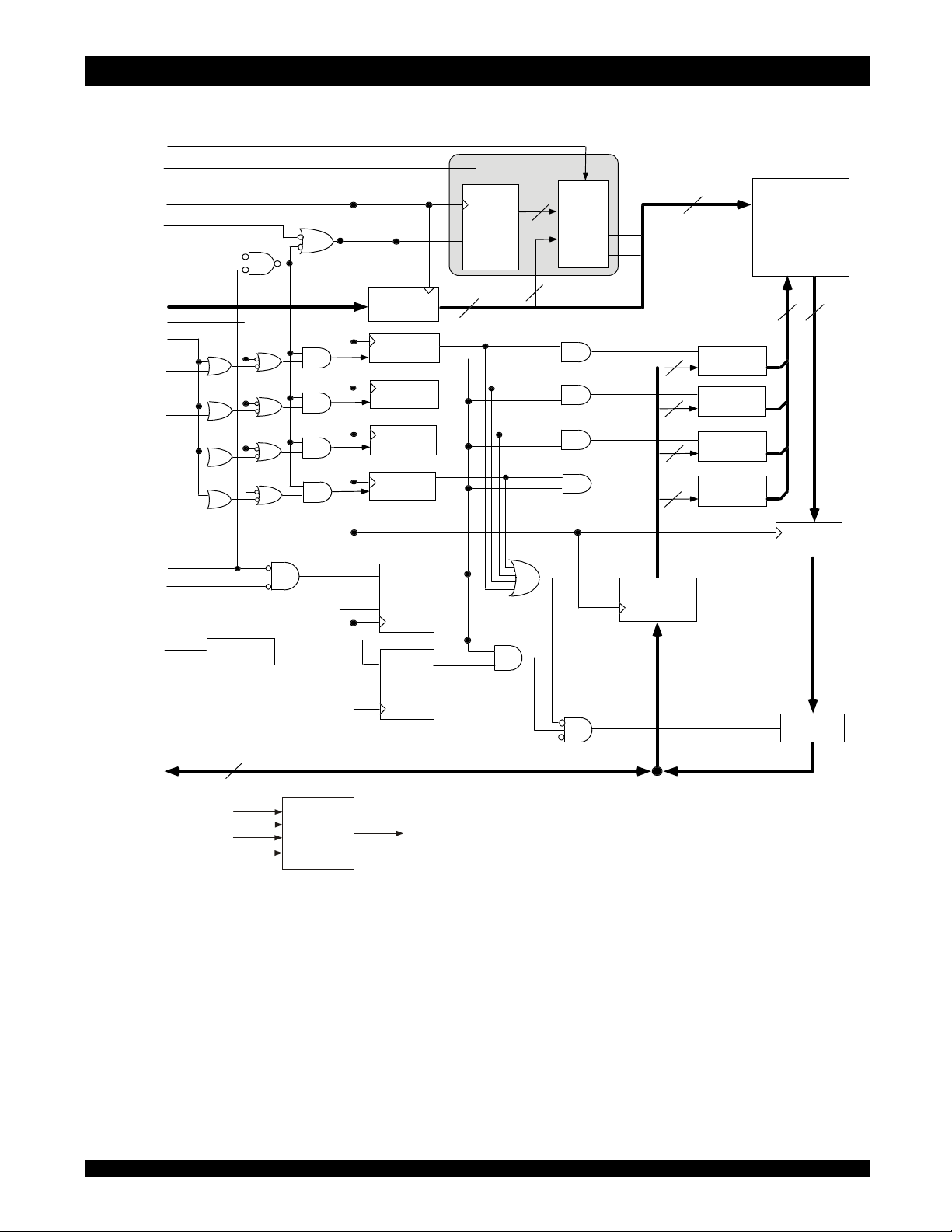
Functional Block Diagram
LBO
ADV
CLK
ADSC
ADSP
CEN
CLR
Binary
Counter
Burst
Sequence
2
Burst
Logic
Q0
Q1
A0*
A1*
INTERNAL
ADDRESS
17/18
128K x 36/
256K x 18-
BIT
MEMORY
ARRAY
A0-A
BWE
BW
BW
BW
BW
I/O0—I/O
I/OP1— I/O
16/17
GW
CE
CS
CS
ZZ
OE
1
2
3
4
0
1
31
P4
Powerdown
36/18
TMS
TDI
TCK
TRST
(Optional)
JTAG
(SA Version)
CLK EN
ADDRESS
REGISTER
Byte 1
Write Register
Byte 2
Write Register
Byte 3
Write Register
Byte 4
Write Register
Q
D
Enable
Register
CLK EN
DQ
Enable
Delay
Register
TDO
17/18
2
1
A0,A
2–A17
A
9
9
9
9
DATA INPUT
REGISTER
Byte 1
Write Driver
Byte 2
Write Driver
Byte 3
Write Driver
Byte 4
Write Driver
36/18
OE
OUTPUT
REGISTER
OUTPUT
BUFFER
36/18
,
5279 drw 01
6.42
3
IDT71V3576, IDT71V3578, 128K x 36, 256K x 18, 3.3V Synchronous SRAMs with
Symbol
Rating
Commercial &
Ind ustrial
Unit
V
(2 )
Te rminal Voltag e with
Re s p e c t to G ND
-0.5 to +4.6
V
V
(3,6)
Te rminal Voltag e with
Re s p e c t to G ND
-0.5 to V
V
V
(4,6)
Te rminal Voltag e with
Re s p e c t to G ND
-0.5 to V
+0.5
V
V
(5,6)
Te rminal Voltag e with
Re s p e c t to G ND
-0.5 to V
+0.5
V
T
Commercial
Operating Temperature
-0 to + 70
C
Industrial
Operating Temperature
-40 to + 85
C
T
Temperature
Unde r Bi as
-55 to + 125
C
T
Storage
Temperature
-55 to + 125
C
PTPo wer Di ss ip atio n
2.0WI
DC Output Current
50
mA
5279 t bl 03
Grade
Temperature
(1)
VSSVDDV
DDQ
Symbol
Par ameter
Min.
Typ.
Max.
Unit
(1)
(1)
5279 tbl 07a
(1)
3.3V I/O, Pipelined Outputs, Burst Counter, Single Cycle Deselect Commercial and Industrial Temperature Ranges
Absolute Maximum Ratings
(1)
Recommended Operating
Temperature and Supply Voltage
TE RM
TE RM
TE RM
TE RM
(7)
A
BIAS
STG
OUT
NOTES:
1. Stresses greater than those listed under ABSOLUTE MAXIMUM RATINGS may
cause permanent damage to the device. This is a stress rating only and functional
operation of the device at these or any other conditions above those indicated
in the operational sections of this specification is not implied. Exposure to absolute
maximum rating conditions for extended periods may affect reliability.
2. VDD terminals only.
3. VDDQ terminals only.
4. Input terminals only.
5. I/O terminals only.
6. This is a steady-state DC parameter that applies after the power supplies have
ramped up. Power supply sequencing is not necessary; however, the voltage
on any input or I/O pin cannot exceed VDDQ during power supply ramp up.
7. TA is the "instant on" case temperature.
DD
DD
DDQ
o
o
o
o
Com me rc ial 0°C to + 70° C 0V 3. 3V ± 5% 3. 3V ± 5%
Industrial -40°C to +85° C 0V 3.3V ± 5% 3.3V±5%
NOTES:
1. TA is the "instant on" case temperature.
5279 tbl 04
Recommended DC Operating
Conditions
VDDCore Supply Voltage 3.135 3.3 3.465 V
DDQ
I/O Supply Voltage 3.135 3.3 3.465 V
V
SS
Sup ply Volt ag e 0 0 0 V
V
IH
Input High Voltage - In puts 2. 0
V
Input High Voltage - I/ O 2. 0
V
IH
IL
Input Low Voltage -0.3
V
NOTES:
1. VIH (max) = VDDQ + 1.0V for pulse width less than tCYC/2, once per cycle.
2. VIL (min) = -1.0V for pulse width less than tCYC/2, once per cycle.
____
DD
V
+0.3 V
____
V
(2 )
____
+0.3
DDQ
0.8 V
(1)
5279 tbl 06
V
100 Pin TQFP Capacitance
(TA = +25°C, f = 1.0MHz)
Symbol Parameter
165 fBGA Capacitance
(TA = +25°C, f = 1.0MHz)
Symbol Para met er
NOTE:
1. This parameter is guaranteed by device characterization, but not production tested.
Conditions Max. Unit
Inp ut Cap a ci tanc e VIN = 3dV 5 pF
C
IN
C
I/O Cap ac ita nce V
I/O
= 3dV 7 pF
OUT
Conditions Max. Unit
C
Inp ut Ca p ac ita nc e VIN = 3dV 7 p F
IN
I/O Cap ac itan ce V
C
I/O
= 3dV 7 pF
OUT
5279 tbl 07
5279 tb l 07b
6.42
4
119 BGA Capacitance
(TA = +25°C, f = 1.0MHz)
Symbol Pa ra met er
C
Inp ut Cap ac ita nce VIN = 3dV 7 pF
IN
C
I/O Cap ac i tanc e V
I/O
Conditions Max. Unit
= 3dV 7 p F
OUT
IDT71V3576, IDT71V3578, 128K x 36, 256K x 18, 3.3V Synchronous SRAMs with
3.3V I/O, Pipelined Outputs, Burst Counter, Single Cycle Deselect Commercial and Industrial Temperature Ranges
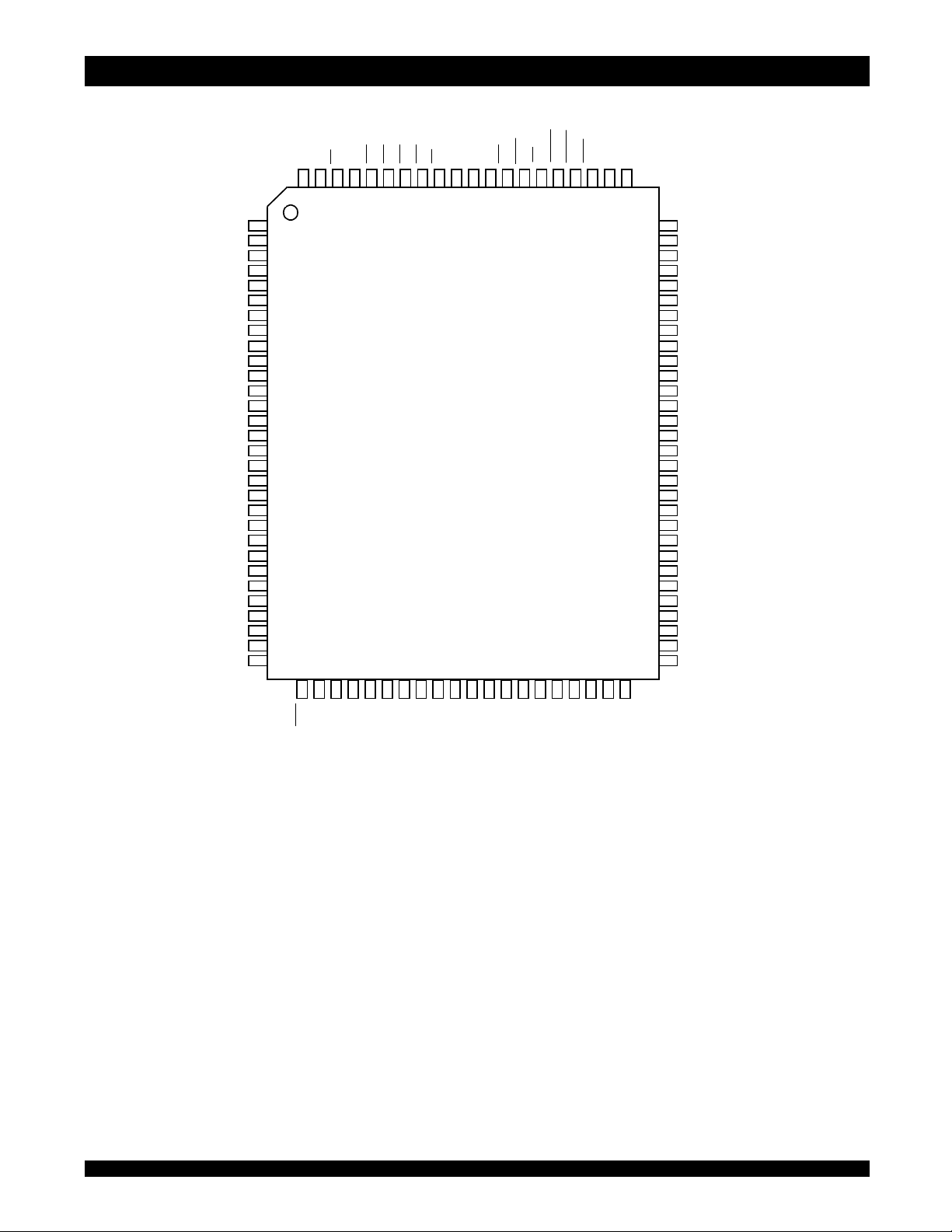
Pin Configuration 128K x 36
C
4
3
2
0
7
A6A
10099989796959493929190 8786858483828189 88
W
E
S
B
C
C
1
1
D
S
LK
D
W
W
W
B
B
B
S
S
C
C
V
V
E
W
W
B
G
P
S
V
S
E
D
A
O
8A9
D
D
A
A
A
I/O
I/O
I/O
V
DDQ
V
I/O
I/O
I/O
I/O
V
V
DDQ
I/O
I/O
VDD/NC
V
V
I/O
I/O
V
DDQ
V
I/O
I/O
I/O
I/O
V
V
DDQ
I/O
I/O
I/O
NC
P3
SS
SS
DD
SS
SS
SS
P4
1
2
16
3
17
4
5
6
18
7
19
8
20
9
21
10
11
12
22
13
23
(1)
14
15
16
17
18
24
19
25
20
21
22
26
23
27
24
28
25
29
26
27
28
30
29
31
30
31 32 33 34 35 36 37 38 39 40 41 42 43 44 45 46 47 48 49 50
O
LB
5
A0A1A2A3A4A
S
D
C
C
C
S
N
N
V
C
D
N
N
V
80
I/O
I/O
I/O
V
V
SS
I/O
I/O
I/O
I/O
V
V
I/O
I/O
V
NC
V
DD
ZZ
I/O
I/O
V
DDQ
V
SS
I/O
I/O
I/O
I/O
V
V
I/O
I/O
I/O
5279 drw 02
15
14
DDQ
13
12
11
10
SS
DDQ
9
8
SS
(2)
7
6
5
4
3
2
SS
DDQ
1
0
P2
,
P1
79
78
77
76
75
74
73
72
71
70
69
68
67
66
65
64
63
62
61
60
59
58
57
56
55
54
53
52
51
14A13A12A11A10
16
A15A
A
TQFP
Top View
NOTES:
1. Pin 14 can either be directly connected to VDD, or connected to an input voltage ≥ VIH, or left unconnected.
2. Pin 64 can be left unconnected and the device will always remain in active mode.
6.42
5
IDT71V3576, IDT71V3578, 128K x 36, 256K x 18, 3.3V Synchronous SRAMs with
3.3V I/O, Pipelined Outputs, Burst Counter, Single Cycle Deselect Commercial and Industrial Temperature Ranges
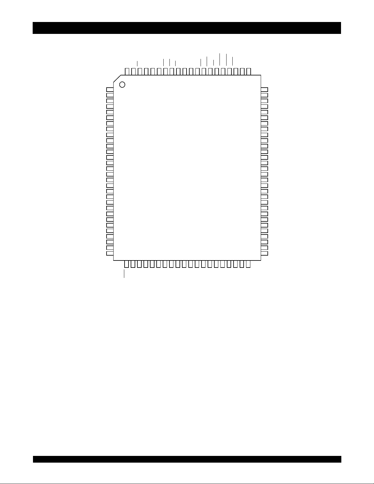
Pin Configuration 256K x 18
C
2
0
7
A6A
10099989796959493929190 8786858483828189 88
C
S
E
N
C
C
1
1
D
S
C
W
W
S
B
N
B
C
LK
D
S
C
V
V
E
W
W
B
G
P
S
V
S
E
D
A
O
8A9
D
D
A
A
A
DDQ
V
V
I/O
I/O
V
DDQ
V
I/O
I/O
VDD/NC
V
V
I/O
I/O
DDQ
V
V
I/O
I/O
I/O
V
DDQ
V
NC
NC
NC
NC
NC
NC
NC
NC
NC
NC
SS
SS
DD
SS
SS
P2
SS
1
2
3
4
5
6
7
8
8
9
9
10
11
12
10
13
11
(1)
14
15
16
17
18
12
19
13
20
21
22
14
23
15
24
25
26
27
28
29
30
31 32 33 34 35 36 37 38 39 40 41 42 43 44 45 46 47 48 49 50
O
LB
5
A0A1A2A3A4A
S
D
C
C
C
C
S
D
N
N
N
N
V
V
80
79
78
77
76
75
74
73
71
69
67
66
65
64
62
61
60
59
58
57
56
54
53
52
15A14A13A12A11
17
A
A16A
72
70
68
63
55
51
5279 drw 03
A
NC
NC
V
V
NC
I/O
I/O
I/O
V
V
I/O
I/O
V
NC
V
ZZ
I/O
I/O
V
V
I/O
I/O
NC
NC
V
V
NC
NC
NC
10
DDQ
SS
P1
7
6
SS
DDQ
5
4
SS
DD
(2)
DDQ
SS
1
0
SS
DDQ
3
2
,
TQFP
Top View
NOTES:
1. Pin 14 can either be directly connected to VDD, or connected to an input voltage ≥ VIH, or left unconnected.
2. Pin 64 can be left unconnected and the device will always remain in active mode.
6.42
6
IDT71V3576, IDT71V3578, 128K x 36, 256K x 18, 3.3V Synchronous SRAMs with
3.3V I/O, Pipelined Outputs, Burst Counter, Single Cycle Deselect Commercial and Industrial Temperature Ranges
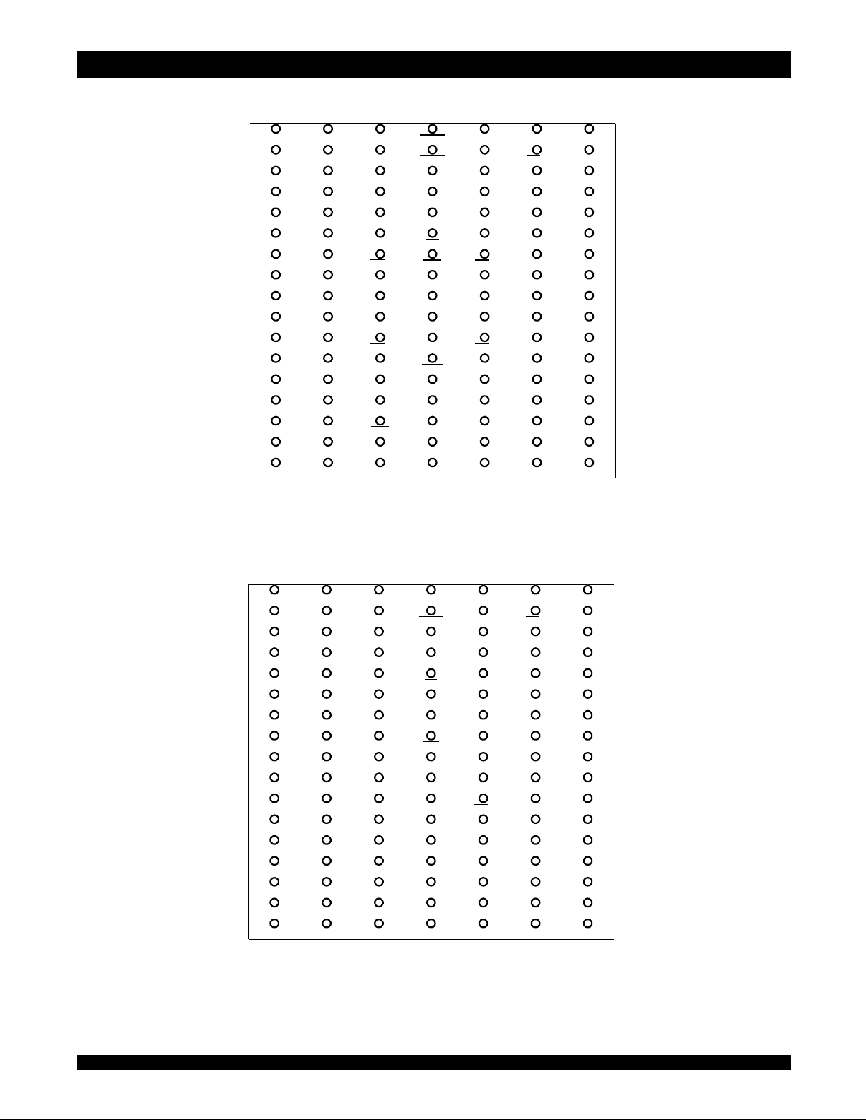
Pin Configuration 128K x 36, 119 BGA
1234567
DDQ
V
A
NC
B
NC
C
16
I/O
D
17
I/O
E
DDQ
V
F
20
I/O
G
22
I/O
H
DDQ
V
J
24
I/O
K
25
I/O
L
DDQ
V
M
29
I/O
N
31
I/O
P
NC A
R
NC NC A
T
DDQ
V
U
6
A
CS
7
A
P3
I/O
18
I/O
19
I/O
21
I/O
23
I/O
DD
V
26
I/O
27
I/O
28
I/O
30
I/O
P4
I/O
5
NC/TMS
0
(2)
4
A
3
A
2
A
SS
V
SS
V
SS
V
3
BW
SS
V
NC V
SS
V
4
BW
SS
V
SS
V
SS
V
LBO
10
(2)
NC/TDI
ADSP
ADSC
DD
V
NC V
CE
OE
ADV BW
GW
DD
CLK V
NC
BWE
1
A
0
A
DD
V
11
A
(2)
NC/TCK
8
A
9
A
12
A
SS
SS
V
SS
V
2
SS
V
NC V
SS
1
BW
SS
V
SS
V
SS
V
DD
/NC
V
14
A
NC/TDO
(1)
(2)
16
A
1
CS
15
A
P2
I/O
13
I/O
12
I/O
11
I/O
9
I/O
DD
6
I/O
4
I/O
3
I/O
2
I/O
0
I/O
13
A
NC
NC/TRST
(2,3)
DDQ
V
NC
NC
15
I/O
14
I/O
DDQ
V
10
I/O
8
I/O
DDQ
V
7
I/O
5
I/O
DDQ
V
1
I/O
P1
I/O
NC
(4)
ZZ
DDQ
V
5279 drw 04
,
Top View
Pin Configuration 256K x 18, 119 BGA
1234567
DDQ
V
A
NC CS
B
NC
C
8
I/O
D
NC I/O
E
DDQ
V
F
NC I/O
G
11
I/O
H
DDQ
V
J
NC I/O
K
13
I/O
L
DDQ
V
M
15
I/O
N
NC I/O
P
NC A
R
NC A
T
DDQ
V
U
NOTES:
1. R5 can either be directly connected to VDD, or connected to an input voltage ≥ VIH, or left unconnected.
2. These pins are NC for the "S" version or the JTAG signal listed for the "SA" version. Note: If NC, these pins can either be tied to VSS, VDD or left floating.
3. TRST is offered as an optional JTAG Reset if required in the application. If not needed, can be left floating and will internally be pulled to VDD.
4. T7 can be left unconnected and the device will always remain in active mode.
6
A
0
7
A
NC V
9
NC V
10
NC V
DD
V
12
NC NC
14
I/O
NC V
P2
5
10
NC/TMS
(2)
4
A
3
A
2
A
SS
SS
V
SS
BW
SS
NC V
SS
V
SS
V
SS
V
SS
SS
V
LBO
15
A
NC/TDI
2
(2)
Top View
ADSP
ADSC
DD
V
NC V
CE
OE
ADV
GW
DD
CLK V
BWE
1
A
0
A
DD
V
NC A
NC/TCK
(2)
8
A
9
A
13
A
SS
SS
V
SS
V
SS
V
SS
V
NC V
SS
1
BW
SS
V
SS
V
SS
V
DD
V
/NC
14
NC/TDO
(1)
(2)
NC/TRST
16
A
CS
A
I/O
V
1
17
7
NC I/O
5
I/O
V
NC I/O
3
I/O
DD
V
NC I/O
1
I/O
NC V
0
I/O
NC I/O
12
A
11
A
(2,3)
V
DDQ
NC
NC
NC
6
DDQ
4
NC
DDQ
2
NC
DDQ
NC
P1
NC
(4)
ZZ
DDQ
5279 drw 05
,
6.42
7
 Loading...