

IDT IDT71V2576, IDT71V2578 User Manual
查询IDT71V2576供应商
128K X 36, 256K X 18
3.3V Synchronous SRAMs
2.5V I/O, Pipelined Outputs,
Burst Counter , Single Cycle Deselect
Features
◆◆
◆
◆◆
128K x 36, 256K x 18 memory configurations
◆◆
◆
◆◆
Supports high system speed:
Commercial and Industrial:
– 150MHz 3.8ns clock access time
– 133MHz 4.2ns clock access time
◆◆
◆
◆◆
LBO input selects interleaved or linear burst mode
◆◆
◆
◆◆
Self-timed write cycle with global write control (GW), byte write
enable (BWE), and byte writes (BWx)
◆◆
◆
◆◆
3.3V core power supply
◆◆
◆
◆◆
Power down controlled by ZZ input
◆◆
◆
◆◆
2.5V I/O
◆◆
◆
◆◆
Packaged in a JEDEC Standard 100-pin plastic thin quad
flatpack (TQFP), 119 ball grid array (BGA) and 165 fine pitch ball
grid array (fBGA)
IDT71V2576
IDT71V2578
Description
The IDT71V2576/78 are high-speed SRAMs organized as 128K x
36/256K x 18. The IDT71V2576/78 SRAMs contain write, data, address
and control registers. Internal logic allows the SRAM to generate a selftimed write based upon a decision which can be left until the end of the write
cycle.
The burst mode feature offers the highest level of performance to the
system designer, as the IDT71V2576/78 can provide four cycles of data
for a single address presented to the SRAM. An internal burst address
counter accepts the first cycle address from the processor, initiating the
access sequence. The first cycle of output data will be pipelined for one
cycle before it is available on the next rising clock edge. If burst mode
operation is selected (ADV=LOW), the subsequent three cycles of output
data will be available to the user on the next three rising clock edges. The
order of these three addresses are defined by the internal burst counter
and the LBO input pin.
The IDT71V2576/78 SRAMs utilize IDT’s latest high-performance
CMOS process and are packaged in a JEDEC standard 14mm x 20mm
100-pin thin plastic quad flatpack (TQFP) as well as a 119 ball grid array
(BGA) and 165 fine pitch ball grid array (fBGA).
Pin Description Summary
17
A0-A
CE
0
1
, CS
CS
OE
GW
BWE
BW
1
2
,
,
BW
BW
(1)
3
4
,
BW
CLK Clo c k Inp ut N/A
ADV
ADSC
ADSP
LBO
ZZ Sleep Mode Input Asynchronous
0
I/O
-I/O31, I/OP1-I/O
DDQ
VDD, V
SS
V
NOTE:
1. BW3 and BW4 are not applicable for the IDT71V2578.
©2003 Integrated Device Technology, Inc.
P4
Address Inputs Input Synchronous
Chip Enable Input Synchronous
Chip Se le cts Input S ync hrono us
Output Enable Input Asy nchrono us
Global Write Enable Input Synchronous
Byte Write Enable Input Synchronous
Indivi dual B yte Write Se le cts Input S ync hrono us
Burst Ad dre ss Ad vanc e Input S ync hrono us
Add re ss Status (Cache Co ntrolle r) Input S ync hrono us
Add re ss Status (Proc es so r) Input S ync hrono us
Li ne ar / Inte r le av e d B urs t Or d e r Inp ut DC
Data In p ut / Outp ut I/O Sy nc h ro no us
Co re Po we r, I/O P o we r Sup p l y N/A
Ground Supply N/A
APRIL 2003
1
DSC-4876/08
4876 t bl 01
IDT71V2576, IDT71V2578, 128K x 36, 256K x 18, 3.3V Synchronous SRAMs with
Symbol
Pin Function
I/O
Acti ve
Descri pti on
2.5V I/O, Pipelined Outputs, Burst Counter, Single Cycle Deselect Commercial and Industrial Temperature Ranges
Pin Definitions
17
A0-A
Address Inputs I N/A Synchronous Address inputs. The address register is triggered by a combination of the
(1)
rising edge of CLK and ADSC Low or ADSP Low and CE Low.
ADSC
ADSP
ADV
Address Status
(Cache Co ntrol le r)
Address Status
(Processor)
Burst Address
Advance
I LOW Synchronous Address Status from Cache Controller. ADS C is an active LOW input that is
used to load the address registers with new addresses.
I LOW Synchronous Address Status from Processor. ADSP is an ac tiv e LOW inp ut that is us e d to
load the address registers with new addresses. ADSP is gated by CE.
I LOW Synchronous Addres s Advance. AD V i s an ac tiv e LOW inp ut that is us e d to ad v anc e the
internal burst counter, co ntrolling burst access after the initial address is loade d. When the
input is HIGH the burst counter is not incremented; that is, there is no address advance.
1
4
BW
BW
BWE
Byte Write Enable I LOW Synchronous byte write enable gates the byte write inputs
BWE
-
. If
is LOW at the
rising edge of CLK then BWx inputs are passed to the next stage in the circuit. If BW E is
HIGH then the byte write inputs are blocked and only GW can initiate a write cycle.
BW
1
CE
-BW
4
Ind i v idua l B y te
Write Enable s
I LOW Synchronous byte write enables. BW1 controls I/O
Any active byte write causes all outputs to be disabled.
Chip Enab le I LO W Sync hro no us c hip enab l e. CE is us ed with CS
0-7
, I/OP1, BW2 controls I/O
0
and CS1 to e nab le the IDT71V2576/ 78. CE
8-15
, I/OP2, etc.
als o g ate s ADSP.
CLK Clock I N/A This is the clock input. All timing references for the device are made with respect to this
input.
CS
CS
GW
0
I/O
-I/O
I/OP1-I/O
LBO
0
1
31
P4
Chip Select 0 I HIGH Synchrono us active HIGH chip select. CS0 is us ed with CE and CS1 to enable the chip.
Chip Sele ct 1 I LOW Synchronous active LOW chip select. CS1 is us ed with CE and CS0 to enable the chip.
Glob al Write
Enable
I LOW Synchronous global write enable. This input will write all four 9-bit data bytes when LOW
on the rising edge of CLK. GW supersedes individual byte write enables.
Data Input/Output I/O N/A Synchronous data input/output (I/O) pins. Both the data input path and data output path are
registered and triggered by the rising edge of CLK.
Linear Burst Order I LOW Asynchronous burst order selection input. When LBO is HIGH, the interleaved burst
sequence is selected. When
LBO
is LOW the Linear burst sequence is selected.
LBO
static input and must not change state while the device is operating.
OE
Output Enable I LOW Asy nchrono us o utput enabl e. When OE is LOW the data output drivers are enabled on the
I/O pins if the chip is also selected. When OE is HIGH the I/O p ins are in a hi g himpedance state.
DD
V
DDQ
V
SS
V
Power Supply N/A N/A 3.3V core power supply.
Power Supply N/A N/A 2.5V I/O Supply.
Ground N/A N/A Ground.
NC No Connect N/A N/A NC pins are not electrically connected to the device.
ZZ Sleep Mode I HIGH Asynchronous sleep mode input. ZZ HIGH will gate the CLK internally and power down the
IDT71V2576/78 to its lowes t power co nsum ption le vel. Data retention is guarante ed in
Sleep Mode.
NOTE:
1. All synchronous inputs must meet specified setup and hold times with respect to CLK.
4876 t bl 02
is a
6.42
2
IDT71V2576, IDT71V2578, 128K x 36, 256K x 18, 3.3V Synchronous SRAMs with
2.5V I/O, Pipelined Outputs, Burst Counter, Single Cycle Deselect Commercial and Industrial Temperature Ranges
Functional Block Diagram
LBO
ADV
CLK
ADSC
ADSP
CEN
CLR
Binary
Counter
Burst
Sequence
2
Burst
Logic
Q0
Q1
A0*
A1*
INTERNAL
ADDRESS
17/18
128K x 36/
256K x 18-
BIT
MEMORY
ARRAY
A0-A
BWE
BW
BW
BW
BW
I/O0—I/O
I/OP1— I/O
16/17
GW
CE
CS
CS
ZZ
OE
CLK EN
ADDRESS
REGISTER
Byte 1
Write Register
1
Byte 2
Write Register
2
3
4
0
1
Powerdown
31
P4
36/18
Byte 3
Write Register
Byte 4
Write Register
D
Enable
Register
CLK EN
DQ
Enable
Delay
Register
17/18
Q
2
1
A0,A
2-A17
A
9
9
9
9
DATA INPUT
REGISTER
Byte 1
Write Driver
Byte 2
Write Driver
Byte 3
Write Driver
Byte 4
Write Driver
36/18
OE
OUTPUT
REGISTER
OUTPUT
BUFFER
36/18
,
4876 drw 01
6.42
3
IDT71V2576, IDT71V2578, 128K x 36, 256K x 18, 3.3V Synchronous SRAMs with
Symbol
Rati ng
Commercial &
Industrial
Uni t
Commercial
Industrial
Grade
Temperature
(1)
VSSVDDV
DDQ
Symbol
Parameter
Min.
Typ.
Max.
Uni t
(1)
(1)
(1)
4876 tbl 07b
2.5V I/O, Pipelined Outputs, Burst Counter, Single Cycle Deselect Commercial and Industrial Temperature Ranges
Absolute Maximum Ratings
(1)
Recommended Operating
Temperature and Supply Voltage
(2)
TERM
V
TERM
V
TERM
V
TERM
V
(7)
A
T
BIAS
T
STG
T
T
P
OUT
I
NOTES:
1. Stresses greater than those listed under ABSOLUTE MAXIMUM RATINGS may
cause permanent damage to the device. This is a stress rating only and functional
operation of the device at these or any other conditions above those indicated
in the operational sections of this specification is not implied. Exposure to absolute
maximum rating conditions for extended periods may affect reliability.
2. VDD terminals only.
3. VDDQ terminals only.
4. Input terminals only.
5. I/O terminals only.
6. This is a steady-state DC parameter that applies after the power supplies have
ramped up. Power supply sequencing is not necessary; however, the voltage
on any input or I/O pin cannot exceed VDDQ during power supply ramp up.
7. TA is the "instant on" case temperature
Termi nal Vo ltag e with
-0.5 to +4.6 V
Re s p e c t to G ND
(3,6)
Termi nal Vo ltag e with
-0.5 to V
Re s p e c t to G ND
(4,6)
Termi nal Vo ltag e with
-0.5 to VDD +0.5 V
Re s p e c t to G ND
(5,6)
Termi nal Vo ltag e with
-0.5 to V
Re s p e c t to G ND
-0 to +7 0
Operating Temperature
-40 to + 85
Operating Temperature
T emperature
-55 to +125
Under Bias
Storage
-55 to +125
T emperature
Po we r Di ss ip ati o n 2.0 W
DC Output Curre nt 50 mA
DD
DDQ
+0.5 V
V
o
C
o
C
o
C
o
C
4876 t b l 03
Com me rc ial 0°C to + 70° C 0V 3.3V ± 5% 2.5V ± 5%
Industrial -40°C to +85° C 0V 3.3V± 5% 2.5V± 5%
NOTES:
1. TA is the "instant on" case temperature
4876 t b l 04
Recommended DC Operating
Conditions
DD
V
Core Sup p ly Vol tage 3. 135 3.3 3.465 V
DDQ
V
I/O Sup p ly Vol tage 2.375 2.5 2. 625 V
SS
V
Supply Voltage 0 0 0 V
Input High Voltage -
IH
V
1.7
____
Inputs
Inp ut Hi g h Vo l tag e - I/O
IH
V
IL
Inp ut L o w Vo lta g e -0.3
V
NOTES:
1. VIH (max) = VDDQ + 1.0V for pulse width less than tCYC/2, once per cycle.
2. VIL (min) = -1.0V for pulse width less than tCYC/2, once per cycle.
1.7
____
(2)
____
DD
V
+0.3
DDQ
V
(1)
+0.3
0.7 V
4876 t b l 05
V
V
100 TQFP Capacitance
(TA = +25°C, f = 1.0MHz)
Symbol Parameter
C
Inp ut Cap a ci tanc e VIN = 3dV 5 pF
IN
C
I/O Cap ac ita nce V
I/O
Conditions Max. Unit
= 3dV 7 pF
OUT
4876 tbl 07
119 BGA Capacitance
(TA = +25°C, f = 1.0MHz)
165 fBGA Capacitance
(TA = +25°C, f = 1.0MHz)
Symbol Para met e r
C
Inp ut Cap ac ita nce VIN = 3dV 7 pF
IN
C
I/O Cap ac i tanc e V
I/O
NOTE:
1. This parameter is guaranteed by device characterization, but not production tested.
Conditions Max. Unit
= 3dV 7 pF
OUT
6.42
4
Symbol Parameter
C
Inp ut Cap ac ita nc e VIN = 3dV 7 pF
IN
C
I/O Cap ac itanc e V
I/O
Conditions Max. Unit
= 3dV 7 pF
OUT
4876 tbl 07a
IDT71V2576, IDT71V2578, 128K x 36, 256K x 18, 3.3V Synchronous SRAMs with
2.5V I/O, Pipelined Outputs, Burst Counter, Single Cycle Deselect Commercial and Industrial Temperature Ranges
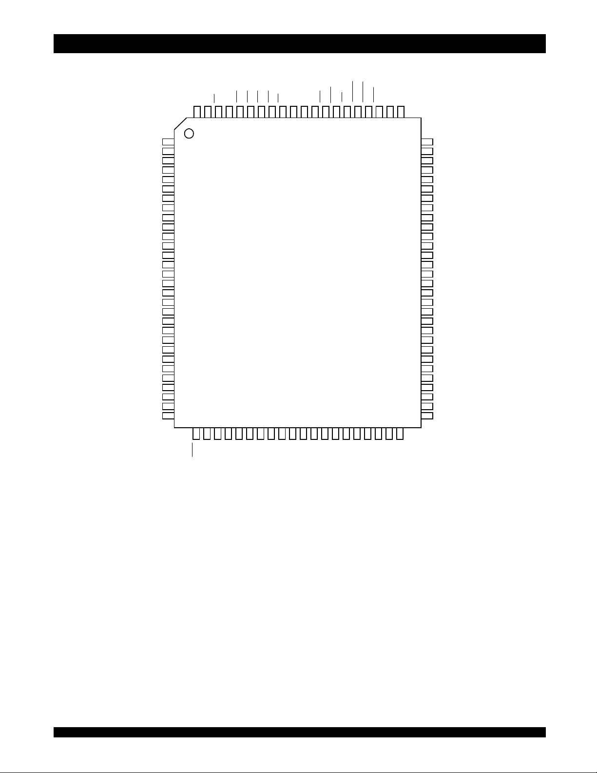
Pin Configuration 128K x 36
C
4
3
2
0
7
A6A
10099989796959493929190 8786858483828189 88
W
E
S
B
C
C
1
1
D
S
LK
D
W
W
W
B
B
B
S
S
C
C
V
V
E
W
W
B
G
P
S
V
S
E
D
A
O
8A9
D
D
A
A
A
I/O
I/O
I/O
V
I/O
I/O
I/O
I/O
V
I/O
I/O
VDD/NC
I/O
I/O
V
I/O
I/O
I/O
I/O
V
I/O
I/O
I/O
DDQ
V
SS
V
SS
DDQ
V
DD
NC
V
SS
DDQ
V
SS
V
SS
DDQ
1
P3
2
16
3
17
4
5
6
18
7
19
8
20
9
21
10
11
12
22
13
23
(1)
14
15
16
17
18
24
19
25
20
21
22
26
23
27
24
28
25
29
26
27
28
30
29
31
30
P4
31 32 33 34 35 36 37 38 39 40 41 42 43 44 45 46 47 48 49 50
O
LB
5
A0A1A2A3A4A
S
D
C
(2)
(2)
S
C
C
V
N
N
C
D
N
N
V
80
I/O
I/O
I/O
V
V
SS
I/O
I/O
I/O
I/O
V
SS
V
DDQ
I/O
I/O
V
SS
NC
V
DD
ZZ
I/O
I/O
V
DDQ
V
SS
I/O
I/O
I/O
I/O
V
SS
V
DDQ
I/O
I/O
I/O
4876 drw 02
15
14
DDQ
13
12
11
10
9
8
(3)
7
6
5
4
3
2
1
0
P2
P1
,
79
78
77
76
75
74
73
72
71
70
69
68
67
66
65
64
63
62
61
60
59
58
57
56
55
54
53
52
51
14A13A12A11A10
16
A15A
A
100 TQFP
Top View
NOTES:
1. Pin 14 can either be directly connected to VDD, or connected to an input voltage ≥ VIH, or left unconnected.
2. Pins 38 and 39 can be either NC or connected to VSS.
3. Pin 64 can be left unconnected and the device will always remain in active mode.
6.42
5
IDT71V2576, IDT71V2578, 128K x 36, 256K x 18, 3.3V Synchronous SRAMs with
2.5V I/O, Pipelined Outputs, Burst Counter, Single Cycle Deselect Commercial and Industrial Temperature Ranges
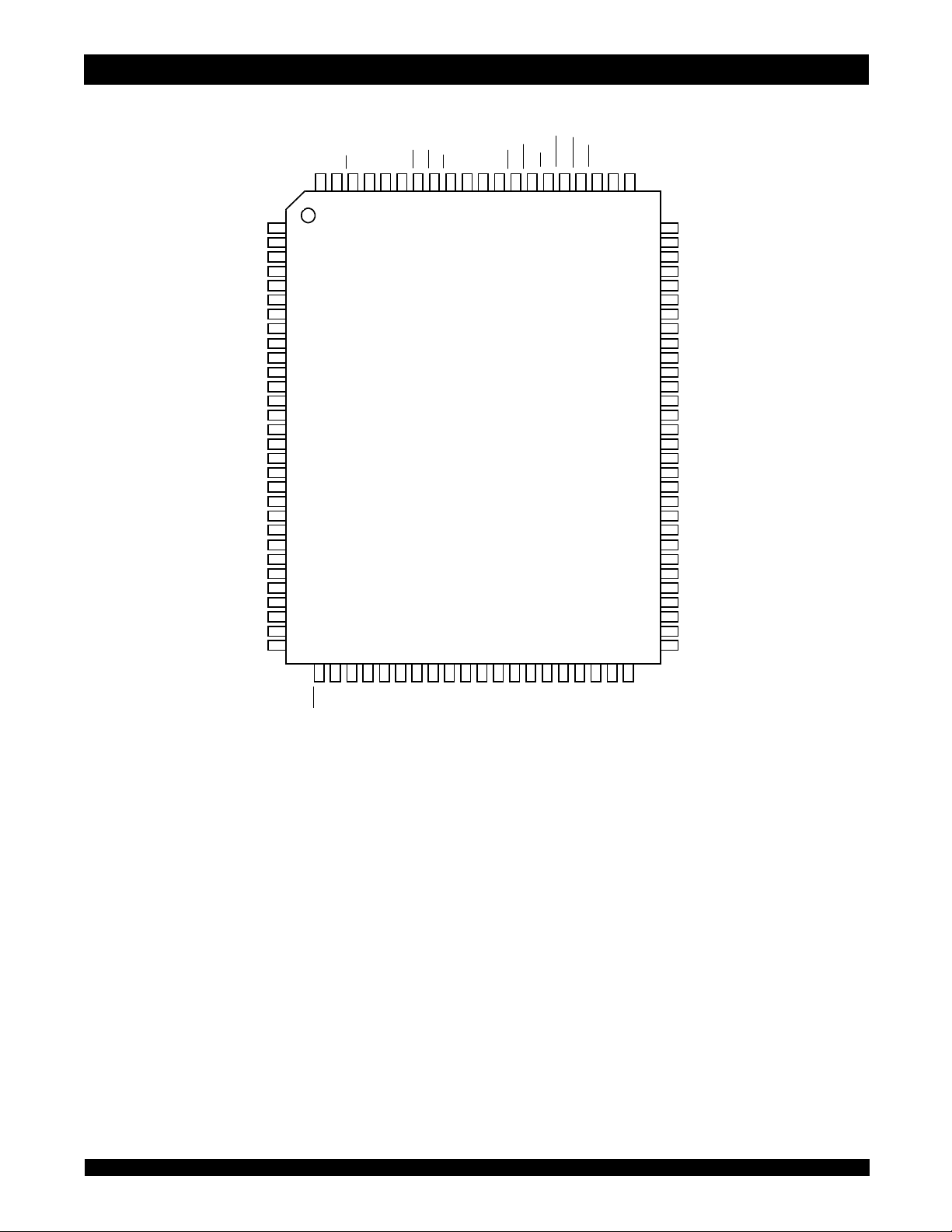
Pin Configuration 256K x 18
C
2
0
7
A6A
10099989796959493929190 8786858483828189 88
C
S
E
N
C
C
1
1
D
S
C
W
W
S
B
N
B
C
LK
D
S
C
V
V
E
W
W
B
G
P
S
V
S
E
D
A
O
8A9
D
D
A
A
A
V
V
I/O
I/O
VDD/NC
I/O
I/O
V
I/O
I/O
I/O
V
NC
NC
NC
DDQ
V
NC
NC
I/O
I/O
V
DDQ
V
NC
V
DDQ
V
NC
V
DDQ
NC
NC
NC
DD
1
2
3
4
5
SS
6
7
8
8
9
9
10
SS
11
12
10
13
11
(1)
14
15
16
17
SS
18
12
19
13
20
21
SS
22
14
23
15
24
P2
25
26
SS
27
28
29
30
31 32 33 34 35 36 37 38 39 40 41 42 43 44 45 46 47 48 49 50
O
LB
5
A0A1A2A3A4A
S
D
C
(2)
(2)
C
C
N
N
C
S
D
N
N
V
V
80
10
A
79
NC
78
NC
77
DDQ
V
76
SS
V
75
NC
74
73
72
71
70
69
68
67
66
65
64
63
62
61
60
59
58
57
56
55
54
53
52
51
15A14A13A12A11
17
A
A16A
I/O
I/O
I/O
V
V
I/O
I/O
V
NC
V
ZZ
I/O
I/O
V
V
I/O
I/O
NC
NC
V
V
NC
NC
NC
4876 drw 03
P1
7
6
SS
DDQ
5
4
SS
DD
(3)
3
2
DDQ
SS
1
0
SS
DDQ
,
100 TQFP
Top View
NOTES:
1. Pin 14 can either be directly connected to VDD, or connected to an input voltage ≥ VIH, or left unconnected.
2. Pins 38 and 39 can be either NC or connected to VSS.
3. Pin 64 can be left unconnected and the device will always remain in active mode.
6.42
6

IDT71V2576, IDT71V2578, 128K x 36, 256K x 18, 3.3V Synchronous SRAMs with
2.5V I/O, Pipelined Outputs, Burst Counter, Single Cycle Deselect Commercial and Industrial Temperature Ranges
Pin Configuration 128K x 36, 119 BGA
1234567
DDQ
V
A
NC CS
B
NC
C
16
I/O
D
17
I/O
E
DDQ
V
F
20
I/O
G
22
I/O
H
DDQ
V
J
24
I/O
K
25
I/O
L
DDQ
V
M
29
I/O
N
31
I/O
P
NC A
R
NC NC A
T
DDQ
V
U
A
A
I/O
I/O
I/O
I/O
I/O
V
I/O
I/O
I/O
I/O
I/O
DNU
6
0
7
P3
18
19
21
23
DD
26
27
28
30
P4
5
(4)
4
A
3
A
2
A
SS
V
SS
V
SS
V
3
BW
SS
V
NC V
SS
V
4
BW
SS
V
SS
V
SS
V
LBO
10
(4)
DNU
ADSP
ADSC
DD
V
NC V
CE
OE
ADV BW
GW
DD
CLK V
(2)
NC
BWE
1
A
0
A
DD
V
VDD/NC
11
A
(2,4)
DNU
8
A
9
A
12
A
SS
SS
V
SS
V
2
SS
V
NC V
SS
1
BW
SS
V
SS
V
SS
V
(1)
14
A
(4)
DNU
A
CS
A
I/O
I/O
I/O
I/O
I/O
I/O
I/O
I/O
I/O
I/O
A
NC
DNU
16
15
P2
13
12
11
DD
0
13
DDQ
V
NC
1
NC
15
I/O
14
I/O
DDQ
V
10
I/O
9
6
4
3
2
8
I/O
DDQ
V
7
I/O
5
I/O
DDQ
V
1
I/O
P1
I/O
NC
(3)
ZZ
(4)
DDQ
V
4876 drw 04
,
Top View
Pin Configuration 256K x 18, 119 BGA
1234567
DDQ
V
A
NC CS
B
NC
C
8
I/O
D
NC I/O
E
DDQ
V
F
NC I/O
G
11
I/O
H
DDQ
V
J
NC I/O
K
13
I/O
L
DDQ
V
M
15
I/O
N
NC I/O
P
NC A
R
NC A
T
DDQ
V
U
NOTES:
1. R5 can either be directly connected to VDD, or connected to an input voltage ≥ VIH, or left unconnected.
2. L4 and U4 can be either NC or connected to VSS.
3. T7 can be left unconnected and the device will always remain in active mode.
4. DNU = Do not use; Pins U2, U3, U4, U5 and U6 are reserved for respective JTAG Pins: TMS, TDI, TDO and TRST on future revisions. WIthin the current
version, these pins are left unconnected.
6
A
0
7
A
NC V
9
NC V
10
NC V
DD
V
12
NC
14
I/O
NC V
P2
5
10
(4)
DNU
4
A
A
A
V
BW
NC V
V
SS
V
V
V
LBO
A
DNU
ADSP
3
ADSC
2
SS
SS
SS
SS
SS
2
DD
V
NC V
CE
OE
ADV
GW
DD
CLK V
NC
SS
SS
SS
15
(4)
BWE
1
A
0
A
DD
V
NC A
DNU
Top View
6.42
7
(2)
(2,4)
8
A
9
A
13
A
SS
SS
V
SS
V
SS
V
SS
V
NC V
SS
1
BW
SS
V
SS
V
SS
V
DD / NC
V
14
DNU
(1)
(4)
16
A
1
CS
17
A
7
I/O
NC I/O
5
I/O
NC I/O
3
I/O
DD
NC I/O
1
I/O
NC V
0
I/O
NC
12
A
11
A
(4)
DNU
DDQ
V
NC
NC
NC
6
DDQ
V
4
NC
DDQ
V
2
NC
DDQ
NC
P1
I/O
NC
(3)
ZZ
DDQ
V
4876 drw 05
,
 Loading...