

IDT IDT71V124SA User Manual
3.3V CMOS Static RAM
1 Meg (128K x 8-Bit)
Center Power &
Ground Pinout
IDT71V124SA
Features
◆◆
◆
◆◆
128K x 8 advanced high-speed CMOS static RAM
◆◆
◆
◆◆
JEDEC revolutionary pinout (center power/GND) for
reduced noise
◆◆
◆
◆◆
Equal access and cycle times
– Commercial: 10/12/15/20ns
– Industrial: 10/12/15/20ns
◆◆
◆
◆◆
One Chip Select plus one Output Enable pin
◆◆
◆
◆◆
Inputs and outputs are LVTTL-compatible
◆◆
◆
◆◆
Single 3.3V supply
◆◆
◆
◆◆
Low power consumption via chip deselect
◆◆
◆
◆◆
Available in a 32-pin 300- and 400-mil Plastic SOJ, and
32-pin Type II TSOP packages.
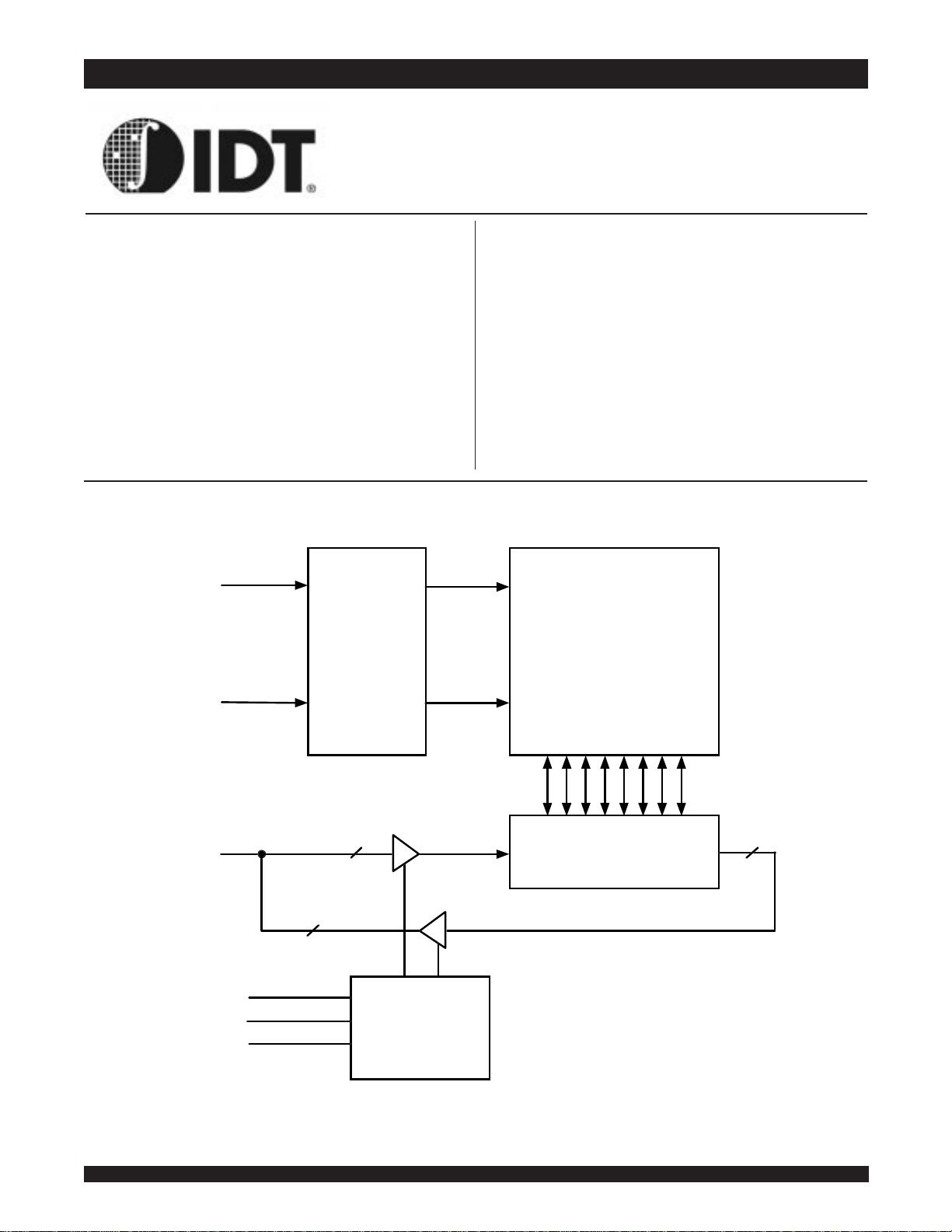
Functional Block Diagram
0
A
•
•
ADDRESS
•
16
A
DECODER
Description
The IDT71V124 is a 1,048,576-bit high-speed static RAM organized
as 128K x 8. It is fabricated using IDT’s high-performance, high-reliability
CMOS technology. This state-of-the-art technology, combined with innovative circuit design techniques, provides a cost-effective solution for highspeed memory needs. The JEDEC center power/GND pinout reduces
noise generation and improves system performance.
The IDT71V124 has an output enable pin which operates as fast as
5ns, with address access times as fast as 9ns available. All bidirectional inputs and outputs of the IDT71V124 are LVTTL-compatible and
operation is from a single 3.3V supply. Fully static asynchronous
circuitry is used; no clocks or refreshes are required for operation.
•
•
•
1,048,576-BIT
MEMORY ARRAY
I/O0-I/O
7
WE
OE
CS
©2003- Integrated Device Technology, Inc.
8
8
I/OCONTROL
.
8
CONTROL
LOGIC
1
3873 drw 01
NOVEMBER 2003
DSC-3873/07
IDT71V124SA, 3.3V CMOS Static RAM
Symbol
Rating
Value
Unit
DD
IN
OUT
A
Commercial
Industrial
BIAS
STG
T
OUT
I/O
OUT
IN
387 3 t b l 01
Symbol
Param ete r
(1)
Conditio ns
Max.
Unit
IN
I/O
OUT
Symbol
Param ete r
Min.
Typ.
Max.
Unit
V
DD
(1)
Supply Voltage
3.15
3.3
3.6VV
DD
(2)
Supply Voltage
3.0
3.3
3.6VVSSGround
000VVIHInput High Voltage
2.0
____
VDD+0.3
(3)
V
VILInput Low Voltage
–0.5
(1)
____
0.8
V
3873 tbl 04
Symb ol
Param et er
Test Conditions
Min.
Max.
Unit
L
I
DD
LO
OUT =
DD
OL
OH
387 3 tb l 0 5
Grade
Temperature
GND
V
DD
1 Meg (128K x 8-Bit) Center Power & Ground Pinout Commercial and Industrial Temperature Ranges
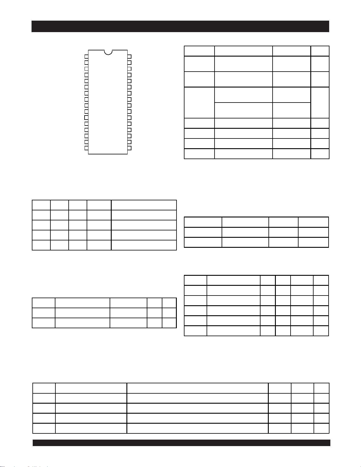
Pin Configuration
A
0
1
A
2
1
3
A
2
4
A
3
CS
DD
WE
A
A
A
A
0
1
2
3
4
5
6
7
5
6
7
8
9
10
11
12
13 20
14 19
15 18
16
I/O
I/O
V
GND
I/O
I/O
SOJ and TSOP
Top View
Truth Table
CS OE WE
LLHDATA
(1)
SO32-2
SO32-3
SO32-4
32
31
30
29
28
27
26
25
24
23
22
21
17
3873 drw 02
Read Dat a
A
16
A
15
A
14
A
13
OE
I/O
7
I/O
6
GND
V
DD
I/O
5
I/O
4
.
A
12
A
11
A
10
A
9
A
8
Function
Absolute Maximum Ratings
V
Supply Voltage Relative
(1)
-0.5 to +4.6 V
to GND
, V
V
Terminal Voltage Relative
-0.5 to VDD+0.5 V
to GND
T
Operating Temperature
Operating Temperature
T
T
P
I
NOTE:
1. Stresses greater than those listed under ABSOLUTE MAXIMUM RATINGS may cause
permanent damage to the device. This is a stress rating only and functional operation
of the device at these or any other conditions above those indicated in the operational
sections of this specification is not implied. Exposure to absolute maximum rating
conditions for extended periods may affect reliabilty.
Temperature Under Bias -55 to +125
Storage Temp erature -55 to + 125
Po we r Dis si p atio n 1. 25 W
DC Outp ut Cu rre nt 50 mA
-0 to + 70
-40 to +85
o
C
o
C
o
C
3873 tbl 02
Recommended Operating Temperature and Supply Voltage
LXLDATA
L H H High-Z Output Disabled
H X X High-Z Deselect ed – S tandby
NOTE:
1. H = VIH, L = VIL, X = Don't care.
Write Dat a
Comme rci al 0°C to +70° C 0V See Be l ow
Industrial -40°C to +85°C 0V See Below
Recommended DC Operating
Conditions
Capacitance
(TA = +25°C, f = 1.0MHz, SOJ package)
C
Input Ca pacitance VIN = 3dV 6 pF
C
I/O Capacitance V
NOTE:
1. This parameter is guaranteed by device characterization, but is not production tested.
= 3dV 7 pF
3873 tbl 0 3
NOTES:
1. For 71V124SA10 only.
2. For all speed grades except 71V124SA10.
3. VIH (max.) = VDD+2V for pulse width less than 5ns, once per cycle.
4. VIL (min.) = –2V for pulse width less than 5ns, once per cycle.
DC Electrical Characteristics
(VDD = Min. to Max., Commercial and Industrial Temperature Ranges)
3873 tbl 02a
|I
| Input Leakage Current VDD = Max., VIN = GND to V
|I
Output Leakage Current VDD = Max.,CS = VIH, V
|
V
Output Low Voltage IOL = 8mA, VDD = Min.
V
Output High Voltage IOH = –4mA, VDD = M in. 2.4
GND to V
2
___
___
___
5µA
5µA
0.4 V
___
V
IDT71V124SA, 3.3V CMOS Static RAM
Symbol
Parameter
71V124S A10
71V124S A12
71V124S A15
71V124S A20
Com 'l
Ind
Com 'l
Ind
Com 'l
Ind
Com 'l
Ind
1 Meg (128K x 8-Bit) Center Power & Ground Pinout Commercial and Industrial Temperature Ranges
DC Electrical Characteristics
(1, 2)
(VDD = Min. to Max., VLC = 0.2V, VHC = VDD 0.2V)
Unit
CC
I
I
SB1
I
NOTES:
1. All values are maximum guaranteed values.
2. All inputs switch between 0.2V (Low) and VDD–0.2V (High).
3. fMAX = 1/tRC (all address inputs are cycling at fMAX); f = 0 means no address input lines are changing.
Dynamic Operating Current
CS <
VLC, Outputs Open, VDD = Max., f = f
SB
Dynami c Stand b y P o we r Sup p ly Current
CS >
VHC, Outputs Open, VDD = Max., f = f
Full Standby Power Supply Current (static)
CS >
VHC, Outputs Open, VDD = Max., f = 0
MAX
MAX
(3)
(3)
(3)
145 150 130 140 100 120 95 115
45 50 40 40 35 40 30 35
10 10 10 10 10 10 10 10
3873 tbl 06
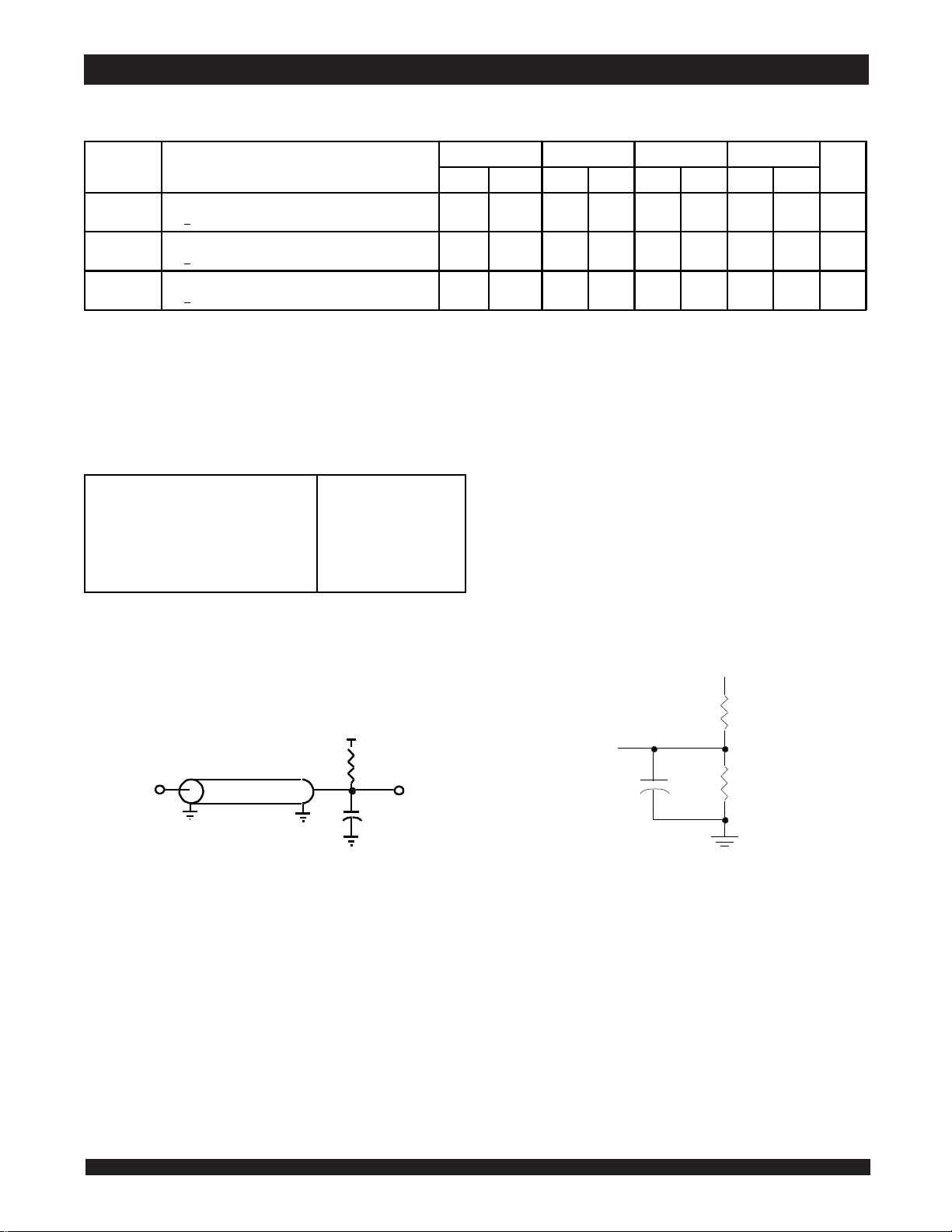
AC Test Conditions
Input P ulse Levels
Input Rise/ Fall Times
Input T iming Refe rence Levels
Output Reference Lev els
AC Test Load
GND to 3. 0V
3ns
1.5V
1.5V
See Figure 1 and 2
3873 tbl 07
mA
mA
mA
I/O
+1.5V
0
=50Ω
Z
Figure 1. AC Test Load
50Ω
30pF
3873 drw03
3.3V
Ω
320
DATA
OUT
350Ω5pF*
.
*Including jig and scope capacitance.
Figure 2. AC Test Load
(for tCLZ, tOLZ, tCHZ, tOHZ , tOW, and tWHZ)
3873 drw 04
6.42
3
 Loading...