

Integrated Device Technology Inc IDT71T024L150PZI, IDT71T024L200PZI Datasheet
Integrated Device Technology, Inc.
LOW POWER 2V CMOS SRAM
1 MEG (128K x 8-BIT)
ADVANCE
INFORMATION
IDT71T024
FEATURES:
• 128K x 8 Organization
• Wide Operating Voltage Range: 1.8V to 2.7V
• Speed Grades: 150ns, 200ns
• Low Operating Power: 11mA (max)
• Low Standby Power: 5µA (max)
• Low-Voltage Data Retention: 1.5V (min)
• Available in 32-pin, 13.4mm x 8mm Type I TSOP package
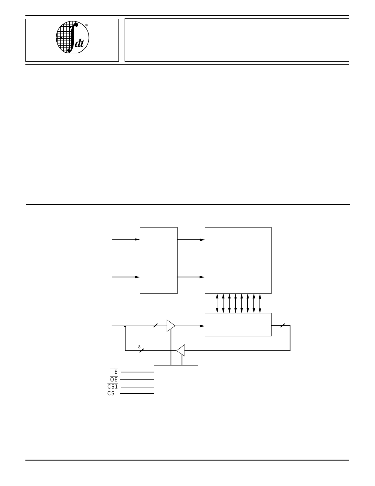
FUNCTIONAL BLOCK DIAGRAM
A0
•
•
•
A16
ADDRESS
DECODER
DESCRIPTION:
The IDT71T024 is a 1,048,576-bit very low-power Static
RAM organized as 128K x 8. It is fabricated using IDT’s highreliability CMOS technology. This state-of-the-art technology,
combined with innovative circuit design techniques, provides
a cost-effective solution for low-power memory needs. It uses
a 6-transistor memory cell.
Operation is from a single extended-range 2.5V supply.
This extended supply range makes the device ideally suited
for unregulated battery-powered applications. Fully static
asynchronous circuitry is used, requiring no clocks or refresh
for operation.
The IDT71T024 is packaged in a JEDEC standard 32-pin
TSOP Type I.
•
•
1,048,576-BIT
MEMORY ARRAY
•
I/O0 – I/O7
The IDT logo is a registered trademark of Integrated Device Technology, Inc.
•
8
WE
OE
CS1
CS2
8
CONTROL
LOGIC
I/O CONTROL
8
3779 drw 01
INDUSTRIAL AND COMMERCIAL TEMPERATURE RANGES MAY 1997
1997 Integrated Device Technology, Inc. DSC-3779/1
1
IDT71T024
LOW POWER 2V CMOS STATIC RAM 1 MEG (128K x 8-BIT) COMMERCIAL AND INDUSTRIAL TEMPERATURE RANGES
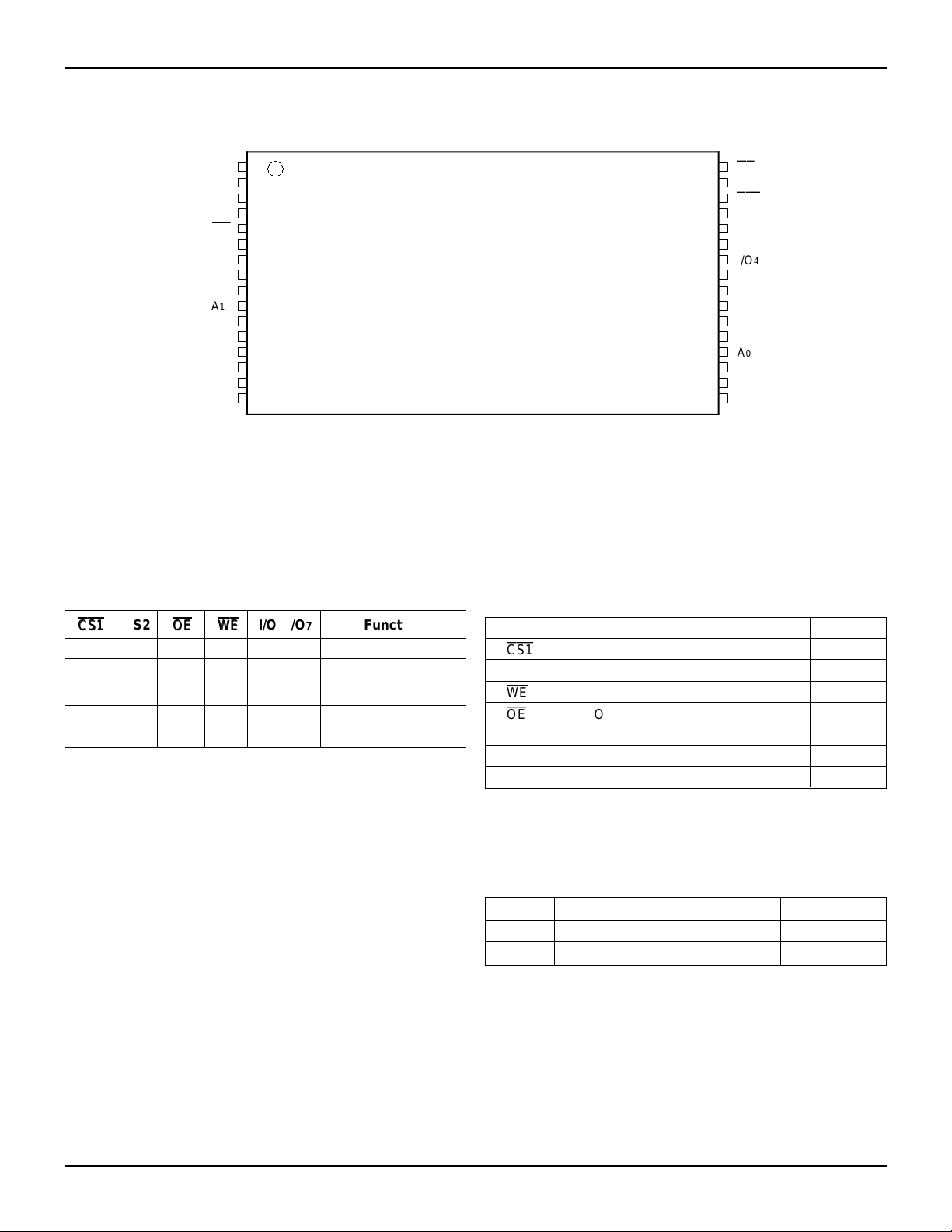
PIN CONFIGURATIONS
11
1
A
A9
2
A8
3
A13
4
5
WE
CS2
6
15
7
A
VDD
8
NC
9
A16
10
A14
11
A12
12
13 20
A7
14 19
A6
15 18
A5
16A4 17
TSOP (I)
TOP VIEW
TRUTH TABLE
CS1
CS2
CS1
(1)
OEOEWEWE I/O0-I/O7 Function
H X X X High-Z Deselected - Standby
X L X X High-Z Deselected - Standby
L H L H DATA
L H X L DATA
OUT Read
IN Write
L H H H High-Z Outputs Disabled
NOTE: 3779 tbl 02
1.H = VIH, L = VIL, X = Don't care.
TSOP
PIN DESCRIPTIONS
A0 – A16 Address Inputs Input
CS1
CS2 Chip Select Input
WE
OE
I/O
0 - I/O7 Data Input/Output I/O
V
DD Power Pwr
V
SS Ground Gnd
OE
32
A10
31
CS1
30
29
28
27
26
25
24
23
22
21
I/O
I/O6
I/O5
I/O4
I/O3
VSS
I/O2
I/O1
I/O0
A0
A1
A2
A3
3779 drw 02
7
Chip Select Input
Write Enable Input
Output Enable Input
3779 tbl 01
CAPACITANCE
(TA = +25°C, f = 1.0MHz)
Symbol Parameter
IN Input Capacitance VIN = 1dV 6 pF
C
I/O I/O Capacitance VOUT = 1dV 7 pF
C
NOTE: 3779 tbl 06
1. This parameter is guaranteed by device characterization, but not prod-
uction tested.
(1)
Conditions Max. Unit
2
IDT71T024
LOW POWER 2V CMOS STATIC RAM 1 MEG (128K x 8-BIT) COMMERCIAL AND INDUSTRIAL TEMPERATURE RANGES
ABSOLUTE MAXIMUM RATINGS
Symbol Rating Com’l. and Ind'l. Unit
(2)
TERM
V
VTERM
TBIAS Temperature Under Bias –55 to +125 °C
STG Storage Temperature –55 to +125 °C
T
P
OUT DC Output Current 20 mA
I
NOTES: 3779 tbl 03
1. Stresses greater than those listed under ABSOLUTE MAXIMUM
RATINGS may cause permanent damage to the device. This is a stress
rating only and functional operation of the device at these or any other
conditions above those indicated in the operational sections of this
specification is not implied. Exposure to absolute maximum rating
conditions for extended periods may affect reliability.
2. V
3. Input, Output,and I/O terminals; 3.6V maximum.
Terminal Voltage with –0.5 to +3.6 V
Respect to V
(3)
Terminal Voltage with –0.5 to VDD+0.5V V
Respect to V
T Power Dissipation 1.0 W
DD terminals only.
SS
SS
(1)
RECOMMENDED OPERATING
TEMPERATURE AND SUPPLY VOLTAGE
Grade Temperature VSS VDD
Commercial 0°C to +70°C 0V 1.8V to 2.7V
Industrial -40°C to +85°C 0V 1.8V to 2.7V
3779 tbl 04
RECOMMENDED DC OPERATING
CONDITIONS
Symbol Parameter Min. Max. Unit
VDD Supply Voltage 1.8 2.7 V
VSS Ground 0 0 V
VIH Input High Voltage VDD x 0.7 VDD + 0.3
V
IL Input Low Voltage –0.3
NOTE: 3779 tbl 05
1. VIH (max.) = VDD + 1.5V for pulse width less than 5ns, once per cycle.
2. V
IL (min.) = –1.5V for pulse width less than 5ns, once per cycle.
(2)
VDD x 0.3 V
(1)
V
DC ELECTRICAL CHARACTERISTICS
VDD = 1.8V to 2.7V, Commercial and Industrial Temperature Ranges
Symbol Parameter Test Conditions Min. Max. Unit
LI| Input Leakage Current VDD = Max., VIN = VSS to VDD —1µA
|I
LO| Output Leakage Current VDD = Max.,
|I
OH Output High Voltage VDD = 1.8 to 2.7V IOH = –0.3mA VDD - 0.2 — V
V
DD = 2.3 to 2.7V IOH = –2mA 1.7 —
V
OL Output Low Voltage VDD = 1.8 to 2.7V IOL = 0.3mA — 0.2 V
V
DD = 2.3 to 2.7V IOL = 2mA — 0.4
V
CS
= VIH, VOUT = VSS to VDD —1µA
3779 tbl 07
DC ELECTRICAL CHARACTERISTICS
(1, 2)
VDD = 1.8 to 2.7V, VLC = 0.2V, VHC = VDD–0.2V, Commercial and Industrial Temperature Ranges
Symbol Parameter Test Conditions Typ.
CC2 Dynamic Operating Current
I
CC Static Operating Current
I
ISB1 Standby Supply Current
CS1
= VLC, CS2 = VHC, Outputs Open, -70 ns — 11 mA
V
DD = 2.7V, f = fMAX
CS1
= VLC, CS2 = VHC, Outputs Open, — 4 mA
WE
= V
HC, VDD = 2.7V, f = 0
CS1
and CS2 = VHC, or CS2 = VLC, -40 to 85°C— 10 µA
Outputs Open, V
(3)
(4)
DD = 2.7V 0 to 70°C— 5
-100 ns — 9
40°C—2
25°C—1
NOTES: 3778 tbl 08
1. All values are maximum guaranteed values.
2. Input low and high voltage levels are 0.2V and V
MAX = 1/tRC (all address inputs are cycling at fMAX).
3. f
4. f = 0 means no address input lines are changing
5. Typical conditions are V
DD = 2.0V and specified temperature.
DD-0.2V respectively for all tests.
.
(5)
Max. Unit
3
 Loading...