


Integrated Device Technology Inc IDT7198L25EB, IDT7198L35DB, IDT7198L35EB, IDT7198L35LB, IDT7198L45DB Datasheet
...
Integrated Device Technology, Inc.
MILITARY TEMPERATURE RANGE MAY 1994
1994 Integrated Device Technology, Inc. 6.4 DSC-1027/4
CMOS STATIC RAMs
64K (16K x 4-BIT)
Added Chip Select and Output Controls
IDT7198S
IDT7198L
FEATURES:
• Fast Output Enable (OE) pin available for added system
flexibility
• Multiple Chip Selects (
CS
1, CS2) simplify system design
and operation
• High speed (equal access and cycle times)
— Military: 20/25/35/45/55/70/85ns (max.)
• Low power consumption
• Battery back-up operation—2V data retention (L version
only)
• 24-pin CERDIP, high-density 28-pin leadless chip carrier,
and 24-pin CERPACK packaging available
• Produced with advanced CMOS technology
• Bidirectional data inputs and outputs
• Inputs/outputs TTL-compatible
• Military product compliant to MIL-STD-883, Class B
DESCRIPTION:
The IDT7198 is a 65,536 bit high-speed static RAM orga-
nized as 16K x 4. It is fabricated using IDT’s high-performance, high-reliability technology—CMOS. This state-of-theart technology, combined with innovative circuit design techniques, provides a cost effective approach for memory intensive applications.
Access times as fast as 20ns are available. The IDT7198
offers a reduced power standby mode, I
SB1, which is activated
when
CS
1 or CS2 goes HIGH. This capability decreases
power, while enhancing system reliability. The low-power
version (L) also offers a battery backup data retention capability where the circuit typically consumes only 30µW when
operating from a 2V battery.
All inputs and outputs are TTL-compatible and operate
from a single 5V supply.
The lDT7198 is packaged in either a 24-pin ceramic DlP,
28-pin leadless chip carrier, and 24-pin CERPACK.
Military grade product is manufactured in compliance with
the latest revision of MIL-STD-883, Class B, making it ideally
suited to military temperature applications demanding the
highest level of performance and reliability.
The IDT logo is a registered trademark of Integrated Device Technology, Inc.
1
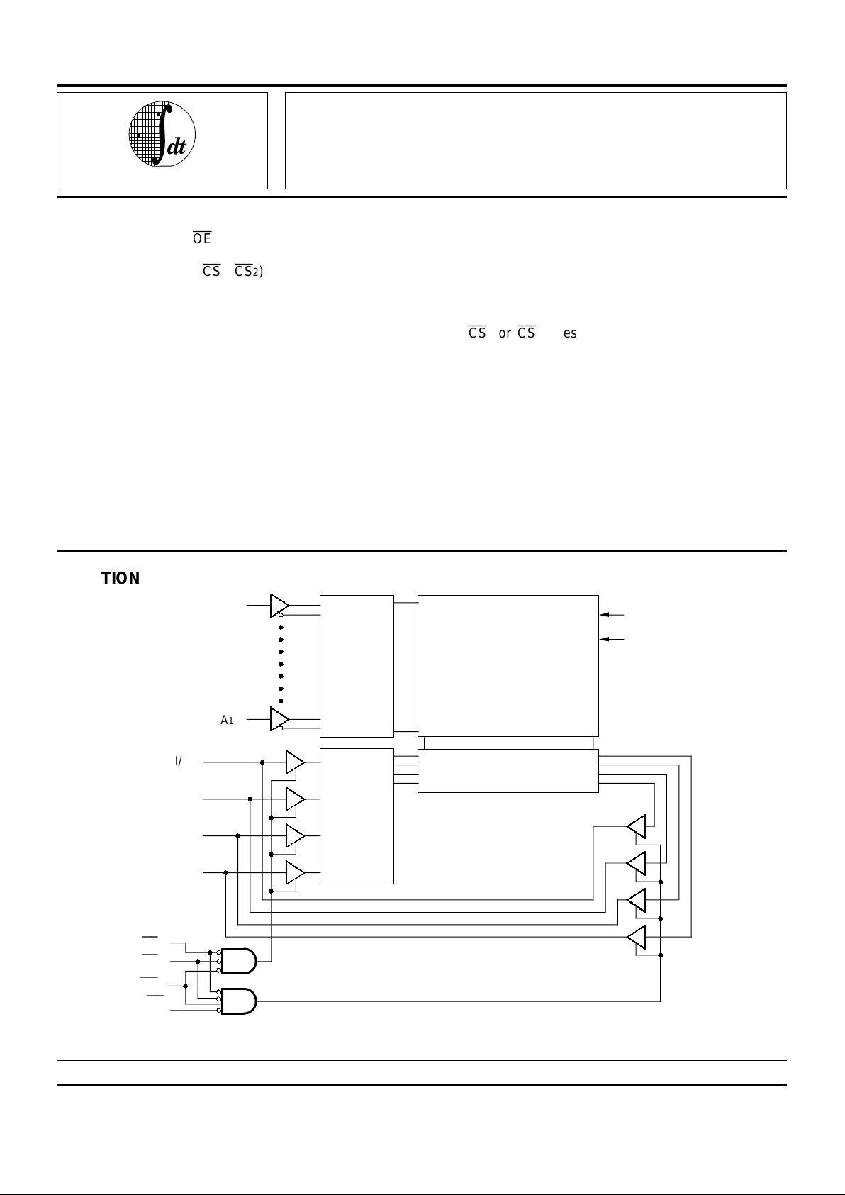
DECODER
65,536-BIT
MEMORY ARRAY
COLUMN I/O
2985 drw 01
INPUT
DATA
CONTROL
GND
A
0
WE
1
CS
1
A
13
I/O
0
I/O
1
I/O
2
I/O
3
V
CC
OE
CS
2
FUNCTIONAL BLOCK DIAGRAM
6.4 2
IDT7198S/L
CMOS STATIC RAM 64K (16K x 4-BIT) Added Chip Select and Output Enable Controls MILITARY TEMPERATURE RANGE
MEMORY CONTROL
The IDT7198 64K high-speed CMOS static RAM incorporates two additional memory control features (an extra chip
select and an output enable pin) which offer additional benefits in many system memory applications.
Both chip selects, Chip Select 1 (
CS
1) and Chip Select 2
(
CS
2), must be LOW to select the memory. If either chip select
is pulled HIGH, the memory will be deselected and remain in
the standby mode. This dual chip select feature (
CS
1, CS2)
also brings the convenience of improved system speeds to the
large memory designer by reducing the external logic required
to perform decoding.
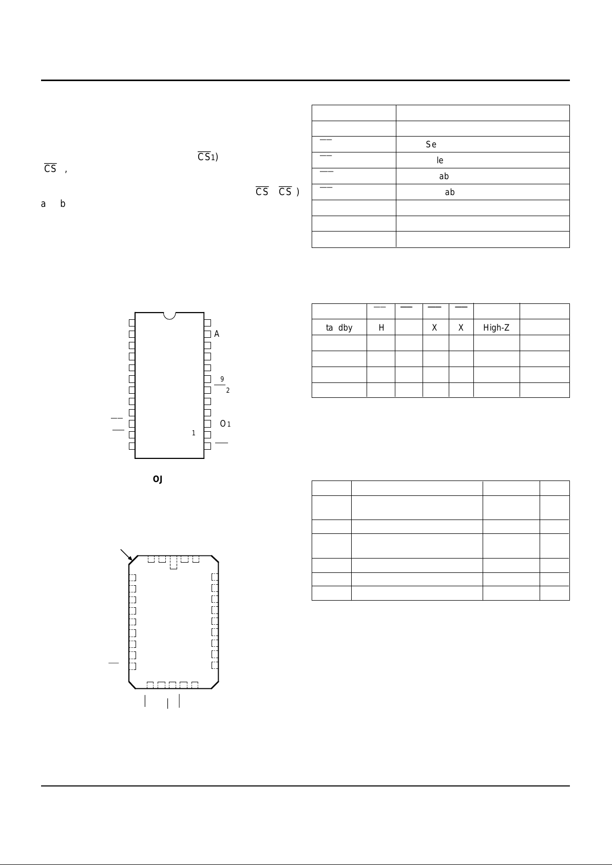
PIN DESCRIPTIONS
Name Description
A0–A13 Address Inputs
CS
1 Chip Select 1
CS
2 Chip Select 2
WE
Write Enable
OE
Output Enable
I/O0–I/O3 Data I/O
VCC Power
GND Ground
2985 tbl 01
TRUTH TABLE
(1)
Mode
CS1CS
CS
2
WEWEOE
OE
I/O Power
Standby H X X X High-Z Standby
Standby X H X X High-Z Standby
Read L L H L DOUT Active
Write L L L X DIN Active
Read L L H H High-Z Active
NOTE: 2985 tbl 02
1. H = VIH, L = VIL, X = don't care.
5
6
7
8
9
10
11
L28-2
26
25
24
23
13 14 15 16 17
32
1
28 27
INDEX
A
5
A
6
A
12
A
11
A
10
CS
12
22
21
A
3
A
4
2985 drw 03
A
7
A
8
20
19
18
A
9
4
1
OE
GND
CS
2
WE
A
2
A
1
A
0
V
CC
NC
NC
NC
A
13
NC
I/O
3
I/O
2
I/O
1
I/O
0
LCC
TOP VIEW
PIN CONFIGURATIONS
2985 drw 02
5
6
7
8
9
10
11
12
A
0
1
2
3
4
24
23
22
21
20
19
18
17
D24-1
E24-1
A
1
A
2
A
3
A
4
A
5
A
6
A
7
A
8
CS
V
CC
WE
A
12
A
11
A
10
16
15
OE
GND
A
9
A
13
1
CS
2
16
15
I/O
3
I/O
2
I/O
1
I/O
0
DIP/SOJ/CERPACK
TOP VIEW
ABSOLUTE MAXIMUM RATINGS
(1)
Symbol Rating Mil. Unit
V
TERM Terminal Voltage –0.5 to +7.0 V
with Respect to GND
T
A Operating Temperature –55 to +125 °C
T
BIAS Temperature –65 to +135 °C
Under Bias
T
STG Storage Temperature –65 to +150 °C
P
T Power Dissipation 1.0 W
I
OUT DC Output Current 50 mA
NOTE: 2985 tbl 03
1. Stresses greater than those listed under ABSOLUTE MAXIMUM
RATINGS may cause permanent damage to the device. This is a stress
rating only and functional operation of the device at these or any other
conditions above those indicated in the operational sections of this
specification is not implied. Exposure to absolute maximum rating conditions for extended periods may affect reliability.
6.4 3
IDT7198S/L
CMOS STATIC RAMS 64K (16K x 4-BIT) Added Chip Select and Output Enable Controls MILITARY TEMPERATURE RANGE
RECOMMENDED DC OPERATING
CONDITIONS
Symbol Parameter Min. Typ. Max. Unit
VCC Supply Voltage 4.5 5.0 5.5 V
GND Supply Voltage 0 0 0 V
VIH Input High Voltage 2.2 — 6.0 V
V
IL Input Low Voltage –0.5
(1)
— 0.8 V
NOTE: 2985 tbl 05
1. VIL (min.) = -3.0V for pulse width less than 20ns, once per cycle.
RECOMMENDED OPERATING
TEMPERATURE AND SUPPLY VOLTAGE
Grade Ambient Temperature GND V CC
Military –55°C to +125°C 0V 5V ± 10%
2985 tbl 06
CAPACITANCE (TA = +25°C, f = 1.0MHz, VCC = 0V)
Symbol Parameter
(1)
Conditions Max. Unit
CIN Input Capacitance VIN = 0V 7 pF
C
I/O I/O Capacitance VOUT = 0V 7 pF
NOTE: 2985 tbl 04
1. This parameter is determined by device characterization, but is not
production tested.
DC ELECTRICAL CHARACTERISTICS
VCC = 5.0V ± 10%, Military Temperature Range Only
IDT7198S IDT7198L
Symbol Parameter Test Condition Min. Max. Min. Max. Unit
|I
LI| Input Leakage Current VCC = Max., — 10 — 5 µA
VIN = GND to VCC
|ILO| Output Leakage Current VCC = Max.,
CS
= VIH, —10 — 5µA
VOUT = GND to VCC
VOL Output Low Voltage IOL = 10mA, VCC = Min. 0.5 — 0.5 V
IOL = 8mA, VCC = Min. — 0.4 — 0.4
V
OH Output High Voltage IOH = –4mA, VCC = Min. 2.4 — 2.4 — V
2985 tbl 07
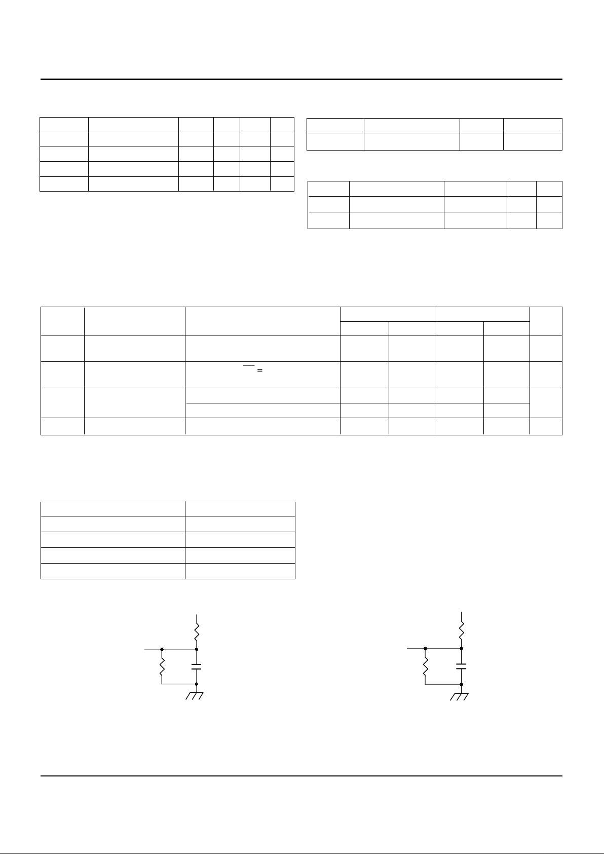
Figure 1. AC Test Load Figure 2. AC Test Load
(for t
CLZ1, 2, tOLZ, tCHZ1, 2, tOHZ, tOW and tWHZ)
*Includes scope and jig capacitances
2985 drw 06
480Ω
5pF*
255Ω
DATA
OUT
5V
2985 drw 05
480Ω
30pF*
255Ω
DATA
OUT
5V
AC TEST CONDITIONS
Input Pulse Levels GND to 3.0V
Input Rise/Fall Times 5ns
Input Timing Reference Levels 1.5V
Output Reference Levels 1.5V
AC Test Load See Figures 1 and 2
2985 tbl 10