

IDT IDT7188S, IDT7188L User Manual
CMOS Static RAM
64K (16K x 4-Bit)
Features
◆◆
◆
◆◆
High-speed (equal access and cycle times)
– Military: 25/35/45/55/70/85ns (max.)
◆◆
◆
◆◆
Low power consumption
◆◆
◆
◆◆
Battery backup operation — 2V data retention
(L version only)
◆◆
◆
◆◆
Available in high-density industry standard 22-pin, 300 mil
ceramic DIP
◆◆
◆
◆◆
Produced with advanced CMOS technology
◆◆
◆
◆◆
Inputs/outputs TTL-compatible
◆◆
◆
◆◆
Military product compliant to MIL-STD-883, Class B
Description
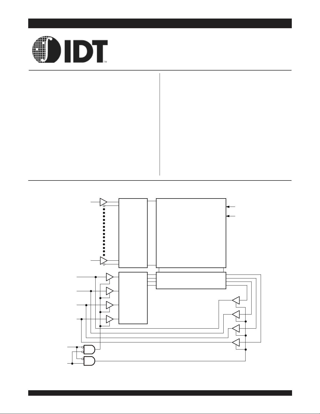
The IDT7188 is a 65,536-bit high-speed static RAM organized as
16K x 4. It is fabricated using IDT’s high-performance, high-reliability
technology — CMOS. This state-of-the-art technology, combined with
Functional Block Diagram
IDT7188S
IDT7188L
innovative circuit design techniques, provides a cost effective approach
for memory intensive applications.
Access times as fast as 25ns are available. The IDT7188 offers a
reduced power standby mode, ISB1, which is activated when CS goes
HIGH. This capability significantly decreases power while enhancing
system reliability. The low-power version (L) version also offers a battery
backup data retention capability where the circuit typically consumes only
30µW operating from a 2V battery.
All inputs and outputs are TTL-compatible and operate from a single
5V supply. The IDT7188 is packaged in a 22-pin, 300 mil ceramic DIP
providing excellent board-level packing densities.
Military grade product is manufactured in compliance with the latest
revision of MIL-STD-883, Class B, making it ideally suited to military
temperature applications demanding the highest level of performance
and reliability.
CS
I/O
I/O
I/O
I/O
0
A
DECODER
13
A
0
1
2
3
INPUT
DATA
CONTROL
65,536-BIT
MEMORY ARRAY
COLUMN I/O
CC
V
GND
,
WE
©2000 Integrated Device Technology, Inc.
2989 drw 01
FEBRUARY 2001
1
DSC-2989/09
IDT7188S/L
Name
Description
13
0
3
CC
Mode
I/O
Power
OUT
IN
Symbol
Rating
Value
Unit
TERM
A
BIAS
STG
T
OUT
Symbol
Parameter
(1)
Conditions
Max.
Uni t
IN
I/O
OUT
Symbol
Parameter
Min.
Typ.
Max.
Uni t
CC
IH
IL
Grade
Temperature
GND
Vcc
CMOS Static RAM 64K (16K x 4-Bit) Military Temperature Range
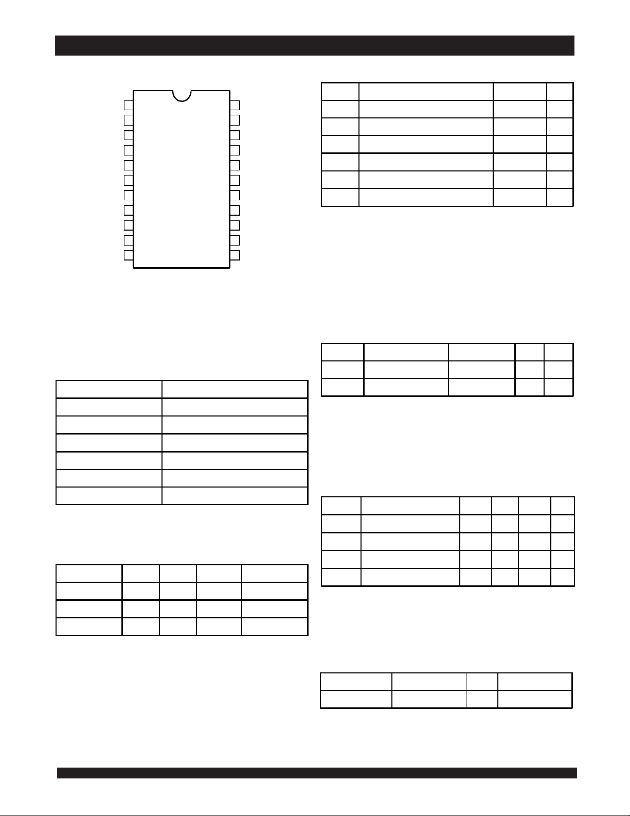
Pin Configuration
Absolute Maximum Ratings
(1)
1
0
A
2
1
A
3
2
A
4
3
A
5
4
A
A
A
A
A
CS
GND
6
5
7
6
8
7
9
8
10
11
Top View
Pin Descriptions
A0 - A
CS
WE
- I/O
I/O
V
GND Ground
D22-1
DIP
22
21
20
19
18
17
16
15
14
13
12
Address Inputs
Chip Se le c t
Write Enabl e
Data Inp ut/ Outp ut
CC
V
13
A
12
A
11
A
10
A
9
A
I/O
I/O
I/O
I/O
WE
2989 drw 02
Power
V
3
2
1
NOTE:
1. Stresses greater than those listed under ABSOLUTE MAXIMUM RATINGS
0
,
Terminal Voltage with Respect to GND -0.5 to +7.0 V
T
Ope rating Tempe rature -55 to + 125oC
T
Temperature Under Bias -65 to +135oC
T
Storage Temperature -65 to +150oC
P
Po we r Di s s ip ati o n 1. 0 W
I
DC Outp ut Cu rre nt 50 mA
2989 tbl 03
may cause permanent damage to the device. This is a stress rating only and
functional operation of the device at these or any other conditions above those
indicated in the operational sections of this specification is not implied. Exposure
to absolute maximum rating conditions for extended periods may affect
reliability.
Capacitance
(TA = +25°C, f = 1.0MHz, VCC = 0V)
C
C
NOTE:
1. This parameter is determined by device characterization, but is not production
tested.
Input Capacitance VIN = 0V 6 pF
I/O Capacitance V
= 0V 6 pF
2989 tbl 04
Recommended DC Operating
Conditions
2989 tbl 01
V
Supp ly Vol tage 4.5 5.0 5.5 V
Truth Table
Standby H X High-Z Standby
Re a d L H D
Write L L D
NOTE:
1. H = VIH, L = VIL , X = don't care.
(1)
CS WE
Active
Active
2989 tbl 02
GND Ground 0 0 0 V
Inp ut Hig h Vo ltag e 2. 2
V
V
Inpu t Lo w Vo l tag e -0. 5
NOTE:
1. VIL (min.) = –3.0V for pulse width less than 20ns,once per cycle.
____
6.0 V
(1)
____
0.8 V
Recommended Operating
Temperature and Supply Voltage
Military -55OC to +1 25OC0V 5V ± 10%
2
2989 tbl 05
2989 tbl 06
IDT7188S/L
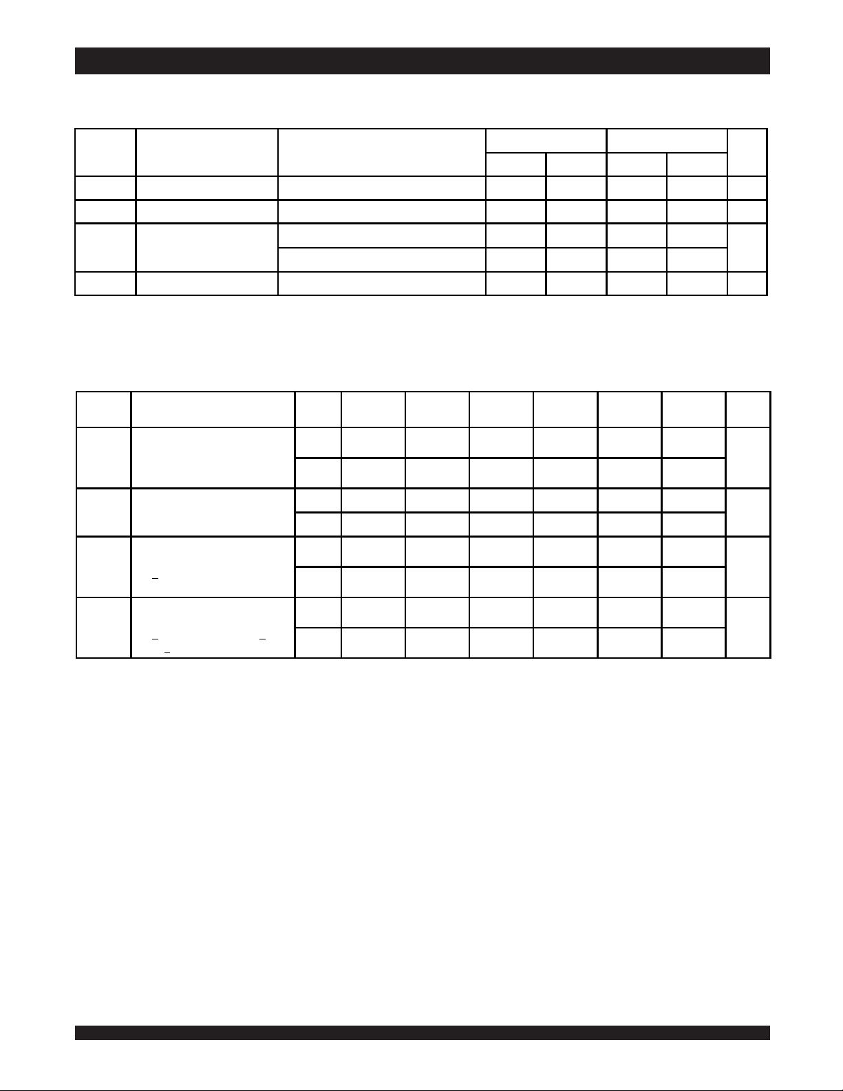
Symbol
Param et e r
Test Conditions
IDT7188S
IDT7188L
Unit
Min.
Max.
Min.
Max.
L
I
CC
OUT
CC
OL
OL
OL
OH
2989 tbl 07
Symbol
Parameter
Power
7188S25
7188L25
7188S35
7188L35
7188S45
7188L45
7188S55
7188L55
7188S70
7188L70
7188S85
7188L85
Uni t
IL
CC
IL
CC
MAX
CC
MAX
HC
2989 tbl 08
CMOS Static RAM 64K (16K x 4-Bit) Military Temperature Range
DC Electrical Characteristics
(VCC = 5.0V ± 10%)
|I
| Inp ut Le a kage Curr e nt VCC = Max., VIN = GND to V
|ILO| Output Leakag e Current VCC = Max., CS = VIH, V
Output Low Voltage
V
V
Outp ut Hig h Vol tag e IOH = -4mA, VCC = Min. 2.4
DC Electrical Characteristics
= 10mA, VCC = Min.
I
I
= 8mA, VCC = Min.
(1)
(VCC = 5V ± 10%, VLC = 0.2V, VHC = VCC - 0.2V)
I
Operating Power
CC1
Supply Current
= V
CS
= Max., f = 0
V
I
Dyna mi c Op e rati ng Curr e nt
CC2
CS = V
= Max., f = f
V
Stand by Po wer Supply
I
SB
Current (TTL Lev el )
VIH, Outp uts Op e n
CS >
= Max., f = f
V
, Outp uts Op e n
(2)
, Outp uts Op e n
(2)
(2)
S 105 105 105 105 105 105
L808080808080
S 155 140 140 140 140 140
L 120 115 110 110 110 105
S605050505050
L404035353535
= GND to V
____
____
____
____
10
10
0.5
0.4
____
____
____
____
____
2.4
5µA
5µA
0.5
V
0.4
____
V
mA
mA
mA
I
Full Standby Power
SB1
Sup p ly Current (CMOS Le ve l )
VHC, VCC = Max., VIN > V
CS >
or VIN < VLC, f = 0
NOTES:
1. All values are maximum guaranteed values.
2. At f = fMAX address and data inputs are cycling at the maximum frequency of read cycles of 1/tRC. f = 0 means no input lines change.
(2)
S202020202020
L 1.5 1.5 1.5 1.5 1.5 1.5
mA
6.42
3
 Loading...