

IDT IDT7133SA-LA, IDT7143SA-LA User Manual

查询IDT7133LA供应商
HIGH SPEED
2K X 16 DUAL-PORT
SRAM
Features
◆◆
◆
◆◆
High-speed access
– Military: 25/35/45/55/70/90ns (max.)
– Industrial: 25/35/55ns (max.)
– Commercial: 20/25/35/45/55/70/90ns (max.)
◆◆
◆
◆◆
Low-power operation
– IDT7133/43SA
Active: 1150mW (typ.)
Standby: 5mW (typ.)
– IDT7133/43LA
Active: 1050mW (typ.)
Standby: 1mW (typ.)
◆◆
◆
◆◆
Versatile control for write: separate write control for lower
and upper byte of each port
◆◆
◆
◆◆
MASTER IDT7133 easily expands data bus width to 32 bits
or more using SLAVE IDT7143
◆◆
◆
◆◆
On-chip port arbitration logic (IDT7133 only)
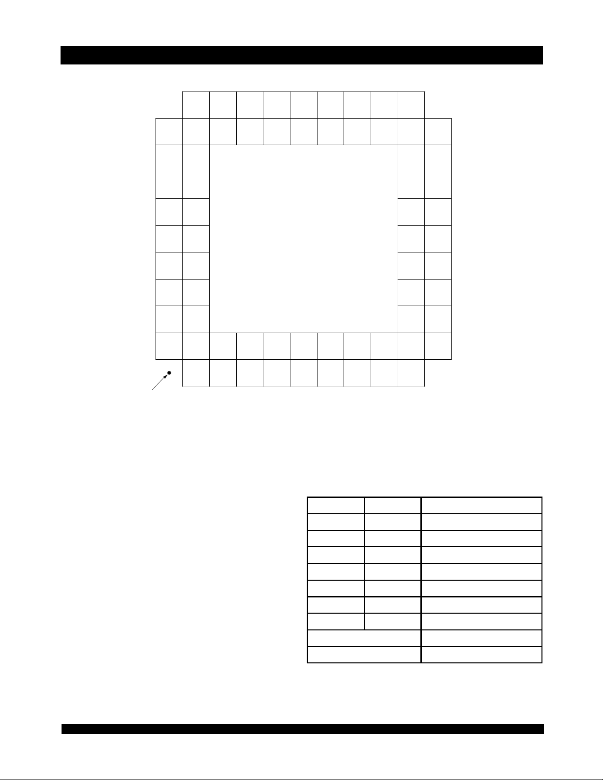
Functional Block Diagram
IDT7133SA/LA
IDT7143SA/LA
◆◆
◆
◆◆
BUSY output flag on IDT7133; BUSY input on IDT7143
◆◆
◆
◆◆
Fully asynchronous operation from either port
◆◆
◆
◆◆
Battery backup operation–2V data retention
◆◆
◆
◆◆
TTL-compatible; single 5V (±10%) power supply
◆◆
◆
◆◆
Available in 68-pin ceramic PGA, Flatpack, PLCC and 100pin TQFP
◆◆
◆
◆◆
Military product compliant to MIL-PRF-38535 QML
◆◆
◆
◆◆
Industrial temperature range (–40°C to +85°C) is available
for selected speeds
Description
The IDT7133/7143 are high-speed 2K x 16 Dual-Port Static RAMs.
The IDT7133 is designed to be used as a stand-alone 16-bit Dual-Port
RAM or as a “MASTER” Dual-Port RAM together with the IDT7143
“SLAVE” Dual-Port in 32-bit-or-more word width systems. Using the
IDT MASTER/SLAVE Dual-Port RAM approach in 32-bit-or-wider
R/
W
LUB
L
CE
R/
W
LLB
OE
L
I/O8L-I/O
I/O0L- I/O
BUSY
15L
7L
(1)
L
A
10L
A
0L
ADDRESS
DECODER
CE
L
CONTROL
11
I/O
MEMORY
ARBITRATION
(IDT7133ONLY)
NOTE:
1. IDT7133 (MASTER): BUSY is open drain output and requires pull-up resistor.
IDT7143 (SLAVE): BUSY is input.
ARRAY
LOGIC
I/O
CONTROL
ADDRESS
DECODER
11
CE
RUB
R/
W
CE
R
R/
W
RLB
OE
R
I/O8R-I/O
I/O0R-I/O
A
A
R
BUSY
10R
0R
2746 drw 01
15R
7R
R
(1)
©2000 Integrated Device Technology, Inc.
JUNE 2000
1
DSC 2746/11

IDT7133SA/LA, IDT7143SA/LA
,
High-Speed 2K x 16 Dual-Port RAM Military, Industrial and Commercial Temperature Ranges
memory system applications results in full-speed, error-free operation
without the need for additional discrete logic.
Both devices provide two independent ports with separate control,
address, and I/O pins that permit independent, asynchronous access
for reads or writes to any location in memory. An automatic power
down feature, controlled by CE, permits the on-chip circuitry of each
port to enter a very low standby power mode.
Fabricated using IDT’s CMOS high-performance technology, these
devices typically operate on only 1,150mW of power. Low-power (LA)
L
L
L
1
2
3
O
O
O
/
/
/
I
I
I
IDT7133/43
J68-1 / F68-1
Top View
R
R
R
3
4
5
1
1
1
O
O
O
/
/
/
I
I
I
(1,2,3)
)
1
L
(
0
C
O
C
/
I
V
(4)
(5)
)
2
B
(
U
D
R
N
W
/
G
R
B
B
U
L
L
L
L
L
L
L
0
W
W
E
1
/
/
A
O
R
R
R
R
B
R
0
9
L
E
1
R
A
O
A
W
/
R
L
9
8
7
A
A
A
60
59
58
57
56
55
54
53
52
51
50
49
48
47
46
45
44
R
8
A
2746 drw 02
R
R
7
6
A
A
Pin Configurations
L
L
L
L
L
4
6
8
5
7
O
O
INDEX
I/O
9L
I/O
10L
I/O
11L
I/O
12L
I/O
13L
14L
I/O
I/O
15L
(1)
V
CC
(2)
GND
I/O
0R
I/O
1R
2R
I/O
I/O
3R
I/O
4R
I/O
5R
I/O
6R
I/O
7R
NOTES:
1. Both V
operation.
2. Both GND pins must be connected to the ground supply to ensure reliable
operation.
3. J68-Package body is approximately 0.95 in x 0.95 in x 0.17 in.
F68-Package body is approximately 1.18 in x 1.18 in x 0.16 in.
PN100-Package body is approximately 14mm x 14mm x 1.4mm.
4. This package code is used to reference the package diagram.
5. This text does not indicate orientation of the actual part-marking.
O
O
O
/
/
/
/
/
I
I
I
I
I
9876543 2168 67 66 65 64 63 62 61
10
11
12
13
14
15
16
17
18
19
20
21
22
23
24
25
26
27 28 29 30 31 32 33 34 35 36 37 38 39 40 41 42 43
R
8
O
/
I
CC pins must be connected to the power supply to ensure reliable
68-Pin PLCC/Flatpack
R
R
R
R
0
2
1
9
1
1
1
O
/
O
O
O
I
/
/
/
I
I
I
versions offer battery backup data retention capability, with each port
typically consuming 200µW for a 2V battery.
The IDT7133/7143 devices have identical pinouts. Each is packed
in a 68-pin ceramic PGA, 68-pin flatpack, 68-pin PLCC and 100-pin
TQFP. Military grade product is manufactured in compliance with the
latest revision of MIL-PRF-38535 QML, making it ideally suited to
military temperature applications demanding the highest level of
performance and reliability.
A
6L
A
5L
A
4L
A
3L
A
2L
1L
A
A
0L
L
BUSY
L
CE
R
CE
R
BUSY
A
0R
A
1R
A
2R
A
3R
A
4R
5R
A
B
B
U
L
Index
I/O
I/O
I/O
I/O
GND
I/O
I/O
GND
I/O
I/O
I/O
I/O
I/O
I/O
I/O
L
L
L
L
L
L
L
L
L
L
D
9
8
7
6
5
4
O
O
/
/
I
I
100999897969594939291908988878685848382818079787776
N/C
1
2
N/C
3
N/C
4
N/C
5
10L
6
11L
7
12L
8
13L
9
10
14L
11
15L
12
CC
V
13
14
0R
1R
15
16
2R
CC
V
17
18
3R
4R
19
20
5R
6R
21
22
N/C
N/C
23
24
N/C
25
N/C
26 27 28 29 30 31 32 33 34 35 36 37 38 39 40 41 42 43 44 45 46 47 48 49 50
R
R
7
8
O
O
/
/
I
I
3
O
O
O
O
O
/
/
/
/
/
I
I
I
I
I
R
R
R
R
R
0
1
2
3
9
1
1
1
1
O
/
O
O
O
O
I
/
/
/
/
I
I
I
I
2
N
O
/
I
G
R
D
4
N
1
G
O
/
I
L
1
0
C
E
C
O
O
/
/
O
V
I
I
IDT7133/43PF
PN100-1
100-Pin TQFP
Top View
B
R
R
D
L
5
E
R
N
1
O
G
O
W
/
/
I
R
L
L
L
C
W
/
E
/
N
C
R
(4)
(5)
R
B
C
/
U
E
R
N
C
W
/
R
L
0
W
/
R
C
/
N
L
C
C
C
/
/
/
1
9
N
N
N
A
A
R
R
R
C
C
/
0
8
/
9
1
A
N
N
A
A
L
L
L
8
7
6
A
A
A
N/C
75
N/C
74
N/C
73
N/C
72
5L
A
71
4L
A
70
3L
A
69
2L
A
68
1L
A
67
0L
A
66
N/C
65
64
63
62
61
60
59
58
57
56
55
54
53
52
51
R
R
7
6
A
A
2746 drw 03
R
5
A
BUSY
GND
N/C
BUSY
N/C
0R
A
1R
A
2R
A
3R
A
4R
A
N/C
N/C
N/C
N/C
L
R
6.42
2
IDT7133SA/LA, IDT7143SA/LA
High-Speed 2K x 16 Dual-Port RAM Military, Industrial and Commercial Temperature Ranges
Pin Configurations
11
10
09
08
07
06
05
04
03
02
01
Pin 1
Designator
NOTES:
1. Both V
CC pins must be connected to the power supply to ensure reliable operation.
(1,2,3)
(con't.)
50 48 46 44 42 40 38 36
51
A
A
I/O
I/O
A
5L
3L
A
4L
12L
11L
2L
5
I/O
13L
6
I/O
14L
A
6L
52 49 47 45 43 41 39 37 3553 34
A
8L
5455
10LA9L
5657
OE
LLB
5859
(1)
W
R/
6061
1L
I/O
6263
I/O
3L
6465
5L
I/O
6667
I/O
7L
168
2
I/O
7L
L
LUB
0L
2L
4L
6L
3
9L
4
10L
A
A
W
R/
V
CC
I/O
I/O
I/O
I/O
I/O8LI/O
BUSY
A
1L
A
0L
IDT7133/43G
GU68-1
68-Pin PGA
Top View
7
9
I/O
15L
8
10
(1)
V
CC
CE
GND
I/O
CE
L
R
BUSY
L
0R
R
(4)
(5)
11
13
)
(2
I/O
1R
12
14
I/O
2R
I/O
A
A
I/O
0R
1R
3R
4R
A
2R
A
3R
15
I/O
5R
16
I/O6RI/O
A
4R
A
5R
32 33
A
8R
30 31
A
10R
28 29
W
R/
RLB
26 27
(2)
GND
24 25
I/O
14R
22 23
I/O
12R
20 21
I/O
10R
18
I/O
8R
17
7R
A
6R
A
7R
A
9R
OE
W
R/
RUB
I/O
I/O
I/O
19
I/O
ABCDEFGHJK L
2746drw 04
R
15R
13R
11R
9R
2. Both GND pins must be connected to the ground supply to ensure reliable operation.
3. Package body is approximately 1.18 in x 1.18 in x 0.16 in.
4. This package code is used to reference the package diagram.
5. This text does not indicate orientation of the actual part-marking.
6.42
3
Pin Names
Left Port Right Port Names
CE
L
W
R/
W
R/
OE
L
A0L - A
0L
I/O
BUSY
LUB
LLB
- I/ O
L
CE
R
W
RUB
R/
W
RLB
R/
OE
R
10L
15L
A0R - A
I/O0R - I/ O
BUSY
CC
V
R
GND Ground
10R
Chip Enabl e
Upp er B y te Re ad/Wri te E nable
Lo wer B yte Re ad/ Write E nab le
Output Enable
Address
15R
Data Inpu t/ Ou tp ut
Busy Flag
Power
2746 tbl 01
IDT7133SA/LA, IDT7143SA/LA
High-Speed 2K x 16 Dual-Port RAM Military, Industrial and Commercial Temperature Ranges
Absolute Maximum Ratings
Symbol Rating Commercial
& Industrial
(2)
TERM
V
Terminal Vo ltage
-0.5 to +7.0 -0.5 to +7.0 V
with Re sp e ct
to GND
T
BIAS
Temperature
-55 to +125 -65 to +135
Under Bias
STG
T
Storage
-65 to +150 -65 to +150
Temperature
(3)
T
P
Power
2.0 2.0 W
Military Unit
(1)
Maximum Operating
Temperature and Supply Voltage
Grade Ambient
Temperature
O
Military -55
o
Commercial 0
C
Industrial -40OC to +85OC0V 5.0V + 10%
o
C
C to + 125OC0V 5.0V + 10%
O
C to +70OC0V5.0V + 10%
NOTES:
1. This is the parameter T
A. This is the "instant on" case temperature.
GND Vcc
Dissipation
OUT
I
DC Outp ut
50 50 mA
Current
NOTES:
27 46 tbl 02
1. Stresses greater than those listed under ABSOLUTE MAXIMUM RATINGS may
cause permanent damage to the device. This is a stress rating only and functional
operation of the device at these or any other conditions above those indicated in
the operational sections of this specification is not implied. Exposure to absolute
maximum rating conditions for extended periods may affect reliability.
TERM must not exceed Vcc + 10% for more than 25% of the cycle time or 10ns
2. V
maximum, and is limited to
< 20mA for the period of VTERM > Vcc + 10%.
Capacitance (TA = +25°C, f = 1.0mhz)
Symbol Parameter
IN
C
Input Cap ac itanc e VIN = 3dV 11 pF
OUT
C
Output Ca pac itanc e V
NOTES:
(1)
Conditions
(2)
Max. Unit
OUT
= 3dV 11 pF
2746 tbl 03
Recommended DC Operating
Conditions
Symbol Parameter Min. Typ. Max. Unit
CC
V
Sup ply Voltag e 4.5 5.0 5.5 V
GND Ground 0 0 0 V
IH
V
Input High Voltage 2.2
IL
V
Input Low Voltag e -0.5
NOTES:
1. VIL (min.) = -1.5V for pulse width less than 10ns.
TERM must not exceed Vcc + 10%.
2. V
____
(1)
____
(2)
6.0
0.8 V
1. This parameter is determined by device characterization but is not production
tested.
2. 3dV references the interpolated capacitance when the input and output switch from
0V to 3V or from 3V to 0V.
(1,2)
2746 tbl 04
V
27 46 tb l 05
DC Electrical Characteristics Over the Operating
Temperature and Supply Voltage Range
Symbol Parameter Test Conditions
|ILI| Input Leak ag e Current
LO
| Output Le akag e Curre nt
|I
OL
V
V
V
Output Lo w Vol tage (I/ O0-I/O15)I
Ope n Drai n Output Lo w Vo ltag e
OL
(
)
BUSY
OH
Output Hig h Vo ltag e IOH = -4mA 2.4
NOTE:
1. At Vcc
< 2.0V, input leakages are undefined.
(1)
VCC = 5. 5V, VIN = 0V to V
IH
OUT
, V
CE
OL
= V
= 4mA
= 0V to V
IOL = 16mA
6.42
(Either port, VCC = 5.0V ± 10%)
CC
CC
4
___
___
___
___
7133SA
7143SA
10
10
0.4
0.5
___
___
___
___
___
2.4
7133LA
7143LA
5µA
5µA
0.4 V
0.5 V
___
UnitMin. Max. Min. Max.
V
2746 tbl 06

IDT7133SA/LA, IDT7143SA/LA
High-Speed 2K x 16 Dual-Port RAM Military, Industrial and Commercial Temperature Ranges
DC Electrical Characteristics Operating
Temperature and Supply Voltage Range
Symbol Parameter Test Conditi on Version Typ.
ICCDyna mi c Op e ra ting
Current
(Both Ports Active)
SB1
Standby Current
I
(Bo th Po rts - TTL
Lev el Inputs )
SB2
Standby Current
I
(One Po rt - TTL
Lev el Inputs )
SB3
Full Standby Current
I
(Bo th Po rts CMO S L e v e l In p uts )
SB4
Full Standby Current
I
(One Po rt CMO S L e v e l In p uts )
IL
, Outputs Disabled
CE = V
(3)
MAX
f = f
L
and CER = V
CE
MAX
f = f
"A"
= VIL and CE
CE
(3)
MAX
f=f
Active Port Outputs Disabled
Both Ports
R
> VCC - 0.2V
CE
IN
> VCC - 0.2V or
V
IN
< 0.2V, f = 0
V
"A"
< 0.2V and
CE
"B"
> VCC - 0.2V
CE
VIN > VCC - 0.2V or VIN < 0.2V
Active Port Outputs Disabled
MAX
f = f
IH
(3)
"B"
IH
= V
L
and
CE
(4)
(5)
(3)
(4)
(2)
(VCC = 5.0V ± 10%)
COM'L SL250
MIL &
IND
S
L
COM'L SL25
MIL &
IND
S
L
COM'L SL140
MIL &
IND
S
L
COM'L SL1.0
MIL &
IND
S
L
COM'L SL140
MIL &
IND
S
L
7133X20
7143X20
Com'l Only
(1)
230
____
____
25
____
____
120
____
____
0.2
____
____
120
____
____
Com'l, Ind
& Military
Max. Typ.
310
250
280
230
____
250
____
230
80
25
70
25
____
25
____
25
200
140
180
100
____
140
____
100
15
1.0
5
0.2
____
1.0
____
0.2
190
140
170
120
____
140
____
120
7133X25
7143X25
(1)
Com'l, Ind
Max. Typ.
300
240
270
210
330
240
300
220
80
25
70
25
90
25
80
25
200
120
170
100
230
120
190
100
15
1.0
4
0.2
30
1.0
10
0.2
190
120
170
100
220
120
200
100
7133X35
7143X35
& Military
(1)
Max. Unit
295
mA
250
325
295
7060mA
75
65
180
mA
160
200
180
mA
15
4
30
10
170
mA
150
190
170
Symbol Parameter Test Condition Versi on Typ.
ICCDyna mi c Op e rati ng
Current
(Bo th Po rts Ac tiv e )
SB1
Stan dby Curre nt
I
(Bo th Po rts - TTL
Lev el Inputs)
SB2
Stan dby Curre nt
I
(One Po rt - TTL
Lev el Inputs)
SB3
Full Standby Current
I
(Bo th Po rts CMOS Lev e l Inp uts)
SB4
I
Full Standby Current
(One Po rt CMOS Lev e l Inp uts)
IL
, Outputs Disabled
CE = V
(3)
MAX
f = f
L
and CER = V
CE
MAX
f = f
"A"
= VIL and CE
CE
MAX
f=f
Active Port Outputs Disabled
Both Ports CEL and
R
> VCC - 0.2V
CE
IN
> VCC - 0.2V or
V
IN
< 0.2V, f = 0
V
"A"
< 0.2V and
CE
"B"
> VCC - 0.2V
CE
VIN > VCC - 0.2V or VIN < 0.2V
Active Port Outputs Disabled
MAX
f = f
IH
(3)
"B"
IH
(3)
(3)
= V
(4)
(5)
(4)
COM'L SL230
MIL &
IND
SL230
COM'L SL25
MIL &
IND
SL25
COM'L SL120
MIL &
IND
SL120
COM'L SL1.0
MIL &
IND
SL1.0
COM'L SL120
MIL &
IND
SL120
NOTES:
CC = 5V, TA = +25°C for Typ., and are not production tested. ICCDC = 180mA (typ.)
1. V
2. 'X' in part number indicates power rating (SA or LA)
3. At f = f
MAX, address and control lines (except Output Enable) are cycling at the maximum frequency read cycle of 1/ tRC, and using “AC Test Conditions" of input levels of
GND to 3V.
4. f = 0 means no address or control lines change. Applies only to inputs at CMOS level standby.
5. Port "A" may be either left or right port. Port "B" is the opposite from port "A".
7133X45
7143X45
Com' l &
Military
(1)
210
210
25
25
100
100
0.2
0.23010
100
100
Com'l, Ind
& Military
Max. Typ.
290
230
250
210
320
230
290
210
75
25
65
25
80
25
70
25
190
120
170
100
210
120
190
100
15
1.0
4
0.2
1.0
0.2
180
120
160
100
200
120
180
100
7133X55
7143X55
(1)
7133X70/90
7143X70/90
Max. Typ.
285
230
250
210
315
230
285
210
70
25
60
25
80
25
70
25
180
120
160
100
210
120
190
100
1541.0
0.2
30
1.0
10
0.2
170
120
150
100
200
120
180
100
Com' l &
Military
(1)
2746 tb l 07a
Max. Unit
280
mA
250
310
280
7060mA
75
65
180
mA
160
200
180
mA
15
4
30
10
170
mA
150
190
170
2746 tbl 07b
6.42
5
 Loading...