

Integrated Device Technology Inc IDT7134LA20C, IDT7134LA20F, IDT7134LA20J, IDT7134LA70J, IDT7134LA70JB Datasheet
...
Integrated Device Technology, Inc.
HIGH-SPEED
4K x 8 DUAL-PORT
STATIC RAM
IDT7134SA/LA
FEATURES:
• High-speed access
— Military: 25/35/45/55/70ns (max.)
— Commercial: 20/25/35/45/55/70ns (max.)
• Low-power operation
— IDT7134SA
Active: 500mW (typ.)
Standby: 5mW (typ.)
— IDT7134LA
Active: 500mW (typ.)
Standby: 1mW (typ.)
• Fully asynchronous operation from either port
• Battery backup operation—2V data retention
• TTL-compatible; single 5V (±10%) power supply
• Available in several popular hermetic and plastic packages
• Military product compliant to MIL-STD-883, Class B
• Industrial temperature range (–40°C to +85°C) is available,
tested to military electrical specifications
DESCRIPTION:
The IDT7134 is a high-speed 4K x 8 Dual-Port Static RAM
designed to be used in systems where on-chip hardware port
arbitration is not needed. This part lends itself to those
systems which cannot tolerate wait states or are designed to
be able to externally arbitrate or withstand contention when
both sides simultaneously access the same Dual-Port RAM
location.
The IDT7134 provides two independent ports with separate
control, address, and I/O pins that permit independent,
asynchronous access for reads or writes to any location in
memory. It is the user’s responsibility to ensure data integrity
when simultaneously accessing the same memory location
from both ports. An automatic power down feature, controlled
by CE, permits the on-chip circuitry of each port to enter a very
low standby power mode.
Fabricated using IDT’s CMOS high-performance
technology, these Dual-Port typically on only 500mW of
power. Low-power (LA) versions offer battery backup data
retention capability, with each port typically consuming 200µW
from a 2V battery.
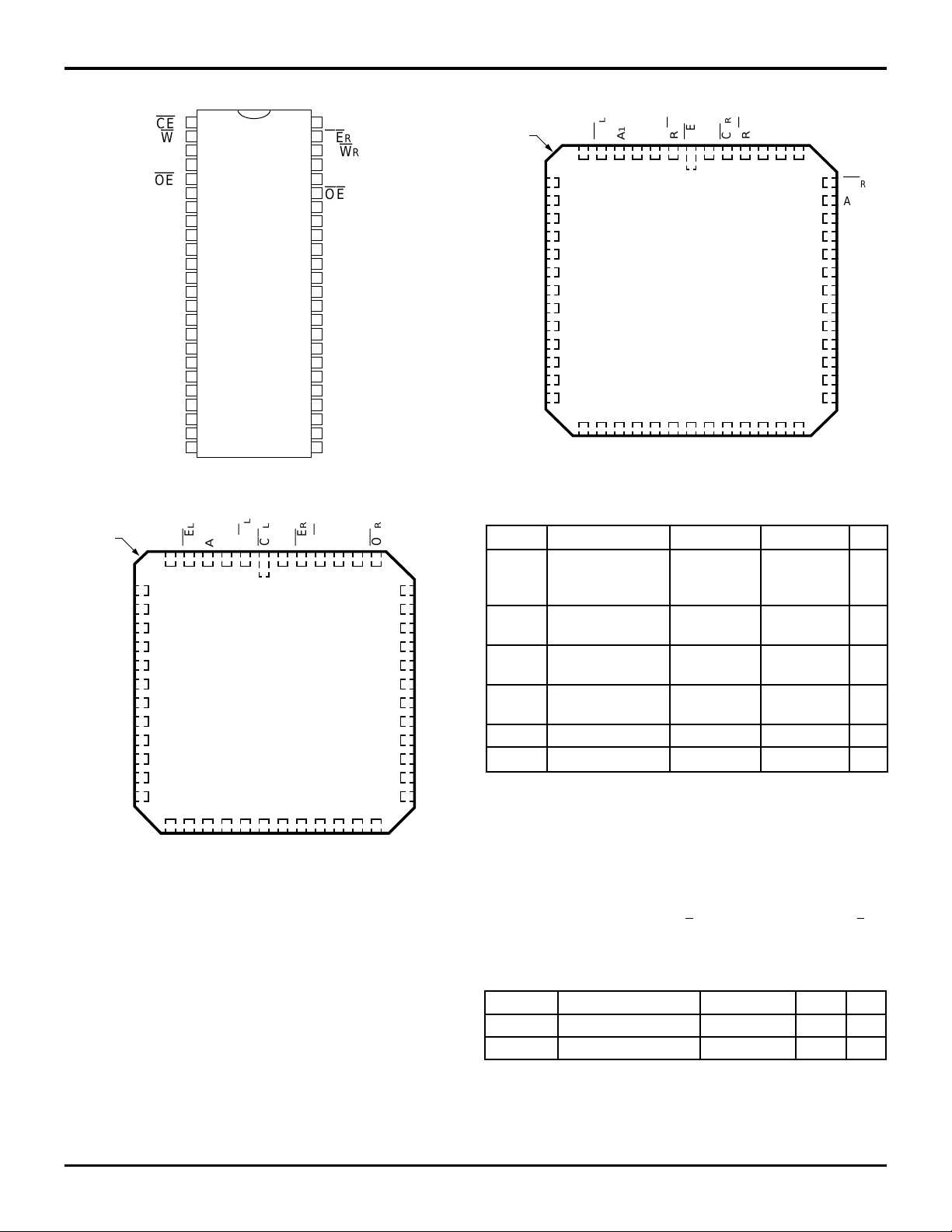
The IDT7134 is packaged on either a sidebraze or plastic
48-pin DIP, 48-pin LCC, 52-pin PLCC and 48-pin Ceramic
Flatpack. Military grade product is manufactured in compliance
with the latest revision of MIL-STD-883, Class B, making it
ideally suited to military temperature applications demanding
the highest level of performance and reliability.
FUNCTIONAL BLOCK DIAGRAM
R/
W
L
CE
L
OE
L
I/O0L- I/O
A0L- A
11L
7L
LEFT SIDE
ADDRESS
DECODE
LOGIC
COLUMN
I/O
MEMORY
ARRAY
COLUMN
I/O
RIGHT SIDE
ADDRESS
DECODE
LOGIC
R/
W
R
CE
R
OE
R
I/O0R- I/O
A0R- A
11R
2720 drw 01
7R
The IDT logo is a registered trademark of Integrated Device Technology, Inc.
MILITARY AND COMMERCIAL TEMPERATURE RANGES OCTOBER 1996
©1996 Integrated Device Technology, Inc. DSC-2720/4
For latest information contact IDT’s web site at www.idt.com or fax-on-demand at 408-492-8391.
6.04
1
IDT7134SA/LA
HIGH-SPEED 4K x 8 DUAL-PORT STATIC RAM MILITARY AND COMMERCIAL TEMPERATURE RANGES
PIN CONFIGURATIONS
148
CE
L
W
A
A
OE
A
A
A
A
A
A
A
A
A
A
11L
10L
0L
1L
2L
3L
4L
5L
6L
7L
8L
9L
2
L
3
4
5
L
6
7
8
9
10
11
12
13
14
15
0L
16
17
1L
18
2L
19
3L
20
4L
21
5L
22
6L
23
7L
24
L
0L
10LA11L
OE
A
A
R/
I/O
I/O
I/O
I/O
I/O
I/O
I/O
I/O
GND
INDEX
(1,2)
IDT7134
P48–1
&
C48–2
DIP
TOP
(3)
VIEW
L
L
W
CE
R/
CC
V
47
46
45
44
43
42
41
40
39
38
37
36
35
34
33
32
31
30
29
28
27
26
25
V
CE
R/
A
A
OE
A
A
A
A
A
A
A
A
A
A
I/O
I/O
I/O
I/O
I/O
I/O
I/O
I/O
2720 drw 02
R
R
W
CE
R/
CC
R
W
11R
10R
R
0R
1R
2R
3R
4R
5R
6R
7R
8R
9R
7R
6R
5R
4R
3R
2R
1R
0R
11RA10R
A
R
R
OE
65432148 47 46 45 44 43
A
I/O
I/O
I/O
1L
7
A
2L
8
A
3L
9
A
4L
10
A
5L
11
A
6L
12
A
7L
13
A
8L
14
A
9L
15
0L
16
1L
17
2L
18
IDT7134
L48-1
&
F48-1
LCC/Flatpack
TOP VIEW
(3)
42
41
40
39
38
37
36
35
34
33
32
31
19 20 21 22 23 25 26 27 28 29 3024
L
5
3L
I/O
4L
I/O
I/O
6L
I/O
7L
I/O
GND
0R
I/O
4R
I/O1RI/O2RI/O3RI/O
5R
I/O
NOTES:
1. All Vcc pins must be connected to the power supply.
2. All GND pins must be connected to the ground supply.
3. This text does not indicate orientation of actual part-marking.
A
0R
A
1R
A
2R
A
3R
A
4R
A
5R
A
6R
A
7R
A
8R
A
9R
I/O
7R
I/O
6R
2720 drw 04
L
W
11L
N/C
R/
A
234567
1
IDT7134
J52-1
PLCC
TOP VIEW (3)
7L
N/C
GND
L
CE
I/O0RI/O1RI/O
INDEX
I/O
I/O
I/O
I/O
L
0L
10L
OE
A
A
8
A
1L
9
A
2L
10
A
3L
11
A
4L
12
A
5L
13
A
6L
14
A
7L
15
A
8L
16
A
9L
17
0L
18
1L
19
2L
20
3L
5L
4L
I/O
I/O
I/O6LI/O
ABSOLUTE MAXIMUM RATINGS
CC
V
R
CE
2R
R
W
N/C
R/
3R
I/O4RI/O5RI/O
I/O
(1)
11R
A
10R
A
474849505152
46
OE
45
44
43
42
41
40
39
38
37
36
35
34
33323130292827262524232221
6R
R
A
0R
A
1R
A
2R
A
3R
A
4R
A
5R
A
6R
A
7R
A
8R
A
9R
N/C
I/O
7R
2720 drw 03
Symbol Rating Com’l. Mil. Unit
(2)
V
TERM
Terminal Voltage –0.5 to +7.0 –0.5 to +7.0 V
with Respect
to Ground
T
A Operating 0 to +70 –55 to +125 °C
Temperature
BIAS Temperature –55 to +125 –65 to +135 °C
T
Under Bias
T
STG Storage –55 to +125 –65 to +150 °C
Temperature
(3)
P
T
Power Dissipation 1.5 1.5 W
I
OUT DC Output Current 50 50 mA
NOTES:
1. Stresses greater than those listed under ABSOLUTE MAXIMUM RATINGS
may cause permanent damage to the device. This is a stress rating only
and functional operation of the device at these or any other conditions
above those indicated in the operational sections of this specification is not
implied. Exposure to absolute maximum rating conditions for extended
periods may affect reliability.
TERM must not exceed Vcc + 0.5V for more than 25%of the cycle time or
2. V
10 ns maximum, and is limited to
< 20mA for the period of VTERM > Vcc
+0.5V.
CAPACITANCE
Symbol Parameter Conditions
C
IN Input Capacitance VIN = 3dv 11 pF
OUT Output Capacitance VOUT = 3dv 11 pF
C
(1)
(TA = +25°C, f = 1.0MHz)
(2)
NOTES:
1. This parameter is determined by device characterization but is not
production tested.
2. 3dv references the interpolated capacitance when the input and output
signals switch from 0V to 3V and from 3V to 0V.
2720 tbl 01
Max. Unit
2720 tbl 02
6.04 2
IDT7134SA/LA
HIGH-SPEED 4K x 8 DUAL-PORT STATIC RAM MILITARY AND COMMERCIAL TEMPERATURE RANGES
RECOMMENDED OPERATING
TEMPERATURE AND SUPPLY VOLTAGE
Ambient
Grade Temperature GND V
Military –55°C to +125°C 0V 5.0V ± 10%
Commercial 0°C to +70°C 0V 5.0V ± 10%
CC
2720 tbl 03
RECOMMENDED DC OPERATING CONDITIONS
Symbol Parameter Min. Typ. Max. Unit
CC Supply Voltage 4.5 5.0 5.5 V
V
GND Ground 0 0 0 V
V
IH Input High Voltage 2.2 — 6.0
V
IL Input Low Voltage –0.5
(1)
— 0.8 V
NOTES: 2720 tbl 04
(2)
V
1. VIL (min.) > –1.5V for pulse width less than 10ns.
TERM must not exceed Vcc + 0.5V.
2. V
DC ELECTRICAL CHARACTERISTICS OVER THE
OPERATING TEMPERATURE AND SUPPLY VOLTAGE
Symbol Parameter Test Conditions Min. Max. Min. Max. Unit
LI| Input Leakage Current
|I
|I
LO| Output Leakage Current
OL Output Low Voltage IOL = 6mA — 0.4 — 0.4 V
V
OH Output High Voltage IOH = –4mA 2.4 — 2.4 — V
V
NOTE: 2720 tbl 05
1. At Vcc ≤ 2.0V input leakages are undefined.
(1)
VCC = 5.5V, VIN = 0V to VCC —10— 5 µA
CE
= VIH, VOUT = 0V to VCC —10— 5µA
OL = 8mA — 0.5 — 0.5 V
I
(VCC = 5V ± 10%)
IDT7134SA IDT7134LA
DC ELECTRICAL CHARACTERISTICS OVER THE
OPERATING TEMPERATURE AND SUPPLY VOLTAGE RANGE
7134X20
Symbol Parameter Test Conditions Version Typ.
I
CC Dynamic Operating
CE
= VIL MIL. S — — 160 310 150 300 140 280 140 270 140 270 mA
Current Outputs Open L — — 160 260 150 250 140 240 140 220 140 220
(Both Ports Active) f = f
MAX
COM’L.S 170 280 160 280 150 260 140 240 140 240 140 240
(3)
L 170 240 160 220 150 210 140 200 140 200 140 200
I
SB1 Standby Current
(Both Ports—TTL f = f
CE
L and CER = VIH MIL. S — — 25 100 25 75 25 70 25 70 25 70 mA
(3)
MAX
L— — 25 8025 5525 50 25 50 2550
Level Inputs) COM’L.S 25 110 25 80 25 75 25 70 25 70 25 70
L2580255025 4525 4025402540
I
SB2 Standby Current
(One Port—TTL
Level Inputs) Active Port Outputs COM’L. S 105 180 95 180 85 170 75 160 75 160 75 160
I
SB3 Full Standby Current Both Ports CEL and MIL. S — — 1.0 30 1.0 30 1.0 30 1.0 30 1.0 30 mA
(Both Ports—All
CMOS Level Inputs) V
I
SB4 Full Standby Current One Port
(One Port—All
CMOS Level Inputs) V
CE
= V
and MIL. S — — 95 210 85 200 75 190 75 180 75 180 mA
"A"
IL
= V
CE
"B"
IH
Open, f = fMAX
R ≥ VCC - 0.2V L — — 0.2 10 0.2 10 0.2 10 0.2 10 0.2 10
CE
IN ≥ VCC - 0.2V or COM’L. S 1.0 15 1.0 15 1.0 15 1.0 15 1.0 15 1.0 15
V
IN ≤ 0.2V, f = 0
≥ VCC - 0.2V L — — 95 150 85 130 75 120 75 120 75 120
CE
"B"
IN ≥ VCC - 0.2V or COM’L. S 105 170 95 170 85 160 75 150 75 150 75 150
IN ≤ 0.2V L 105 130 95 120 85 110 75 100 75 100 75 100
V
Active Port Outputs
Open, f = f
(3)
(3)
CE
or MIL. S — — 95 210 85 190 75 180 75 170 75 170 mA
"A"
(3)
MAX
L — — 95 170 85 160 75 150 75 150 75 150
L 105 150 95 140 85 130 75 130 75 130 75 130
L 0.2 4.5 0.2 4.0 0.2 4.0 0.2 4.0 0.2 4.0 0.2 4.0
NOTES: 2720 tbl 06
1. “X” in part number indicates power rating (SA or LA).
CC = 5V, TA = +25°C for typical, and parameters are not production tested.
2. V
3. f
MAX = 1/tRC = All inputs cycling at f = 1/tRC (except Output Enable). f = 0 means no address or control lines change. Applies only to inputs at CMOS level
standby I
SB3.
4. (Commercial only) 0°C to +70°C temperature range.
(4)
(2)
Max. Typ.
7134X25 7134X35 7134X45 7134X55 7134X70
(2)
Max. Typ.
(1)
(VCC = 5.0V ± 10%)
(2)
Max. Typ.
(2)
Max. Typ.
(2)
Max. Typ.
(2)
Max. Unit
6.04 3
 Loading...