

Integrated Device Technology Inc IDT7005L15PF, IDT7005L17F, IDT7005L17G, IDT7005L17J, IDT7005L17PF Datasheet
...
Integrated Device Technology, Inc.
HIGH-SPEED
8K x 8 DUAL-PORT
STATIC RAM
IDT7005S/L
FEATURES:
• True Dual-Ported memory cells which allow simultaneous access of the same memory location
• High-speed access
— Military: 20/25/35/55/70ns (max.)
— Commercial:15/17/20/25/35/55ns (max.)
• Low-power operation
— IDT7005S
Active: 750mW (typ.)
Standby: 5mW (typ.)
— IDT7005L
Active: 750mW (typ.)
Standby: 1mW (typ.)
• IDT7005 easily expands data bus width to 16 bits or
more using the Master/Slave select when cascading
more than one device
•M/S = H for
M/S = L for
BUSY
output flag on Master,
BUSY
input on Slave
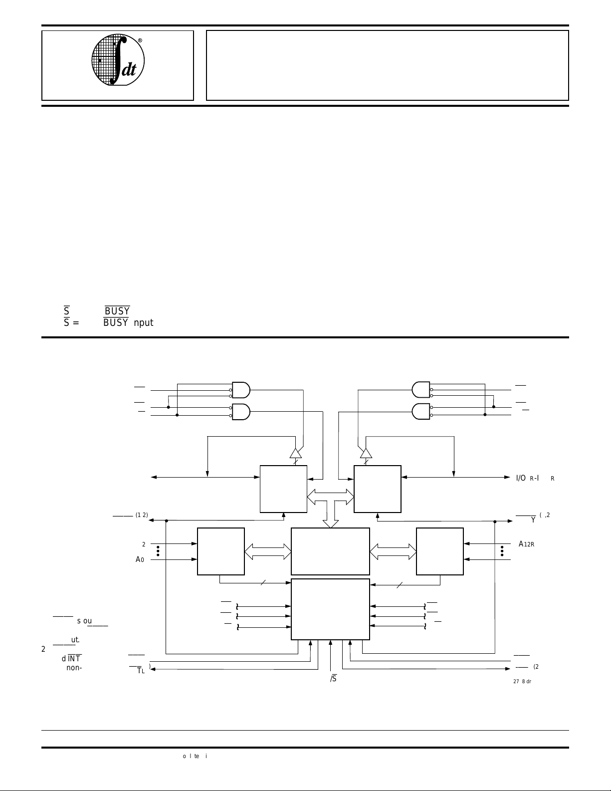
FUNCTIONAL BLOCK DIAGRAM
OE
L
CE
L
L
R/
W
• Busy and Interrupt Flags
• On-chip port arbitration logic
• Full on-chip hardware support of Semaphore signaling
between ports
• Fully asynchronous operation from either port
• Devices are capable of withstanding greater than 2001V
electrostatic discharge
• Battery backup operation—2V data retention
• TTL-compatible, single 5V (±10%) power supply
• Available in 68-pin PGA, 68-pin quad flatpack, 68-pin
PLCC, and a 64-pin TQFP
• Industrial temperature range (–40°C to +85°C) is available, tested to military electrical specifications
DESCRIPTION:
The IDT7005 is a high-speed 8K x 8 Dual-Port Static RAM.
The IDT7005 is designed to be used as a stand-alone DualPort RAM or as a combination MASTER/SLAVE Dual-Port
OE
R
CE
R
R/
W
R
I/O0L- I/O
NOTES:
1. (MASTER):
BUSY
is output;
(SLAVE):
is input.
2.
BUSY
and
are non-tri-stated
push-pull.
The IDT logo is a registered trademark of Integrated Device Technology, Inc.
outputs
INT
BUSY
outputs
7L
(1,2) (1,2)
BUSY
L
A
A
SEM
INT
12L
0L
L
(2)
L
Address
Decoder
CE
OE
R/
W
L
L
L
13
I/O
Control
MEMORY
ARRAY
ARBITRATION
INTERRUPT
SEMAPHORE
LOGIC
M/
S
I/O
Control
Address
Decoder
13
CE
R
OE
R
R/
W
R
I/O0R-I/O
BUSY
A
12R
A
0R
SEM
R
(2)
INT
R
2738 drw 01
7R
R
MILITARY AND COMMERCIAL TEMPERATURE RANGES OCTOBER 1996
©1996 Integrated Device Technology, Inc. DSC-2738/6
For latest information contact IDT’s web site at www.idt.com or fax-on-demand at 408-492-8391.
6.06
1

IDT7005S/L
HIGH-SPEED 8K x 8 DUAL-PORT STATIC RAM MILITARY AND COMMERCIAL TEMPERATURE RANGES
RAM for 16-bit-or-more word systems. Using the IDT MASTER/SLAVE Dual-Port RAM approach in 16-bit or wider
memory system applications results in full-speed, error-free
operation without the need for additional discrete logic.
This device provides two independent ports with separate
control, address, and I/O pins that permit independent,
asynchronous access for reads or writes to any location in
memory. An automatic power down feature controlled by
CE
permits the on-chip circuitry of each port to enter a very low
standby power mode.
Fabricated using IDT’s CMOS high-performance technol-
PIN CONFIGURATIONS
L
L
1L
0L
INDEX
I/O
2L
I/O
3L
I/O
4L
I/O
5L
GND
I/O
6L
I/O
7L
V
CC
GND
0R
I/O
I/O
1R
I/O
2R
V
CC
I/O
3R
I/O
4R
I/O
5R
I/O
6R
I/O
98765432168676665
10
11
12
13
14
15
16
17
18
19
20
21
22
23
24
25
26
27 28 29 30 31 32 33 34 35 36 37 38 39
7R
N/C
I/O
W
OE
N/C
R/
I/O
PLCC / FLATPACK
R
R
R
W
OE
R/
SEM
R
CE
(1,2)
L
L
N/C
CE
N/C
SEM
IDT7005
J68-1
F68-1
TOP VIEW
N/C
N/C
GND
12R
A
CC
V
(3)
11R
A
12L
A
10R
A
10L
11L
A
A
64 63 62 61
40 41 42 43
9R
8R
A
A
6L
7L
8L
9L
A
A
A
A
60
A
5L
59
4L
A
58
A
3L
57
A
2L
56
A
1L
55
A
0L
54
INT
BUSY
GND
M/
BUSY
INT
A
0R
A
1R
A
2R
A
3R
A
4R
2738 drw 02
L
L
S
R
R
53
52
51
50
49
48
47
46
45
44
5R
7R
6R
A
A
A
ogy, these devices typically operate on only 750mW of power.
Low-power (L) versions offer battery backup data retention
capability with typical power consumption of 500µW from a 2V
battery.
The IDT7005 is packaged in a ceramic 68-pin PGA, a 68pin quad flatpack, a 68-pin PLCC and a 64-pin Thin Plastic
Quad Flatpack (TQFP). Military grade product is manufactured in compliance with the latest revision of MIL-STD-883,
Class B, making it ideally suited to military temperature
applications demanding the highest level of performance and
reliability.
L
L
L
0L
INDEX
I/O
I/O
I/O
I/O
GND
I/O
I/O
V
CC
GND
I/O
I/O
I/O
V
CC
I/O
I/O
I/O
1L
I/O
I/O
64
63
62
1
2L
2
3L
3
4L
4
5L
5
6
6L
7
7L
8
9
10
0R
11
1R
12
2R
13
14
3R
15
4R
16
5R
17
181920
OE
W
SEM
R/
61
60
21
L
12L
CC
CE
A
V
N/C
57
58
59
56
IDT7005
PN-64
TQFP
TOP VIEW
24
23
25
22
11L
A
55
26
8L
9L
10L
A
A
54
53
(3)
27
28
5L
6L
7L
A
A
A
A
52
51
49
50
48
A
4L
47
A
3L
46
A
2L
45
A
1L
44
A
0L
43
INT
BUSY
GND
M/
S
BUSY
INT
A
0R
A
1R
A
2R
A
3R
A
4R
L
L
R
R
42
41
40
39
38
37
36
35
34
33
31
29
32
30
NOTES:
1. All Vcc pins must be connected to the power supply.
2. All GND pins must be connected to the ground supply.
3. This text does not indicate orientation of the the actual part-marking.
R
R
6R
I/O
7R
I/O
R
OE
R
W
R/
SEM
CE
N/C
GND
12R
A
11R
A
10R
A
8R
9R
A
A
2738 drw 03
7R
5R
6R
A
A
A
6.06 2
IDT7005S/L
HIGH-SPEED 8K x 8 DUAL-PORT STATIC RAM MILITARY AND COMMERCIAL TEMPERATURE RANGES
PIN CONFIGURATIONS (CON'T.)
11
10
09
08
07
06
05
04
51 50 48 46 44 42 40 38 36
A
4L
A
2L
A
0L
INT
68-PIN PGA
TOP VIEW
53
A
55
A
57
A
59
V
61
N/C
63
SEM
65
OE
7L
9L
11L
CC
A
5L
52
A
6L
47 45 43 41 34
49 39 37
A
3L
A
1L
54
A
8L
56
A
10L
58
A
12L
60
N/C
62
L
CE
L
64
L
R/
W
L
(1,2)
BUSY
L
GND
IDT7005
G68-1
L
BUSY
M/
(3)
S
INT
1R
A
A
R
3R
35
R
A
0R
A
2R
4R
32
A
7R
30
A
9R
28
A
11R
26
GND
24
N/C
22
SEM
A
5R
33
A
6R
31
A
8R
29
A
10R
27
A
12R
25
N/C
23
R
CE
R
A
676866
03
I/O
0L
N/C
02
13579
I/O
1L
I/O
2L
I/O
GND GND
4L
I/O
7L
11 13 15
I/O
246810121416
01
I/O
3L
I/O
5L
I/O
6L
0R
I/O2RI/O3RI/O
I/O
V
CC
ABCDEFGH JKL
INDEX
NOTES:
CC pins must be connected to power supply.
1. All V
2. All GND pins must be connected to ground supply.
3. This text does not indicate oriention of the actual part-marking
1R
V
CC
I/O
PIN NAMES
CE
R/
OE
A
I/O
SEM
INT
BUSY
20
21
R
OE
R/
W
R
18 19
I/O
7R
4R
N/C
17
I/O
5R
6R
2738 drw 04
Left Port Right Port Names
L
W
L R/WR Read/Write Enable
L
0L – A12L A0R – A12R Address
0L – I/O7L I/O0R – I/O7R Data Input/Output
L
L
L
CE
R Chip Enable
OE
R Output Enable
SEM
R Semaphore Enable
INT
R Interrupt Flag
BUSY
R Busy Flag
M/
S
V
CC Power
Master or Slave Select
GND Ground
2738 tbl 01
6.06 3
IDT7005S/L
HIGH-SPEED 8K x 8 DUAL-PORT STATIC RAM MILITARY AND COMMERCIAL TEMPERATURE RANGES
TRUTH TABLE I – NON-CONTENTION READ/WRITE CONTROL
Inputs
CECE
CE
CECE
R/
WW
W
WW
H X X H High-Z Deselected: Power-Down
L L X H DATA
L H L H DATA
X X H X High-Z Outputs Disabled
NOTE:
1. A0L — A12L is not equal to A0R — A12R.
(1)
OEOE
OE
OEOE
SEMSEM
SEM
SEMSEM
Outputs
0-7 Mode
I/O
IN Write to Memory
OUT Read Memory
2738 tbl 02
TRUTH TABLE II – SEMAPHORE READ/WRITE CONTROL
Inputs Outputs
CECE
CE
CECE
H H L L DATA
H
L X X L — Not Allowed
NOTE:
1. There are eight semaphore flags written to via I/O
ABSOLUTE MAXIMUM RATINGS
Symbol Rating Commercial Military Unit
V
TERM
T
A Operating 0 to +70 –55 to +125 °C
BIAS Temperature –55 to +125 –65 to +135 °C
T
T
STG Storage –55 to +125 –65 to +150 °C
OUT DC Output 50 50 mA
I
NOTES: 2738 tbl 04
1. Stresses greater than those listed under ABSOLUTE MAXIMUM
RATINGS may cause permanent damage to the device. This is a stress
rating only and functional operation of the device at these or any other
conditions above those indicated in the operational sections of this
specification is not implied. Exposure to absolute maximum rating
conditions for extended periods may affect reliability.
TERM must not exceed Vcc + 0.5V for more than 25% of the cycle time
2. V
or 10% maximum, and is limited to
+ 0.5V.
WW
R/
W
WW
u
(2)
Terminal Voltage –0.5 to +7.0 –0.5 to +7.0 V
OEOE
SEMSEM
OE
OEOE
SEM
SEMSEM
I/O
X L DATA
0-7 Mode
OUT Read in Semaphore Flag Data 0ut
IN Write I/O0 into Semaphore Flag
0 and read from I/O0 - I/O15. These eight semaphores are addressed by A0 - A2.
(1)
with Respect
to GND
Temperature
Under Bias
Temperature
Current
< 20mA for the period of VTERM > Vcc
RECOMMENDED OPERATING
TEMPERATURE AND SUPPLY VOLTAGE
Grade Temperature GND V
Military –55°C to +125°C 0V 5.0V ± 10%
Commercial 0°C to +70°C 0V 5.0V ± 10%
RECOMMENDED DC OPERATING
CONDITIONS
Symbol Parameter Min. Typ. Max. Unit
CC Supply Voltage 4.5 5.0 5.5 V
V
GND Supply Voltage 0 0 0 V
IH Input High Voltage 2.2 — 6.0
V
V
IL Input Low Voltage –0.5
NOTES: 2738 tbl 06
1. VIL > -1.5V for pulse width less than 10ns.
TERM must not exceed Vcc + 0.5V.
2. V
CAPACITANCE
(TA = +25°C, f = 1.0MHz) TQFP PACKAGE
Symbol Parameter Conditions
IN Input Capacitance VIN = 3dV 9 pF
C
OUT Output VOUT = 3dV 10 pF
C
NOTES: 2738 tbl 07
1. This parameter is determined by device characterization but is not
production tested.
2. 3dv references the interpolated capacitance when the input and output
signals switch from 0V to 3V or from 3V to 0V.
(1)
Capacitance
Ambient
(1)
(1)
— 0.8 V
(2)
2738 tbl 03
CC
2738 tbl 05
(2)
V
Max. Unit
6.06 4
IDT7005S/L
HIGH-SPEED 8K x 8 DUAL-PORT STATIC RAM MILITARY AND COMMERCIAL TEMPERATURE RANGES
DC ELECTRICAL CHARACTERISTICS OVER THE
OPERATING TEMPERATURE AND SUPPLY VOLTAGE RANGE
Symbol Parameter Test Conditions Min. Max. Min. Max. Unit
LI| Input Leakage Current
|I
LO| Output Leakage Current
|I
OL Output Low Voltage IOL = 4mA — 0.4 — 0.4 V
V
OH Output High Voltage IOH = -4mA 2.4 — 2.4 — V
V
NOTE: 2738 tbl 08
1. At Vcc < 2.0V input leakages are undefined.
(1)
VCC = 5.5V, VIN = 0V to VCC —10—5µA
CE
= VIH, VOUT = 0V to VCC —10—5µA
(VCC = 5.0V ± 10%)
IDT7005S IDT7005L
DC ELECTRICAL CHARACTERISTICS OVER THE
(1)
OPERATING TEMPERATURE AND SUPPLY VOLTAGE RANGE
7005X15 7005X17 7005X20 7005X25
Test
Symbol Parameter Condition Version
CC Dynamic Operating
I
Current
(Both Ports Active) f = f
SB1 Standby Current CEL = CER = VIH MIL. S — — — — 20 90 16 80 mA
I
(Both Ports — TTL
Level Inputs f = f
SB2 Standby Current CE"A"=VIL and CE"B"=VIH
I
CE
= VIL, Outputs Open MIL. S — — — — 160 370 155 340 mA
SEM
= V
IH L — — — — 150 320 145 280
(3)
SEM
MAX
R =
MAX
SEM
L = VIH L — — — — 10 70 10 65
(3)
COM.
COM.
(5)
MIL. S — — — — 95 240 90 215 mA
(One Port — TTL Active Port Outputs Open
Level Inputs) f = f
I
SB3 Full Standby Current Both Ports CEL and MIL. S — — — — 1.0 30 1.0 30 mA
(Both Ports — All
CE
CMOS Level Inputs) V
SB4 Full Standby Current
I
(One Port — All
CMOS Level Inputs)
SEM
CE"
CE"
SEM
Active Port Outputs Open,
NOTES: 2738 tbl 09
1. "X" in part numbers indicates power rating (S or L).
CC = 5V, TA = +25°C, and are not production tested. ICC DC = 120mA typ.)
2. V
3. At f = f
4. f = 0 means no address or control lines change.
5. Port "A"may be either left or right port. Port "B" is the port opposite port "A".
MAX, address and I/O'S are cycling at the maximum frequency read cycle of 1/tRC, and using “AC Test Conditions” of input levels of GND to 3V.
(3)
MAX
SEM
R =
SEM
L > VIH L 95 160 95 160 85 150 80 140
R > VCC - 0.2V
IN > VCC - 0.2V or
V
IN < 0.2V, f = 0
R =
SEM
B" < 0.2V and MIL. S — — — — 90 225 85 200 mA
B" > VCC - 0.2v
R =
SEM
V
IN > VCC - 0.2V or
IN < 0.2V
V
(3)
f = f
MAX
(5)
(4)
L > VCC - 0.2V
L > VCC - 0.2V L — — — — 80 200 75 170
COM.
COM.
COM
Com'l. Only Com'l. Only
(2)
Typ.
Max.
S 170 310 170 310 160 290 155 265
L 160 260 160 260 150 240 145 220
S 20 60 20 60 20 60 16 60
L 10 60 10 50 10 50 10 50
L — — — — 85 210 80 180
S 105 190 105 190 95 180 90 170
L — — — — 0.2 10 0.2 10
S 1.0 15 1.0 15 1.0 15 1.0 15
L 0.2 5 0.2 5 0.2 5 0.2 5
.S 100 170 100 170 90 155 85 145
L 90 140 90 140 80 130 75 120
(VCC = 5.0V ± 10%)
(2)
Typ.
Max. Typ.
(2)
Max. Typ.
(2)
Max.
Unit
6.06 5
IDT7005S/L
HIGH-SPEED 8K x 8 DUAL-PORT STATIC RAM MILITARY AND COMMERCIAL TEMPERATURE RANGES
DC ELECTRICAL CHARACTERISTICS OVER THE
OPERATING TEMPERATURE AND SUPPLY VOLTAGE RANGE
Test Mil. Only
Symbol Parameter Condition Version Typ.
CC Dynamic Operating
I
Current
(Both Ports Active) f = f
SB1 Standby Current
I
(Both Ports — TTL
Level Inputs) f = f
SB2 Standby Current
I
(One Port — TTL Active Port Outputs Open L 75 160 75 160 70 160
Level Inputs) f = f
I
SB3 Full Standby Current Both Ports CEL and MIL. S 1.0 30 1.0 30 1.0 30 mA
(Both Ports — All
CMOS Level Inputs) V
I
SB4 Full Standby Current One Port CE"A" < 0.2V MIL. S 80 175 80 175 75 175 mA
(One Port — All
CMOS Level Inputs)
NOTES: 2738 tbl 10
1. "X" in part numbers indicates power rating (S or L).
2. V
CC = 5V, TA = +25°C and are not production tested. ICC DC = 120mA (typ.)
3. At f = f
4. f = 0 means no address or control lines change.
5. Port "A" may be either left or right port. Port "B" is the port opposite port "A".
MAX, address and I/O'S are cycling at the maximum frequency read cycle of 1/tRC, and using “AC Test Conditions” of input levels of GND to 3V.
CE
= VIL, Outputs Open MIL. S 150 300 150 300 140 300 mA
SEM
= V
IH L 140 250 140 250 130 250
(3)
MAX
COM’L. S 150 250 150 250 — —
L 140 210 140 210 — —
CE
L = CER = VIH MIL. S 13 80 13 80 10 80 mA
SEM
R =
SEM
L = VIH L10 65 10651065
(3)
MAX
COM’L. S 13 60 13 60 — —
L10 50 10 50 — —
CE
"A"=VIL and
MAX
SEM
R =
CE
R > VCC - 0.2V L 0.2 10 0.2 10 0.2 10
IN > VCC - 0.2V or COM’L. S 1.0 15 1.0 15 — —
V
IN < 0.2V, f = 0
SEM
R =
CE
"B" > VCC - 0.2V
SEM
R =
IN > VCC - 0.2V or COM’L. S 80 135 80 135 — —
V
V
IN < 0.2V
Active Port Outputs Open, L 70 110 80 110 — —
f = f
MAX
CE
(3)
SEM
L = VIH L 75 130 75 130 — —
(4)
SEM
L > VCC - 0.2V
SEM
L > VCC - 0.2V L 70 150 70 150 65 150
(3)
"B"=VIL
(5)
(5)
MIL. S 85 190 85 190 80 190 mA
COM’L. S 85 155 85 155 — —
L 0.2 5 0.2 5 — —
(1)
(Cont'd.) (VCC = 5.0V ± 10%)
7005X35 7005X55 7005X70
(2)
Max. Typ.
(2)
Max. Typ.
(2)
Max. Unit
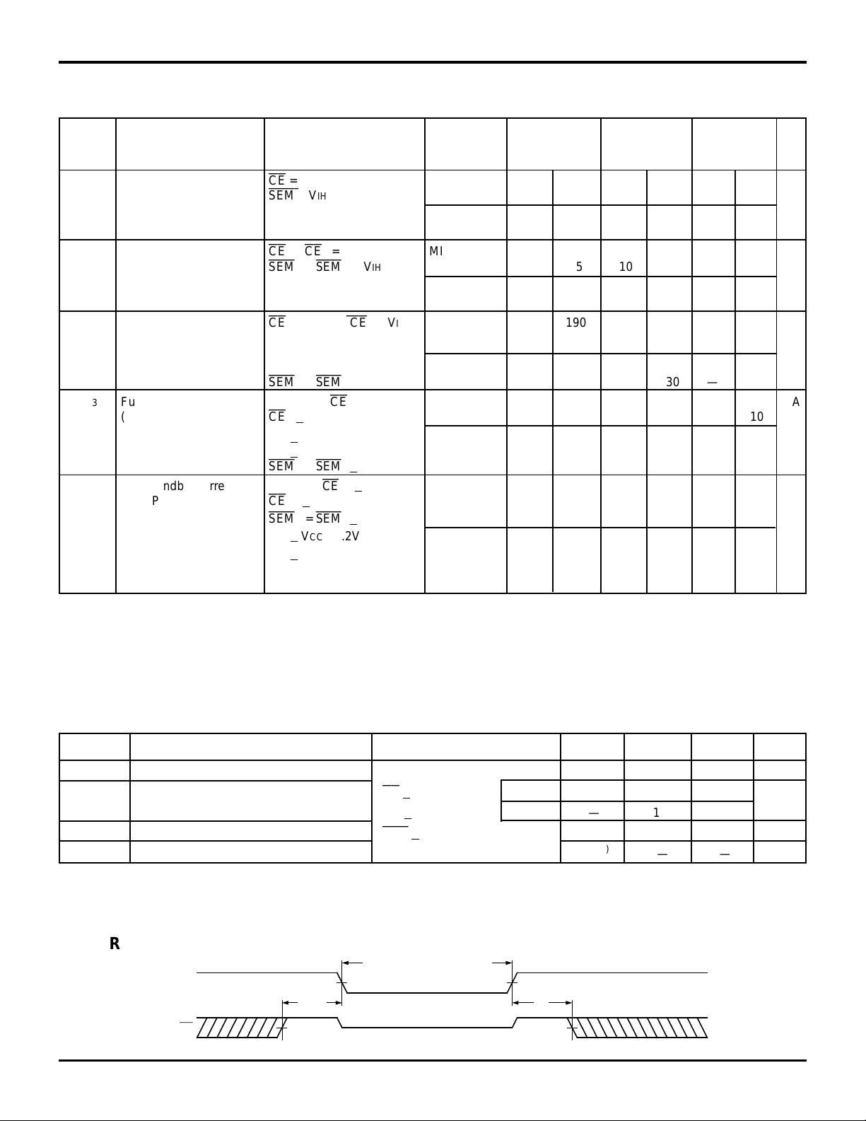
DATA RETENTION CHARACTERISTICS OVER ALL TEMPERATURE RANGES (L Version Only)
(VLC = 0.2V, VHC = VCC - 0.2V)
Symbol Parameter Test Condition Min. Typ.
DR VCC for Data Retention VCC = 2V 2.0 — — V
V
CCDR Data Retention Current
I
(3)
CDR
t
(3)
R
t
NOTES: 2738 tbl 11
1. TA = +25°C, VCC = 2V, and are not production tested.
2. t
RC = Read Cycle Time
3. This parameter is guaranteed by device characteriation, but is not production tested.
Chip Deselect to Data Retention Time
Operation Recovery Time tRC
(4)
(1)
Max. Unit
CE
> VHC MIL. — 100 4000 µA
IN > VHC or ≤ VLC COM’L. — 100 1500
V
SEM
> VHC 0——ns
(2)
——ns
DATA RETENTION WAVEFORM
DATA RETENTION MODE
≥
V
V
CC
CE
4.5V
t
CDR
V
IH
DR
2V
V
DR
6.06 6
4.5V
t
R
V
IH
2738 drw 05
 Loading...