

Integrated Device Technology Inc IDT6167LA100DB, IDT6167LA100PB, IDT6167LA100YB, IDT6167LA20PB, IDT6167LA20Y Datasheet
...
Integrated Device Technology, Inc.
CMOS STATIC RAM
16K (16K x 1-BIT)
IDT6167SA
IDT6167LA
FEATURES:
• High-speed (equal access and cycle time)
— Military: 15/20/25/35/45/55/70/85/100ns (max.)
— Commercial: 15/20/25/35ns (max.)
• Low power consumption
• Battery backup operation — 2V data retention voltage
(IDT6167LA only)
• Available in 20-pin CERDIP and Plastic DIP, and 20-pin
SOJ
• Produced with advanced CMOS high-performance
technology
• CMOS process virtually eliminates alpha particle softerror rates
• Separate data input and output
• Military product compliant to MIL-STD-883, Class B
DESCRIPTION:
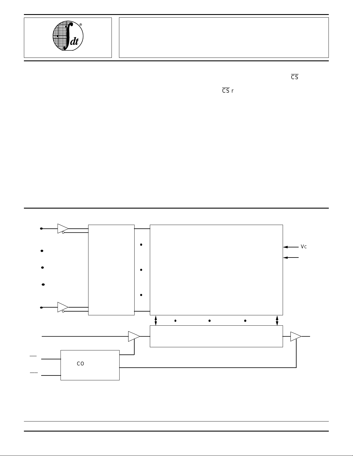
The lDT6167 is a 16,384-bit high-speed static RAM organized as 16K x 1. The part is fabricated using IDT’s highperformance, high reliability CMOS technology.
FUNCTIONAL BLOCK DIAGRAM
A0
Access times as fast as 15ns are available. The circuit also
offers a reduced power standby mode. When CS goes HIGH,
the circuit will automatically go to, and remain in, a standby
mode as long as CS remains HIGH. This capability provides
significant system-level power and cooling savings. The lowpower (LA) version also offers a battery backup data retention
capability where the circuit typically consumes only 1µW
operating off a 2V battery.
All inputs and the output of the IDT6167 are TTL-compatible and operate from a single 5V supply, thus simplifying
system designs.
The IDT6167 is packaged in a space-saving 20-pin, 300 mil
Plastic DIP or CERDIP, Plastic 20-pin SOJ, providing high
board-level packing densities.
Military grade product is manufactured in compliance with
the latest revision of MIL-STD-883, Class B, making it ideally
suited to military temperature applications demanding the
highest level of performance and reliability.
A13
DIN
CS
WE
CONTROL
LOGIC
ADDRESS
DECODE
16,384-BIT
MEMORY ARRAY
I/O CONTROL
VCC
GND
DOUT
2981 drw 01
The IDT logo is a registered trademark of Integrated Device Technology, Inc.
MILITARY AND COMMERCIAL TEMPERATURE RANGES MARCH 1996
1996 Integrated Device Technology, Inc. 2981/5
For latest information contact IDT's web site at www.idt.com or fax-on-demand at 408-492-8391.
5.2
1
IDT6167SA/LA
CMOS STATIC RAM 16K (16K x 1-BIT) MILITARY AND COMMERCIAL TEMPERATURE RANGES
PIN CONFIGURATIONS
V
20
19
18
17
16
15
14
13
12
11
CC
13
A
A
12
11
A
A
10
9
A
A
8
A
7
D
IN
CS
2981 drw 02
D
OUT
WE
GND
0
A
1
A
1
2
A
2
3
A
3
A
4
A
5
A
6
P20-1,
4
D20-1,
5
6
&
S020-1
7
8
9
10
DIP/SOJ
TOP VIEW
PIN DESCRIPTIONS
A0–A13 Address Inputs
CS
WE
Chip Select
Write Enable
VCC Power
DIN DATAIN
DOUT DATAOUT
GND Ground
2981 tbl 01
TRUTH TABLE
Mode
(1)
CSCSWE
WE
Output Power
Standby H X High-Z Standby
Read L H DATAOUT Active
Write L L High-Z Active
NOTE: 2981 tbl 02
1. H = VIH, L = VIL, X = Don't Care.
RECOMMENDED OPERATING
TEMPERATURE AND SUPPLY VOLTAGE
Grade Temperature GND VCC
Military –55°C to +125°C 0V 5V ± 10%
Commercial 0°C to +70°C 0V 5V ± 10%
2981 tbl 06
ABSOLUTE MAXIMUM RATINGS
(1)
Symbol Rating Com’l. Mil. Unit
V
TERM Terminal Voltage –0.5 to +7.0 –0.5 to +7.0 V
with Respect
to GND
A Operating 0 to +70 –55 to +125 °C
T
Temperature
BIAS Temperature –55 to +125 –65 to +135 °C
T
Under Bias
STG Storage –55 to +125 –65 to +150 °C
T
Temperature
PT Power Dissipation 1.0 1.0 W
OUT DC Output 50 50 mA
I
Current
NOTE: 2981 tbl 03
1. Stresses greater than those listed under ABSOLUTE MAXIMUM
RATINGS may cause permanent damage to the device. This is a stress
rating only and functional operation of the device at these or any other
conditions above those indicated in the operational sections of this
specification is not implied. Exposure to absolute maximum rating
conditions for extended periods may affect reliability.
CAPACITANCE (TA = +25°C, f = 1.0MHz)
Symbol Parameter
CIN Input Capacitance VIN = 0V 7 pF
OUT Output Capacitance VOUT = 0V 7 pF
C
NOTE: 2981 tbl 04
1. This parameter is determined by device characterization, but is not
production tested.
(1)
Conditions Max. Unit
RECOMMENDED DC OPERATING
CONDITIONS
Symbol Parameter Min. Typ. Max. Unit
VCC Supply Voltage 4.5 5.0 5.5 V
GND Supply Voltage 0 0 0 V
VIH Input High Voltage 2.2 — 6.0 V
IL Input Low Voltage –0.5
V
NOTE: 2981 tbl 05
1. VIL (min.) = –3.0V for pulse width less than 20ns, once per cycle.
(1)
— 0.8 V
5.2 2
IDT6167SA/LA
CMOS STATIC RAM 16K (16K x 1-BIT) MILITARY AND COMMERCIAL TEMPERATURE RANGES
DC ELECTRICAL CHARACTERISTICS
(1)
(VCC = 5.0V ± 10%, VLC = 0.2V, VHC = VCC – 0.2V)
6167SA/LA15 6167SA/LA20 6167SA/LA25
Symbol Parameter Power Com’l. Mil. Com’l. Mil. Com’l. Mil. Unit
I
CC1 Operating Power Supply Current SA 90 90 90 90 90 90 mA
CS
≤ V
IL, Outputs Open,
VCC = Max., f = 0
CC2 Dynamic Operating Current SA 120 130 100 110 100 100 mA
I
CS
≤ V
IL, Outputs Open,
VCC = Max., f = fMAX
SB Standby Power Supply Current SA 50 50 35 35 35 35 mA
I
(3)
(3)
LA 55 60 55 60 55 60
LA 100 110 80 85 70 75
(TTL Level)
CS
≥ V
IH, Outputs Open, LA 35 35 30 30 25 25
VCC = Max., f = fMAX
(3)
ISB1 Full Standby Power Supply Current SA 5 10 5 10 5 10 mA
(CMOS Level)
CS
≥ V
HC, VCC = Max. LA 0.9 2 0.05 2 0.05 0.9
V
IN ≥ VHC or VIN ≤ VLC, f = 0
DC ELECTRICAL CHARACTERISTICS
(3)
(1)
(CONTINUED)
(VCC = 5.0V ± 10%, VLC = 0.2V, VHC = VCC – 0.2V)
6167SA/LA35 6167SA/LA45
(2)
6167SA/LA55
Symbol Parameter Power Com’l. Mil. Com’l. Mil. Com’l. Mil. Com’l. Mil. Unit
CC1 Operating Power Supply Current SA 90 90 — 90 — 90 — 90 mA
I
CS
≤ V
IL, Outputs Open,
VCC = Max., f = 0
CC2 Dynamic Operating Current SA 100 100 — 100 — 100 — 100 mA
I
CS
≤ V
IL, Outputs Open,
VCC = Max., f = fMAX
SB Standby Power Supply Current SA 35 35 — 35 — 35 — 35 mA
I
(3)
(3)
LA 55 60 — 60 — 60 — 60
LA 65 70 — 65 — 60 — 60
(TTL Level)
CS
≥ V
IH, Outputs Open, LA 20 20 — 20 — 20 — 15
VCC = Max., f = fMAX
(3)
ISB1 Full Standby Power Supply Current SA 5 10 — 10 — 10 — 10 mA
(CMOS Level)
CS
≥ V
HC, VCC = Max. LA 0.05 0.9 — 0.9 — 0.9 — 0.9
V
IN ≥ VHC or VIN ≤ VLC, f = 0
NOTES: 2981 tbl 07
1. All values are maximum guaranteed values.
2. –55°C to +125°C temperature range only. Also available; 85ns and 100ns Military devices.
3. f
MAX = 1/tRC, only address inputs cycling at fMAX. f = 0 means no Address inputs change.
(3)
(2)
6167SA/LA70
(2)
5.2 3
 Loading...