查询IDT2309NZ供应商
IDT2309NZ
NINE OUTPUT 3.3V CLOCK BUFFER
COMMERCIAL AND INDUSTRIAL TEMPERATURE RANGES
NINE OUTPUT
3.3V CLOCK BUFFER
FEA TURES:
• One input to nine output buffer/driver
• Supports two DIMMs or four SO-DIMMs with one additional
output for feedback to an external or chipset PLL
• Low power consumption for mobile applications: less than
32mA at 66.6MHz with unloaded outputs
• 8.7ns input-output delay
• Buffers all frequencies from DC to 133.33MHz
• Output-output skew < 250ps
• Multiple VDD and VSS pins for noise and EMI reduction
• 3.3V operation
• High drive capability
• Available in SOIC and TSSOP packages
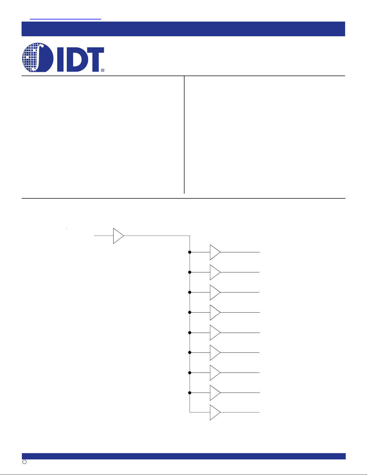
FUNCTIONAL BLOCK DIAGRAM
IDT2309NZ
ADVANCE
INFORMATION
DESCRIPTION:
The IDT2309NZ is a low-cost buffer designed to distribute high-speed
clocks in mobile PC systems and desktop PC systems with SDRAM
support. This part has nine outputs, eight of which can be used to drive
two DIMMs or four SO-DIMMs, and the remaining can be used for external
feedback to a PLL. The IDT2309NZ operates at 3.3V and outputs can run
up to 133.33MHz
The IDT2309NZ is designed for low EMI and power optimization. It has
multiple VDD and VSS pins for noise optimization and consumes less than
32mA at 66.6MHz, making it ideal for the low power requirements of mobile
systems.
BUF_IN
OUTPUT1
OUTPUT2
OUTPUT3
OUTPUT4
OUTPUT5
OUTPUT6
OUTPUT7
OUTPUT8
The IDT logo is a registered trademark of Integrated Device Technology, Inc.
COMMERCIAL AND INDUSTRIAL TEMPERATURE RANGES
2003 Integrated Device Technology, Inc. DSC 6189/6c
1
OUTPUT9
FEBRUARY 2003

IDT2309NZ
NINE OUTPUT 3.3V CLOCK BUFFER
COMMERCIAL AND INDUSTRIAL TEMPERATURE RANGES
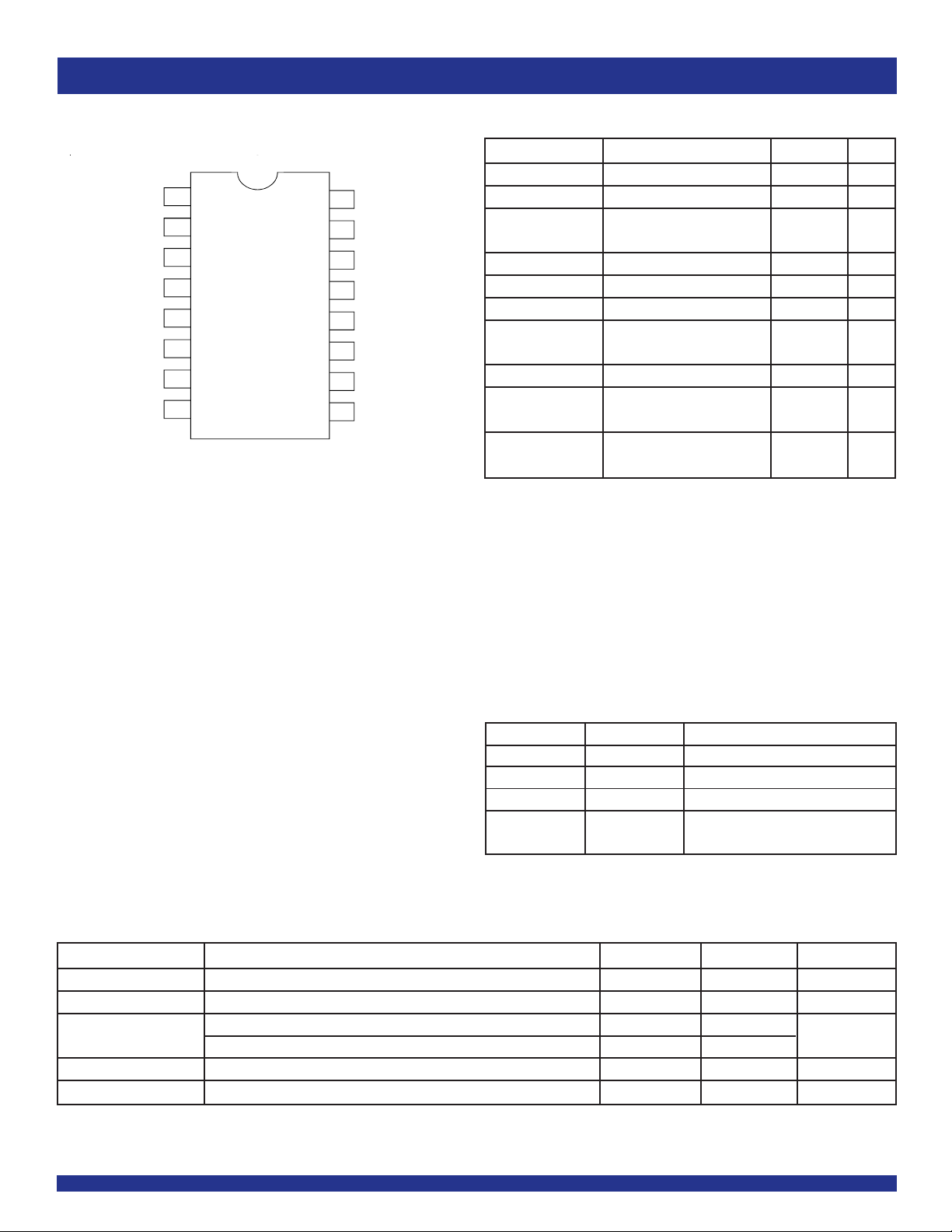
PIN CONFIGURATION
BUF_IN
OUTPUT1
OUTPUT2
VDD
GND
OUTPUT3
OUTPUT4
DD
V
2
3
4
5
6
7
8
SOIC/ TSSOP
TOP VIEW
161
15
14
13
12
11
10
ABSOLUTE MAXIMUM RATINGS
Symbol Rating Max. Unit
VDD Supply Voltage Range –0.5 to +4.6 V
(2)
OUTPUT9
VI
I Input Voltage Range –0.5 to V
V
OUTPUT8
OUTPUT7
DD
V
GND
OUTPUT6
OUTPUT5
9
GND
IIK (VI < 0) Input Clamp Current –50 mA
IO (VO = 0 to VDD) Continuous Output Current ±50 mA
VDD or GND Continuous Current ±100 mA
A = 55°C Maximum Power Dissipation 0.7 W
T
(in still air)
TSTG Storage Temperature Range –65 to +150 °C
Operating Commercial Temperature 0 to +70 °C
Temperature Range
Operating Industrial Temperature -40 to +85 °C
Temperature Range
NOTES:
1. Stresses greater than those listed under ABSOLUTE MAXIMUM RATINGS may cause
2. The input and output negative-voltage ratings may be exceeded if the input and output
3. The maximum package power dissipation is calculated using a junction temperature
(3)
permanent damage to the device. This is a stress rating only and functional operation
of the device at these or any other conditions above those indicated in the operational
sections of this specification is not implied. Exposure to absolute maximum rating
conditions for extended periods may affect reliability.
clamp-current ratings are observed.
of 150°C and a board trace length of 750 mils.
Input Voltage Range (REF) –0.5 to +5.5 V
(except REF) VDD+0.5
(1)
PIN DESCRIPTION
Pin Name Pin Number Functional Description
VDD 4, 8, 13 3.3V Digital Voltage Supply
GND 5, 9, 12 Ground
BUF_IN 1 Input clock
OUTPUT
[1:9] 2, 3, 6, 7, 10 Outputs
11, 14, 15, 16
OPERATING CONDITIONS - COMMERCIAL
Symbol Parameter Min. Max. Unit
VDD Supply Voltage 3 3.6 V
TA Operating Temperature (Ambient Temperature) 0 70 °C
CL Load Capacitance, FOUT < 100MHz — 3 0 pF
Load Capacitance 100MHz < FOUT < 133.33MHz — 15
CIN Input Capacitance — 7 pF
BUF_IN, SDRAM[1:9] Operating Frequency DC 133.33 MHz
2
 Loading...