

Page 1
PRELIMINARY DATASHEET
48 MHZ USB CLOCK SOURCE ICS5OSK482
Description
The ICS5OSK482 is a low cost integrated clock synthesizer
solution designed for replacing crystals and crystal
oscillators.
The ICS5OSK482 generates a very accurate 48.00 MHz
clock output.
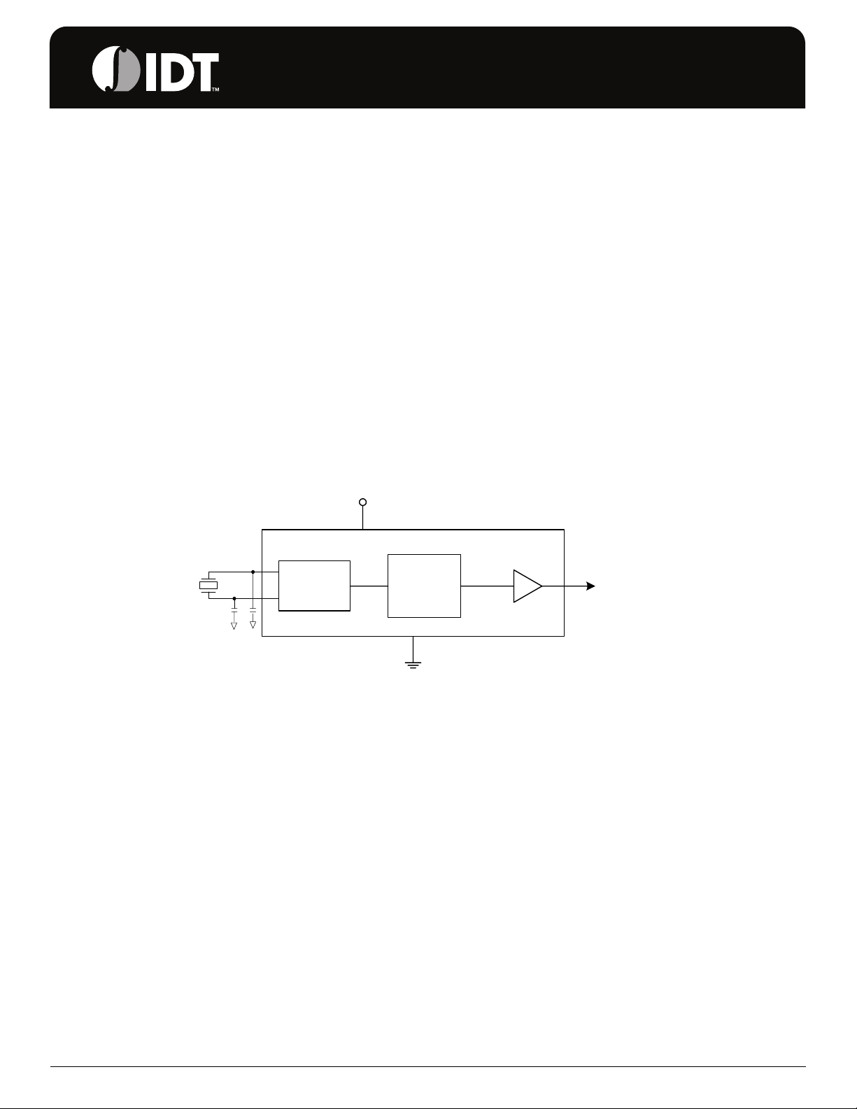
Block Diagram
VDD
X1
Crystal
Oscillator
X2
Features
• 14.31818 MHz crystal input
• The 48.00 MHz CLK output is USB2.0 reference clock
compliant
• Output duty cycle 45/55% (worst case)
• Advanced, low-power CMOS process
• Industrial temperature range (-40 to +85°C)
• Packaged in 5-pin TSOT
• 3.3 V supply voltage
• Pb (lead) free package available
• Short term C-C Jitter of 100 ps
PLL CLK
External capacitors are required
with a crystal input.
GND
IDT™ / ICS™
48 MHZ USB CLOCK SOURCE 1
ICS5OSK482 REV B 110805
Page 2
ICS5OSK482
48 MHZ USB CLOCK SOURCE SYNTHESIZERS
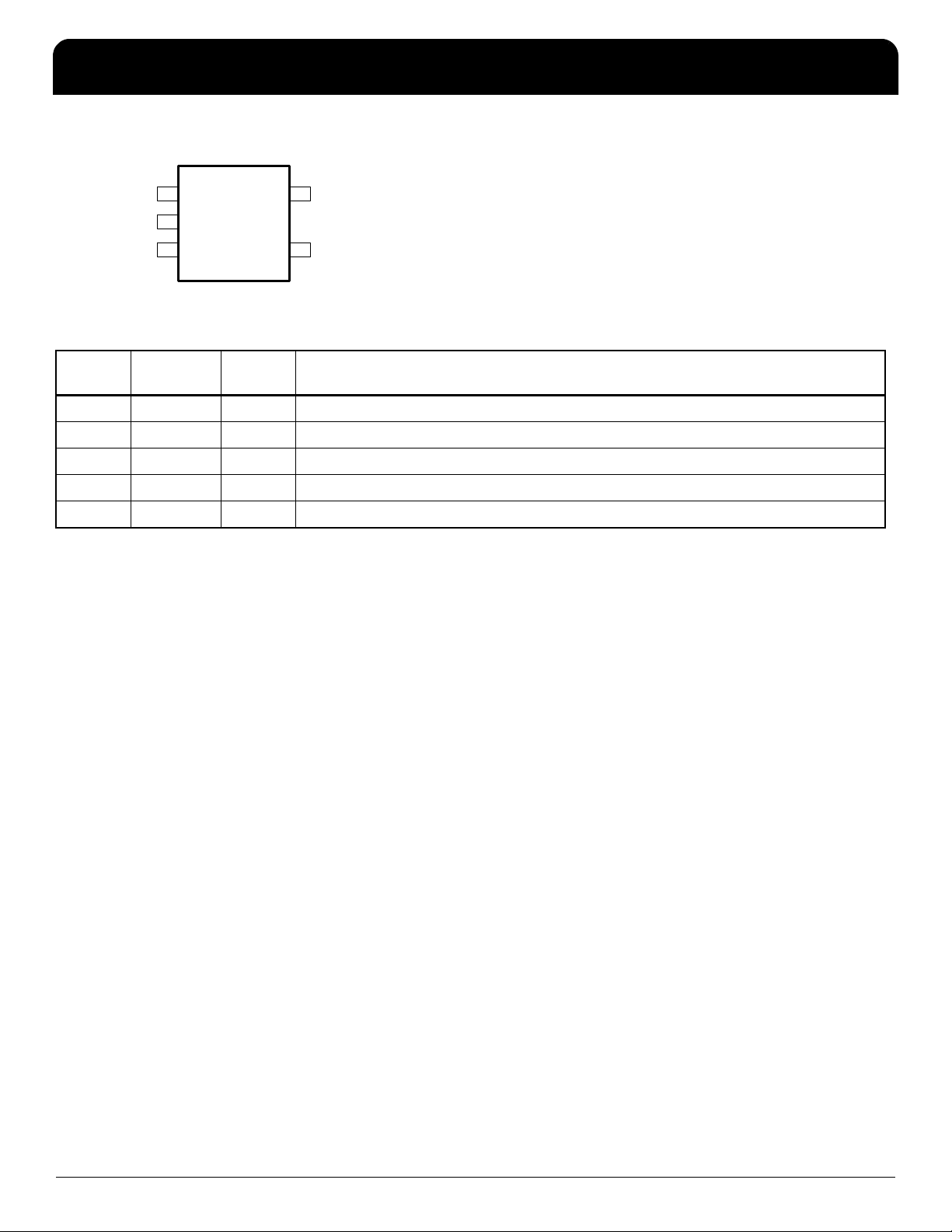
Pin Assignment
X1
GND
CLK
1
2
3
5
X2
VDD
4
Pin Descriptions
Pin
Number
1 X1 Input 14.31818 MHz crystal input. Connect to a parallel resonant fundamental crystal.
2 GND Power Connect to ground.
3 CLK Output PLL output clock. Internal pull-down resistor.
4 VDD Power Connect to 3.3 V.
5 X2 Output 14.31818 MHz crystal output.
Pin
Name
Pin
Typ e
Pin Description
External Components
External Crystal
The ICS5OSK482 requires a 14.31818 MHz crystal. In
order to minimize ppm errors, the PCB should include pads
for crystal capacitors from pins X1 to ground and X2 to
ground to optimize the initial accuracy. The capacitor value
can be determined by tuning the PCB so that the error on
the reference output is equal to the initial crystal error.
Crystal Load Capacitors
The device crystal connections should include pads for
small capacitors from pins X1 to ground and X2 to ground.
These capacitors are used to adjust the stray capacitance of
the board to match the nominally required crystal load
capacitance. Because load capacitance can only be
increased in this trimming process, it is important to keep
stray capacitance to a minimum by using very short PCB
traces (and no vias) between the crystal and device. Crystal
capacitors must be connected from each of the pins X1 and
X2 to ground.
The value (in pF) of these crystal caps should equal (C
pF) * 2. In the equation, C
= crystal load capacitance in pF.
L
Example: For a crystal with a 8 pF load capacitance, each
crystal capacitor would be 4 pF [(8-6) x 2 = 4].
IDT™ / ICS™
48 MHZ USB CLOCK SOURCE 2
L
-6
ICS5OSK482 REV B 110805
Page 3
ICS5OSK482
48 MHZ USB CLOCK SOURCE SYNTHESIZERS
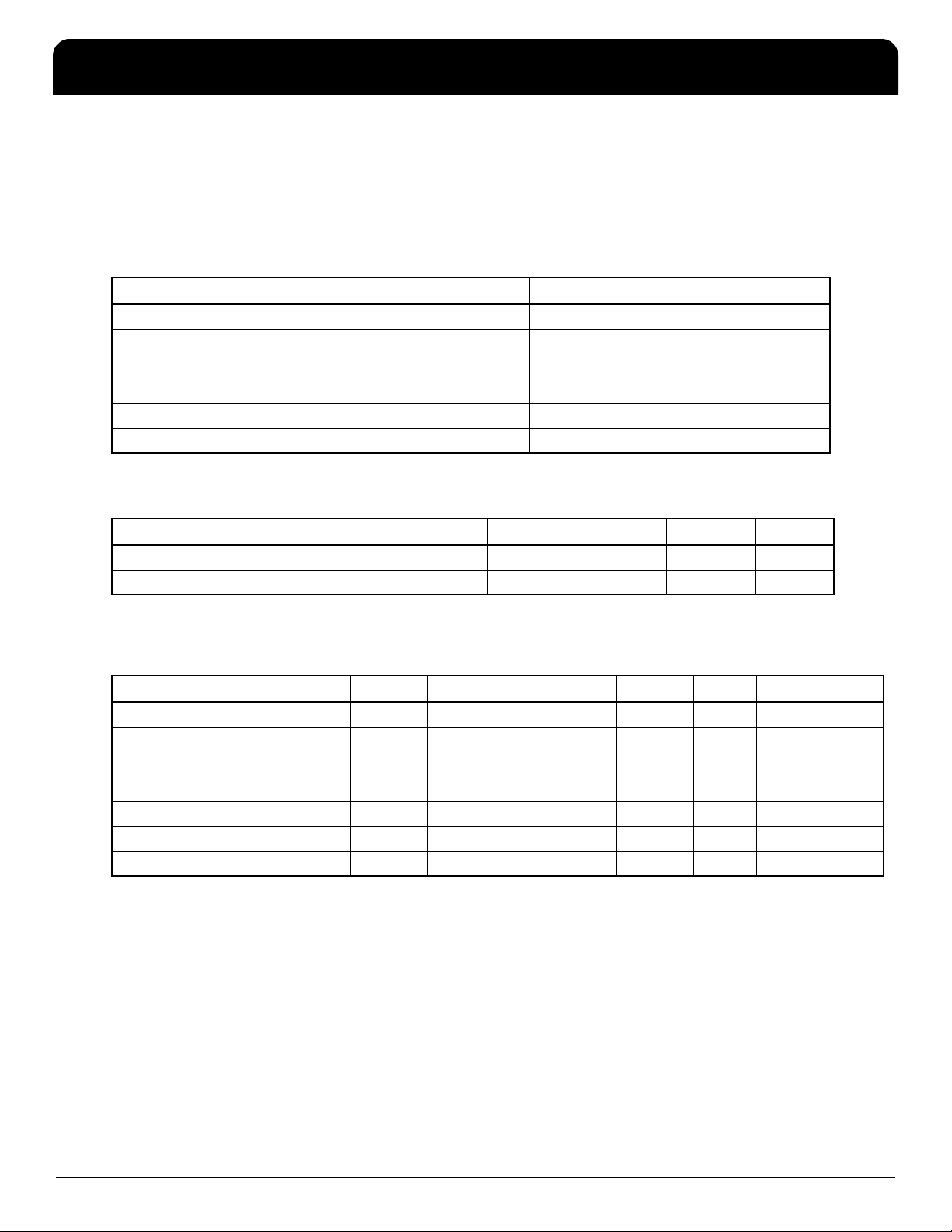
Absolute Maximum Ratings
Stresses above the ratings listed below can cause permanent damage to the ICS5OSK482. These ratings, which
are standard values for ICS commercially rated parts, are stress ratings only. Functional operation of the device at
these or any other conditions above those indicated in the operational sections of the specifications is not implied.
Exposure to absolute maximum rating conditions for extended periods can affect product reliability. Electrical
parameters are guaranteed only over the recommended operating temperature range.
Item Rating
Max Supply Voltage, VDD 7 V
Logic Inputs -0.5 V to VDD+0.5 V
Ambient Operating Temperature -40 to +85°C
Storage Temperature -65 to +150°C
Junction Temperature 125°C
Soldering Temperature 260°C
Recommended Operation Conditions
Parameter Min. Typ. Max. Units
Ambient Operating Temperature -40 +85 °C
Power Supply Voltage (measured in respect to GND) +3.135 +3.3 +3.465 V
DC Electrical Characteristics
VDD=3.3 V ±5%, Ambient temperature -40 to +85°C, CL = 15 pF, unless stated otherwise
Parameter Symbol Conditions Min. Typ. Max. Units
Operating Voltage VDD 3.135 3.465 V
Output High Voltage V
Output Low Voltage V
IDD Operating Supply Current IDD No Load TBD mA
Short Circuit Current I
Input Capacitance C
Nominal Output Impedance 20 Ω
OH
OL
OS
I
= -12 mA 2.4 V
OH
I
= 12 mA 0.4 V
OL
CLK output ±70 mA
IN
4pF
IDT™ / ICS™
48 MHZ USB CLOCK SOURCE 3
ICS5OSK482 REV B 110805
Page 4

ICS5OSK482
48 MHZ USB CLOCK SOURCE SYNTHESIZERS
AC Electrical Characteristics
VDD = 3.3 V ±5%, Ambient Temperature -40 to +85°C, CL = 15 pF, unless stated otherwise
Parameter Symbol Conditions Min. Typ. Max. Units
Input Frequency, crystal input f
Output Frequency f
Output Clock Rise Time t
Output Clock Fall Time t
Output Clock Duty Cycle t
Absolute Clock Period Jitter t
Note 1: Measured with a 15 pF load.
IN
OUT
OR
OF
DC
JA
0.8 to 2.0 V, Note 1 1 ns
2.0 to 0.8 V, Note 1 1 ns
1.5 V 45 50 60 %
Deviation from mean, Note 1 100 ps
14.31818 MHz
48 MHz
IDT™ / ICS™
48 MHZ USB CLOCK SOURCE 4
ICS5OSK482 REV B 110805
Page 5

ICS5OSK482
48 MHZ USB CLOCK SOURCE SYNTHESIZERS
Package Outline and Package Dimensions (5-pin TSOT)
Package dimensions are kept current with JEDEC Publication No. 95
Millimeters
Symbol Min Max
A — 1.00
A1 0.01 0.10
A2 0.84 0.90
b0.300.45
c0.120.20
D 2.90 BASIC
E 2.80 BASIC
E1 1.60 BASIC
e 0.95 BASIC
e1 1.90 BASIC
L0.300.50
L1 0.60 REF
L2 0.25 BASIC
θ
aaa — 0.10
0° 8°
Ordering Information
Part / Order Number Marking Shipping Packaging Package Temperature
ICS5OSK482TILF 2TIL Tubes 5-pin TSOT -40 to +85° C
ICS5OSK482TILFT 2TIL Tape and Reel 5-pin TSOT -40 to +85° C
Parts that are ordered with a “LF” suffix to the part number are the Pb-Free configuration and are RoHS compliant.
While the information presented herein has been checked for both accuracy and reliability, Integrated Circuit Systems (ICS) assumes no
responsibility for either its use or for the infringement of any patents or other rights of third parties, which would result from its use. No
other circuits, patents, or licenses are implied. This product is intended for use in normal commercial applications. Any other applications
such as those requiring extended temperature range, high reliability, or other extraordinary environmental requirements are not
recommended without additional processing by ICS. ICS reserves the right to change any circuitry or specifications without notice. ICS
does not authorize or warrant any ICS product for use in life support devices or critical medical instruments.
IDT™ / ICS™
48 MHZ USB CLOCK SOURCE 5
ICS5OSK482 REV B 110805
Page 6

ICS5OSK482
48 MHZ USB CLOCK SOURCE SYNTHESIZERS
Innovate with IDT and accelerate your future networks. Contact:
www.IDT.com
For Sales
800-345-7015
408-284-8200
Fax: 408-284-2775
Corporate Headquarters
Integrated Device Technology, Inc.
6024 Silver Creek Valley Road
San Jose, CA 95138
United States
800 345 7015
+408 284 8200 (outside U.S.)
© 2006 Integrated Device Technology, Inc. All rights reserved. Product specifications subject to change without notice. IDT an d the IDT logo are trademarks of Integrated Device
Technology, Inc. Accelerated Thinking is a service mark of Integrated D evice Technology, Inc. All other brands, product names and mar ks are or may be trademarks or registered
trademarks used to identify products or services of their respective owners.
Printed in USA
For Tech Support
<product line email>
<product line phone>
Asia Pacific and Japan
Integrated Device Technology
Singapore (1997) Pte. Ltd.
Reg. No. 199707558G
435 Orchard Road
#20-03 Wisma Atria
Singapore 238877
+65 6 887 5505
Europe
IDT Europe, Limited
321 Kingston Road
Leatherhead, Surrey
KT22 7TU
England
+44 1372 363 339
Page 7

 Loading...