

Page 1

EVK-UFT285-6-7 Evaluation Board User Guide
USER GUIDE
Introduction
The EVK-UFT285-6-7 is designed to help the customer evaluate the 8T49N285, 8T49N286, and 8T49N287 devices, members
of IDT's 3rd generation Universal Frequency Translator family. When the board is connected to a PC running IDT Timing
Commander™ software through USB, the device can be configured and programmed to generate frequencies with best-in-class
performances.
Contents
The EVK-UFT285-6-7 evaluation board ships with the following:
• 1 – EVK-UFT285-6-7 Evaluation Board
• 1 – USB Cable
Requirements
1. PC Requirements:
• IDT Timing Commander software installed.
• USB 2.0 interface. The evaluation board USB module is not compatible with USB 3.0. If using a computer with high speed
USB ports, please check if there's a standard USB 2.0 port available for use. The hardware drivers are automatically
installed during the Timing Commander installation.
• Windows XP SP3 or later.
• Processor: Minimum 1GHz.
• Memory: Minimum 512MB, recommended 1GB.
• Available Disk Space: Min 600MB (1.5GB 64bit), recommended 1GB (2GB 64bit)
• Network access during installation if the .NET framework is not currently installed on the system.
2. Power Supply with 3.3V and 1000mA rating
3. Three banana plug cables to connect the power supply to the board.
Quick Start: Powering Up the Board
(1) Set 3.3V supply current limit to 500mA.
(2) Remove all output terminations.
(3) Set Dip Switch selectors to the middle position.
(4) Connect a cable from a PC to the USB port.
(5) Connect VEE to the black GND jack.
(6) Connect 3.3V to VCC_J and VDDO_J.
(7) Power on the Power Supply.
(8) Press the Reset Button.
Once correct operation is verified, set the power supply limit for the number of outputs to be active.
The USB port must be powered by the PC in order to have the correct I
The board ships with a 38.88MHz crystal and will have a default frequency of 155.52MHz on Q0. If all outputs are unterminated,
current should measure ~256mA with 3.3V on VCC_J and VDDO_J. If all outputs are terminated, current should measure
~262mA.
When evaluating performance with the default hardware configuration, it is recommended that all active outputs be terminated
50ohms to VEE by either terminator plugs or an instrument.
2
C bus voltage levels.
REVISION B 04/01/15 1 ©2015 Integrated Device Technology, Inc.
Page 2
EVK-UFT285-6-7 EVALUATION BOARD USER GUIDE
8T49N286I_EVB
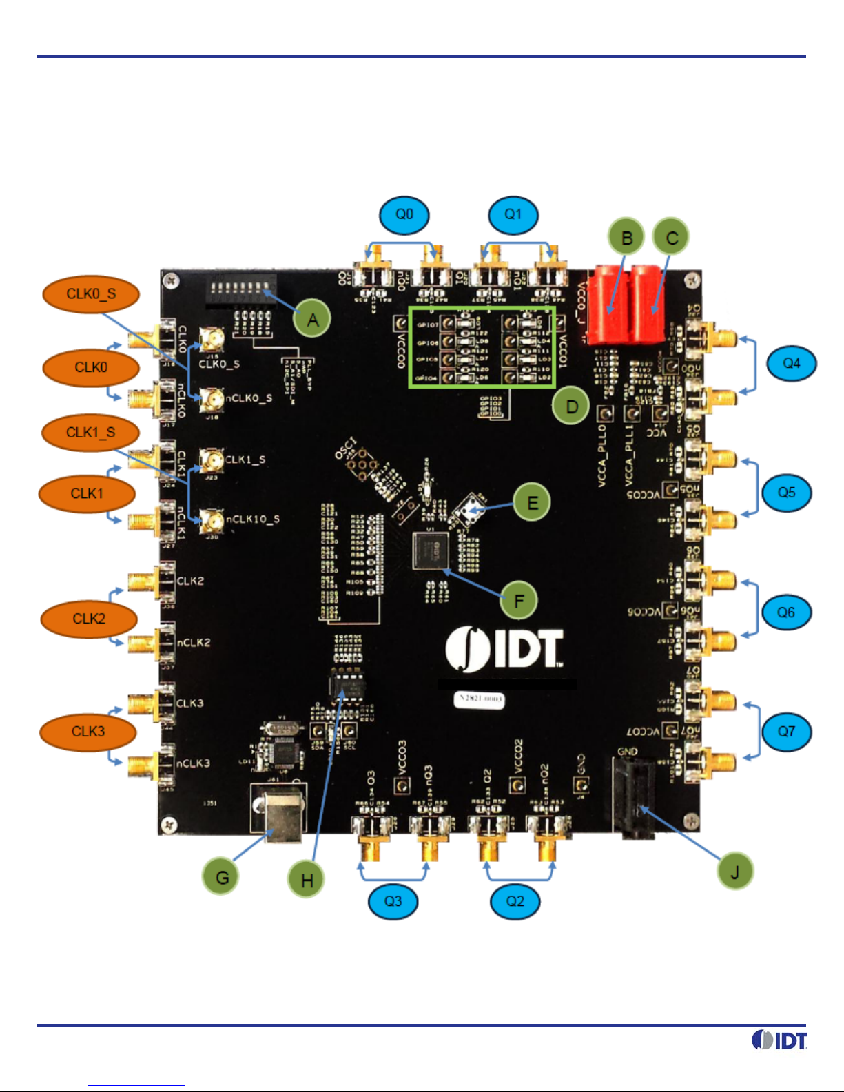
Board Overview
Use the following diagram to identify: power supply jacks, USB connector, input and output SMA connectors, reset button,
EEPROM, etc.
Figure 1. Evaluation Board Top View
REVISION B 04/01/15 2
Page 3

EVK-UFT285-6-7 EVALUATION BOARD USER GUIDE
Legend–Evaluation Board Top View
Inputs
CLK0_S Clock 0 sense lines.
CLK0 Clock 0 input lines. Can be configured for differential or single-ended input.
CLK1_S Clock 1 sense lines.
CLK1 Clock 1 input lines. Can be configured for differential or single-ended input.
CLK2 Clock 2 input lines. Can be configured for differential or single-ended input.
CLK3 Clock 3 input lines. Can be configured for differential or single-ended input.
Outputs
Q0 Output Q0. Can be a differential pair or two individual single-ended outputs.
Q1 Output Q1. Can be a differential pair or two individual single-ended outputs
Q2 Output Q2. Can be a differential pair or two individual single-ended outputs.
Q3 Output Q3. Can be a differential pair or two individual single-ended outputs.
Q4 Output Q4. Can be a differential pair or two individual single-ended outputs.
Q5 Output Q5. Can be a differential pair or two individual single-ended outputs.
Q6 Output Q6. Can be a differential pair or two individual single-ended outputs.
Q7 Output Q7. Can be a differential pair or two individual single-ended outputs.
Other
A Dip Switch for DC control signals (CLK_SEL, PLL_BYPASS, etc)
B VCCO_J
C VCC_J
D GPIOs
E RESET
F IDT8T49N286 – the device to be evaluated
G USB connector
H EEPROM – AT24CO4C
J Ground Jack
REVISION B 04/01/15 3
Page 4
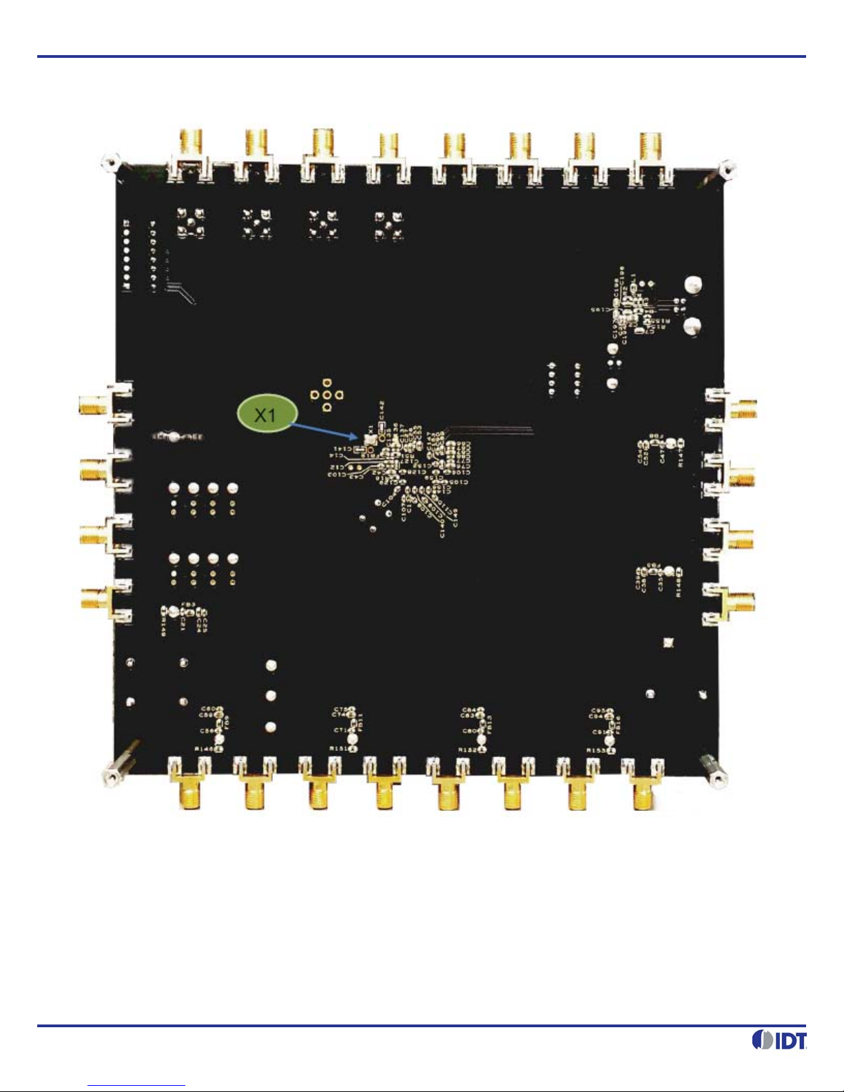
Figure 2. Evaluation Board Bottom View
EVK-UFT285-6-7 EVALUATION BOARD USER GUIDE
Legend–Evaluation Board Bottom View
X1 3.2 x 2.5 mm SMD Fox-603-38.88-4 Crystal
REVISION B 04/01/15 4
Page 5
EVK-UFT285-6-7 EVALUATION BOARD USER GUIDE
Schematics
The following figures are schematics that are applicable to specific sections of this User Guide. The complete schematics are
available in a separate document.
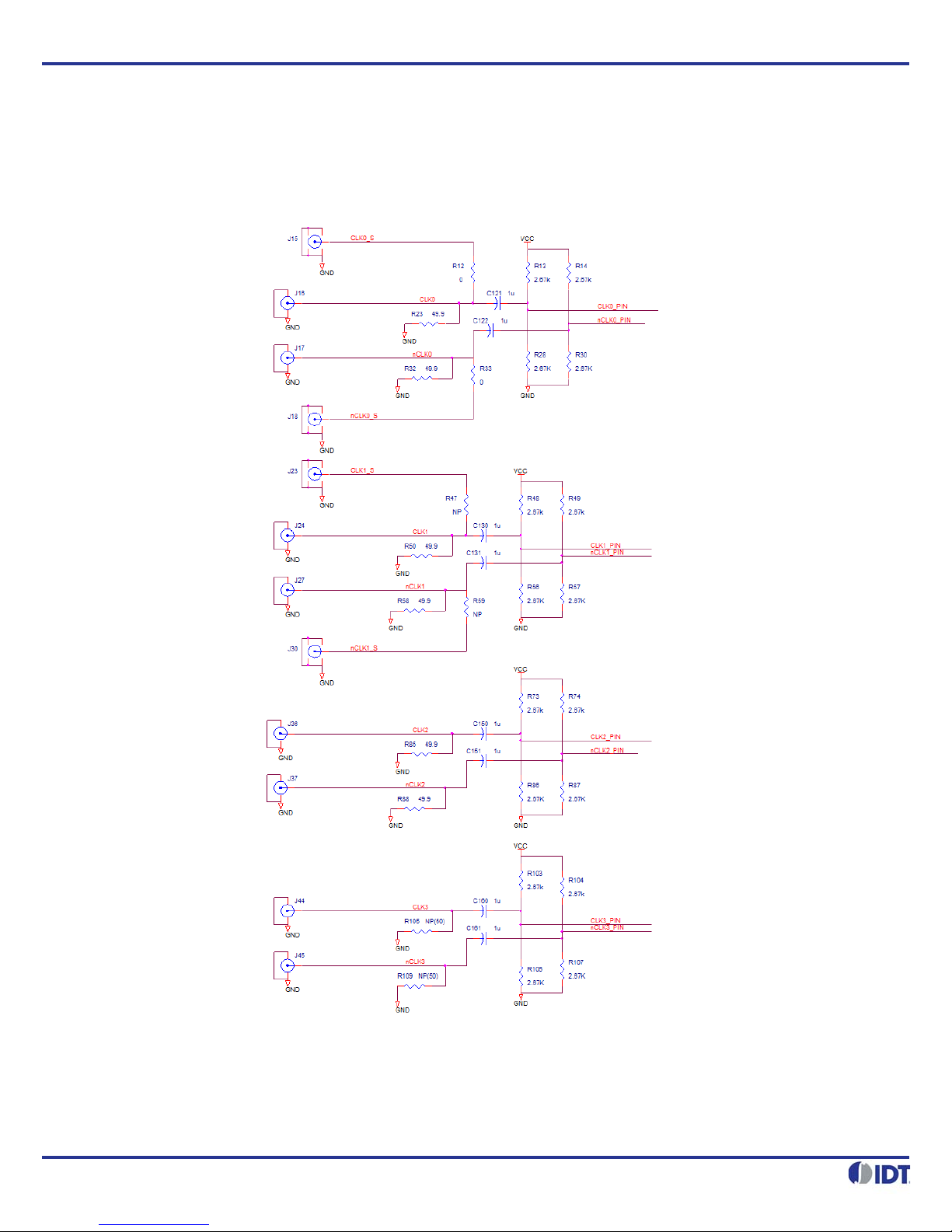
Figure 3. Inputs Schematic
REVISION B 04/01/15 5
Page 6
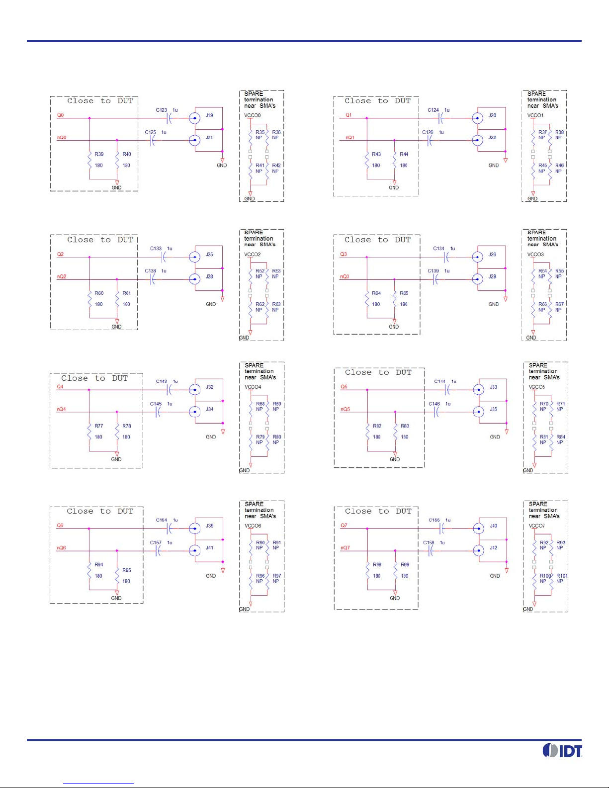
Figure 4. Output Termination Schematic
EVK-UFT285-6-7 EVALUATION BOARD USER GUIDE
REVISION B 04/01/15 6
Page 7
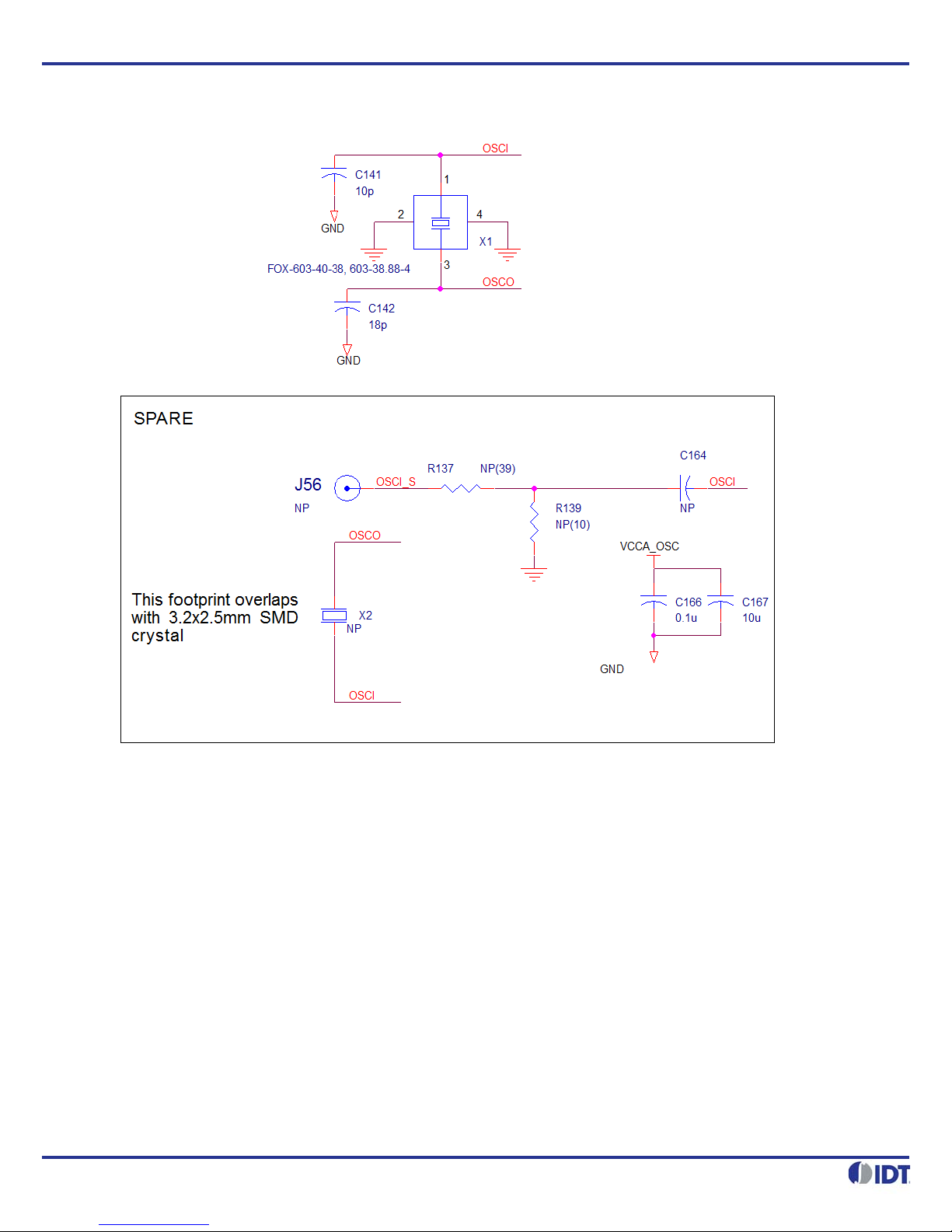
Figure 5. Crystal Interface Schematic
EVK-UFT285-6-7 EVALUATION BOARD USER GUIDE
REVISION B 04/01/15 7
Page 8

Figure 6. EEPROM/I2C Schematic
(If the device is programmed to boot from EEPROM, use
R156=0ohm, R131=1Kohm, and do not populate LD10)
(0 ohm in a system
design)
(1K ohm in a
system design)
EVK-UFT285-6-7 EVALUATION BOARD USER GUIDE
Figure 7. DC Control Schematic
REVISION B 04/01/15 8
Page 9

Figure 8. VCCO Power Filtering
EVK-UFT285-6-7 EVALUATION BOARD USER GUIDE
REVISION B 04/01/15 9
Page 10

Figure 9. VCC Filtering
Close to the DUT
FB18
BLM18B B221SN1D
C16
10uF
C89
10u
C55
0.1u
C119
10uF
C120
0.1u
C26
10u
C104
0.1u
C106
0.1u
J6
VCC_J
FB2
BLM18B B221SN1D
J5
GND
C42
10u
C62
10uF
GND
C108
0.1u
C12
10u
C103
0.1u
C14
0.1u
C43
0.1u
C110
0.1u
C76
10u
C88
0.1u
C63
0.1u
C13
0.1u
C65
10uF
J4
GND
C17
10uF
C105
0.1u
C15
0. 1 u
C90
0.1u
C61
0.1u
C67
0.1u
C87
10u
C27
0.1u
FB10
BLM18BB221SN1D
J14
VCC
C18
0.1u
C11
10uF
C107
0.1u
C77
0.1u
C53
10u
C66
10u
C109
0.1u
GND
GND
VCCO0
GND
VCCO1
GND
VCCO2
GND
VCCO3
GND GND
VCCO4 VCCO5 VCCO7VCCO6
GND
GND
GND
GND
VCC
GND
GND
GND
GND GND GND
VCC_J
VCCA_PLL0
Typ ~95mA
Typ ~95mA
VCCA_PLL1
VC CA_66
VC CA_71
VC CA_72
VC CA_70
VC CA_20
VC CA_19
VCCA_25
VC CA_21
VCCA_PLL1
C192
10uF
C193
0. 1u
VCCA_PLL0
EVK-UFT285-6-7 EVALUATION BOARD USER GUIDE
REVISION B 04/01/15 10
Page 11

EVK-UFT285-6-7 EVALUATION BOARD USER GUIDE
Board Power Supply
Core Voltages
The core voltage includes a digital voltage VDD and an analog voltage VDDA. Both core voltages are powered by the external
bench power supply connected to J6 (VCC_J). See Figure 9 for details
Output Voltages
VDDO_J (J1) supplies the global voltage for the outputs and can be biased by the external power supply at 1.8V (all outputs
LVCMOS), 2.5V, or 3.3V.
Mixed Voltage Operation
This board provides the option to operate the outputs with a mixed combination of output voltages. Refer to Figure 8 for a
complete view of the VCCO schematic. Each VCCOx has a 0 resistor that connects it to the global VCCO_J power rail. This
resistor can be removed and the voltage can be provided using the test point. For example, the schematic below can be
configured so that Q0 (VCCO0) operates at 2.5V and Q4 LVCMOS (VCCO4) operates at 1.8V as follows:
1) Connect 2.5V to J1 (VCCO_J).
2) Remove R146. This isolates VCCO4 from global VCCO_J.
3) Solder a wire onto test point VCCO4 and bias with a 1.8V supply.
Figure 10. Mixed Output Voltage Operation
REVISION B 04/01/15 11
Page 12

EVK-UFT285-6-7 EVALUATION BOARD USER GUIDE
Input Configuration
The inputs are configured with an ac-coupling termination scheme. This scheme allows flexibility for either differential or
single-ended inputs. The default configuration is as follows:
Table 1: Default Input Configuration
Input Default Termination Sense Lines
CLK0 50ohms to ground, ac-coupled into the device Use SMAs J15/J18 for observation of the input signal
CLK1 50ohms to ground, ac-coupled into the device Available but not connected. Populate R47 and R59 to observe
input signal on SMAs J23/J30
CLK2 50ohms to ground, ac-coupled into the device Not available
CLK3 50ohms to ground, ac-coupled into the device Not available
Differential Input
Connect the input signal to CLKx and nCLKx. For CLK0, the CLK0_S and nCLK0_s sense lines are available for observation of
the signal. They can be connected with 50ohm impedance cables to an oscilloscope with 50ohm termination, otherwise, they
should be terminated with 50ohm plugs in order prevent reflections.
Single-ended Input
Connect the input signal to CLKx and float nCLKx. For CLK0, connect CLK0_S with a 50ohm impedance cable to an oscilloscope
with 50ohm termination or terminate with a 50ohm plug.
Input Signals below 1MHz
For slow-frequency signals below 1MHz, we recommend that the coupling capacitors for the corresponding input be replaced
with zero-ohm resistors and that the signal input dc-offset be set so that it meets the device's Vcmr requirements. Refer to Figure
3 to locate the components listed below.
Table 2: Input Termination Schemes
AC-coupling capacitors:
CLK0 (C121, C122)
Signal Frequency
>1MHz 1µF Don't care
<1MHz Must meet datasheet Vcmr specs
CLK1 (C130,C131)
CLK2 (C150,C151)
CLK3 (C160,C161)
Input Signal DC Offset
REVISION B 04/01/15 12
Page 13

EVK-UFT285-6-7 EVALUATION BOARD USER GUIDE
Output Configuration
The outputs are ac-coupled, allowing for maximum flexibility for observation of the output whether configured for LVPECL, LVDS,
or LVCMOS levels. The default termination scheme can be used to measure either of the three output level-types but is not
optimal. The optimal termination circuits are tabulated below. Refer to Figure 4 to locate the components listed below.
Table 3: Termination Outputs for Q0
Signal Type 180 ohm pull-down:
R39, R40
LVPECL (Default) Installed 1µF Not installed
LVCMOS Not installed 33 ohm Not installed
LVDS Not installed 1µF Not installed
Series capacitors:
C123, C125
Resistor Network:
R35, R36, R41, R42
Table 4: Termination Outputs for Q1
Signal Type 180 ohm pull-down:
R43, R44
LVPECL (Default) Installed 1µF Not installed
LVCMOS Not installed 33 ohm Not installed
LVDS Not installed 1µF Not installed
Series capacitors:
C124, C126
Resistor Network:
R37, R38, R45, R46
Table 5: Termination Outputs for Q2
Signal Type 180 ohm pull-down:
R60, R61
LVPECL (Default) Installed 1µF Not installed
LVCMOS Not installed 33 ohm Not installed
Series capacitors:
C133, C138
Resistor Network:
R52, R53, R62, R63
LVDS Not installed 1µF Not installed
Table 6: Termination Outputs for Q3
Signal Type 180 ohm pull-down:
R64, R65
LVPECL (Default) Installed 1µF Not installed
LVCMOS Not installed 33 ohm Not installed
LVDS Not installed 1µF Not installed
Series capacitors:
C134, C139
Resistor Network:
R54, R55, R66, R67
Table 7: Termination Outputs for Q4
Signal Type 180 ohm pull-down:
R77, R78
LVPECL (Default) Installed 1µF Not installed
LVCMOS Not installed 33 ohm Not installed
LVDS Not installed 1µF Not installed
REVISION B 04/01/15 13
Series capacitors:
C143, C145
Resistor Network:
R68, R69, R79, R80
Page 14

Table 8: Termination Outputs for Q5
EVK-UFT285-6-7 EVALUATION BOARD USER GUIDE
Signal Type 180 ohm pull-down:
R82, R83
LVPECL (Default) Installed 1µF Not installed
LVCMOS Not installed 33 ohm Not installed
LVDS Not installed 1µF Not installed
Series capacitors:
C144, C146
Resistor Network:
R70, R71, R81, R84
Table 9: Termination Outputs for Q6
Signal Type 180 ohm pull-down:
R94, R95
LVPECL (Default) Installed 1µF Not installed
LVCMOS Not installed 33 ohm Not installed
LVDS Not installed 1µF Not installed
Series capacitors:
C154, C157
Resistor Network:
R90, R91, R96, R97
Table 10: Termination Outputs for Q7
Signal Type 180 ohm pull-down:
R98, R99
LVPECL (Default) Installed 1µF Not installed
LVCMOS Not installed 33 ohm Not installed
Series capacitors:
C155, C158
Resistor Network:
R92, R93, R100, R101
LVDS Not installed 1µF Not installed
As noted, the 4-resistor network is not installed in Tables 3~10 because an oscilloscope with internal 50 termination is utilized
for signal termination and measurement. If a DC-coupled, stand-alone LVPECL output is needed (without oscilloscope
connections), the 4-resistor network needs to be installed accordingly. The table below provides the configuration for Q0:
Table 11: Resistor Termination Outputs for LVPECL for Q0
Signal Type 180 ohm pull-down:
R39, R40
LVPECL (Default) Not installed 0 ohm R35=R36=125ohm
Series capacitors:
C123, C125
Resistor Network:
R35, R36, R41 R42
R41=R42=84ohm
Output signals below 1MHz
For slow-frequency output signals below 1MHz, we recommend that the 1µF ac-coupling capacitors be replaced with 0ohm
resistors and that the correct terminations be provided at the receiver.
REVISION B 04/01/15 14
Page 15

EVK-UFT285-6-7 EVALUATION BOARD USER GUIDE
EEPROM Boot
The evaluation board ships with an IDT8T49N286-997device, which will attempt to boot from the EEPROM at power-up. By
default, the EEPROM boot is not enabled on the board. If use of the EEPROM boot is required, there are three options to enable
this mode.
1) No Rework Option. This option will enable the EEPROM boot and does not require any soldering. This sequence must
be performed each time the EEPROM needs to be reloaded into the device.
a. Hold down the reset button.
b. Unplug and then plug in the USB cable.
c. Release the reset button.
2) Rework Option. This option will enable the EEPROM boot but requires soldering. It does not require continually
unplugging/plugging-in the USB cable for reloading of the EEPROM into the device.
a. Remove LD10 or replace R156 with a 1Kohm resistor. (See Figure 6).
b. Power up the board with USB cable connected.
c. Press and release the reset button.
3) Stand-Alone Use. Sometimes it's necessary to evaluate the device inside a temperature chamber, a system rack, or a
Faraday cage where a USB connection to the device is impractical. For such cases contact IDT for further support.
For details on how to program the EEPROM, please refer to document How to Program the 8T49N28x EEPROM.
DC Controls
The Dip Switch has three settings: 0V, Float, and VCC. This board ships with all switches in the Float (middle) position. Refer to
Figure 1, label "A" for the location of the Dip Switch.
REVISION B 04/01/15 15
Page 16

EVK-UFT285-6-7 EVALUATION BOARD USER GUIDE
Crystal Interface
By default, a 3.2x2.5mm SMD 38.88MHz crystal is installed on bottom side of the board. It provides the reference frequency for
the device. This board supports other options for the XTAL_IN reference. If using one of the other options, the crystal on X1 must
be removed.
1) Through-hole crystal. With this option, the device can be evaluated with different crystals without the need to solder each
time the crystal is replaced:
a. Remove the crystal from X1 on bottom-side of the board. (See Figure 2, "X1" for location of the component.)
b. Solder in crystal sockets into the holes labeled X2. (See Figure 11 below for location of the component.)
c. Place a crystal into the socket.
Figure 11. Crystal Interface PCB
2) Crystal Overdrive. With this option, the device can be evaluated with different sources, such as frequency generators,
XO's, or other devices. Refer to Figure 5 and Figure 10 for identification of the components mentioned below.
a. Remove the crystal from X1. (See Figure 2, "X1" for location of the component.)
b. Populate SMA J56.
c. Solder a 1µF capacitor onto C164. Note: the input must be ac-coupled
d. R139 may be populated with a 50ohm resistor for input sources requiring such termination.
e. R137 must be populated. It may be a 0ohm resistor for input sources or 33ohms for CMOS inputs.
REVISION B 04/01/15 16
Page 17

EVK-UFT285-6-7 EVALUATION BOARD USER GUIDE
Corporate Headquarters
6024 Silver Creek Valley Road
San Jose, CA 95138 USA
Sales
1-800-345-7015 or
408-284-8200
Tech Support
email: clocks@idt.com
480-763-2056
Fax: 408-284-2775
www.IDT.com
DISCLAIMER Integrated Device Technology, Inc. (IDT) and its subsidiaries reserve the right to modify the products and/or specifications described herein at any time and at IDT’s sole discretion. All information in this document,
including descriptions of product features and performance, is subject to change without notice. Performance specifications and the operating parameters of the described products are determined in the independent state and are not
guaranteed to perform the same way when installed in customer products. The information contained herein is provided without representation or warranty of any kind, whether express or implied, including, but not limited to, the
suitability of IDT’s products for any particular purpose, an implied warranty of merchantability, or non-infringement of the intellectual property rights of others. This document is presented only as a guide and does not convey any
license under intellectual property rights of IDT or any third parties.
IDT’s products are not intended for use in applications involving extreme environmental conditions or in life support systems or similar devices where the failure or malfunction of an IDT product can be reasonably expected to significantly affect the health or safety of users. Anyone using an IDT product in such a manner does so at their own risk, absent an express, written agreement by IDT.
Integrated Device Technology, IDT and the IDT logo are registered trademarks of IDT. Product specification subject to change without notice. Other trademarks and service marks used herein, including protected names, logos and
designs, are the property of IDT or their respective third party owners.
Copyright 2015. All rights reserved.
Page 18

Mouser Electronics
Authorized Distributor
Click to View Pricing, Inventory, Delivery & Lifecycle Information:
IDT (Integrated Device Technology):
EVK-UFT285-6-7
 Loading...