

Page 1

®
IDT™ 89EBPES4T4
Evaluation Board Manual
(Eval Board: 18-637-001)
August 2007
6024 Silver Creek Valley Road, San Jose, California 95138
Telephone: (800) 345-7015 • (408) 284-8200 • FAX: (408) 284- 2775
©2007 Integrated Device Technology, Inc.
Printed in U.S.A.
Page 2

Integrated Device Technology, Inc. reserves t h e right to make changes to its produc ts or specifications at any time, without notice, in order to improve design or perfor mance
and to supply the best possible product. IDT does not assume any responsibility for use of any circui try described other than the circuitry embodied in an IDT product. The
Company makes no representations that circuitry described herein is free from patent infringement or other rights of third parties which may result from its use. No license is
granted by implication or otherwise under any patent, patent rights or other rights, of Integrated Device Technology, Inc.
DISCLAIMER
Boards that fail to function should be returned to IDT for replacement. Credit will not be given for the failed boards nor will a
Failure Analy sis be performed.
Integrated Device Technology's products are not authorized for use as critical components in life support devices or systems unless a specific written agr eement pertaining to
such intended use is executed between the manufacturer and an officer of IDT.
1. Life support devices or systems are devices or systems which (a) are intended for su rgical implant into the body or (b) support or sustain life and whose failure to perform,
when properly us ed in accordance with instructions for use provided in the labeling, can be reasonably expected to res ult in a significant injury to the user.
2. A critical co mpo nent is an y com pon en t s of a lif e sup po rt dev ice or sy s te m who se f ai lu re t o perform can be re aso na bl y exp ect ed to cause the failure of the life support device
or system, or to affect its safety or effectiveness.
IDT, the IDT lo go, and Integrated Device Technology are trademarks or registered trademarks of I ntegrated Device Technology, Inc.
LIFE SUPPORT POLICY
Page 3

Table of Contents
®
Notes
Description of the EB4T4 Eval Board
Introduction.....................................................................................................................................1-1
Board Features...............................................................................................................................1-2
Hardware................................................................................................................................1-2
Software..................................................................................................................................1-2
Other.......................................................................................................................................1-2
Revision History..............................................................................................................................1-2
Installation of the EB4T4 Eval Board
EB4T4 Installation...........................................................................................................................2-1
Hardware Description.....................................................................................................................2-1
Host System...........................................................................................................................2-1
Reference Clocks............................................................................................................................2-1
Power Sources................................................................................................................................2-3
Vaux Support..........................................................................................................................2-3
PCI Express Serial Data Transmit Termination Voltage Converter........................................2-5
PCI Express Digital Power Voltage Converter........................................................................2-5
PCI Express Analog Power Voltage Converter......................................................................2-5
Core Logic Voltage Converter................................................................................................2-5
3.3V I/O Power Module...........................................................................................................2-5
Power-up Sequence...............................................................................................................2-5
Required Jumpers..................................................................................................................2-5
Reset...............................................................................................................................................2-5
Fundamental Reset................................................................................................................2-5
Downstream Reset.................................................................................................................2-6
Boot Configuration Vector...............................................................................................................2-6
SMBus Interfaces............................................................................................................................2-7
SMBus Master Interface.........................................................................................................2-7
Attention Buttons.............................................................................................................................2-7
Miscellaneous Jumpers, Headers...................................................................................................2-8
LEDs...............................................................................................................................................2-9
PCI Express Connectors...............................................................................................................2-10
EB4T4 Board Figure.....................................................................................................................2-12
Software for the EB4T4 Eval Board
Introduction.....................................................................................................................................3-1
Device Management Software........................................................................................................3-1
Schematics
Schematics.....................................................................................................................................4-1
EB4T4 Eval Board Manual i August 20, 2007
Page 4

IDT Table of Contents
Notes
EB4T4 Eval Board Manual ii August 20, 2007
Page 5

List of Tables
®
Notes
Table 2.1 Clock Source Selection .......................................................................................................2-1
Table 2.2 Spread Spectrum Clock Selection ......................................................................................2-2
Table 2.3 SMA Connectors - Onboard Reference Clock ....................................................................2-2
Table 2.4 Downstream Reset Selection .............................................................................................2-6
Table 2.5 Boot Configuration Vector Signals ......................................................................................2-6
Table 2.6 Boot Configuration Vector Switches S3 and S5 (ON=0, OFF=1) .......................................2-7
Table 2.7 JTAG Connector Pin Out ....................................................................................................2-7
Table 2.8 Attention Buttons ................................................................................................................2-8
Table 2.9 Miscellaneous Jumpers, Headers .......................................................................................2-8
Table 2.10 LED Indicators ....................................................................................................................2-9
Table 2.11 PCI Express x4 Connector Pinout ....................................................................................2-10
Table 2.12 PCI Express x1 Connector Pinout ....................................................................................2-11
EB4T4 Eval Board Manual iii August 20, 2007
Page 6

IDT List of Tables
Notes
EB4T4 Eval Board Manual iv August 20, 2007
Page 7

List of Figures
®
Notes
Figure 1.1 Function Block Diagram of the EB4T4 Eval Board ............................................................1-1
Figure 2.1 Clock Distribution Block Diagram .......................................................................................2-2
Figure 2.2 Power Distribution Block Diagram ......................................................................................2-3
Figure 2.3 APWRDIS# Timing ............................................................................................................2-4
Figure 2.4 APWRDIS# Timing Circuit .................................................................................................2-4
EB4T4 Eval Board Manual v August 20, 2007
Page 8

IDT List of Figures
Notes
EB4T4 Eval Board Manual vi August 20, 2007
Page 9
Chapter 1
Description of the EB4T4
Eval Board
®
Notes
Introduction
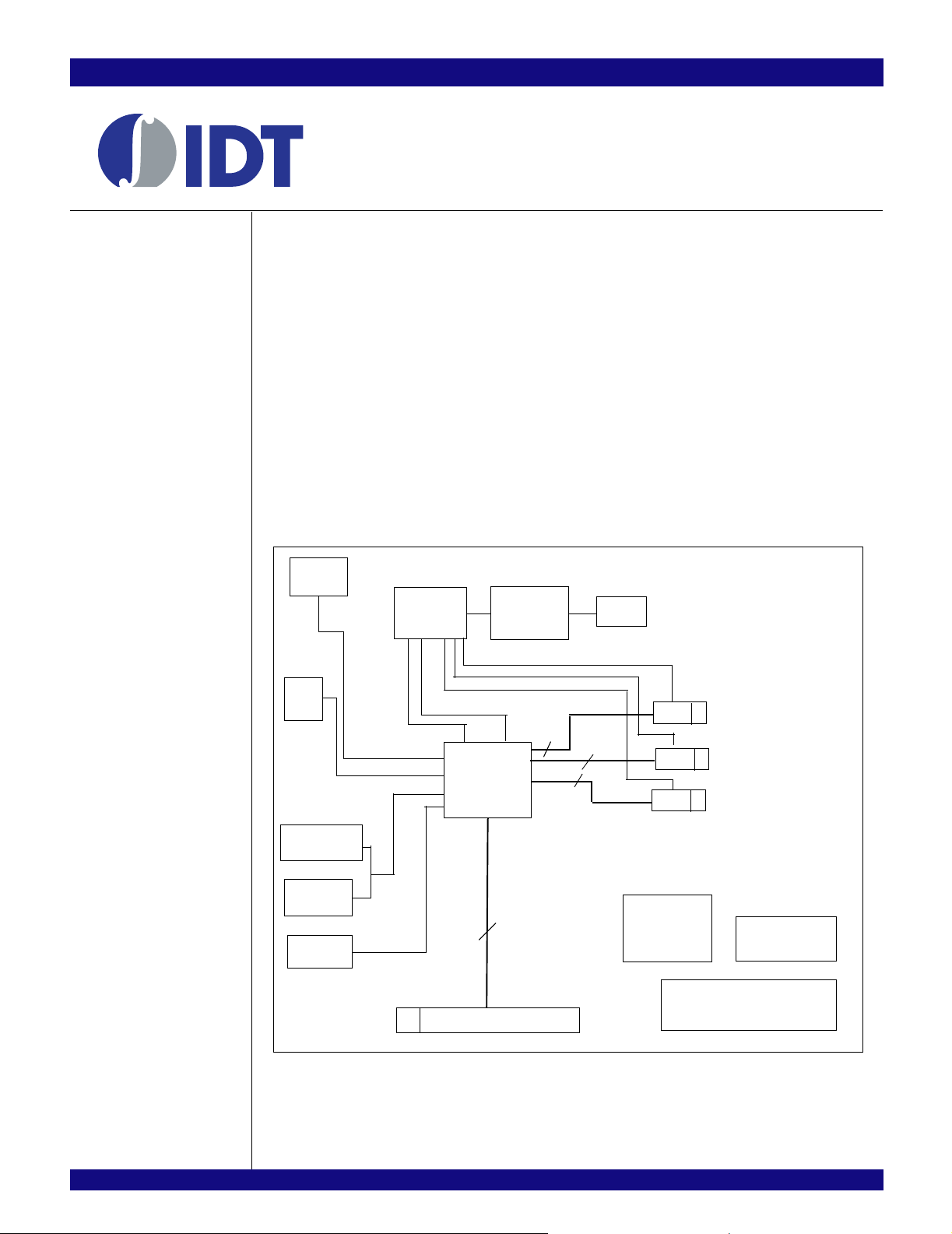
The 89HPES4T4 switch (also referred to as PES4T4 in this manual) is a member of IDT’s PCI Express®
standard (PCIe®) based line of products. It is an 4-lane, 4-port switch. One upstream port is provided for
connecting to the root complex (RC), and up to three downstream ports are available for connecting to PCIe
endpoints or to another switch. More information on this device can be found in the 89HPES4T4 User
Manual.
The 89EBPES4T4 Evaluation Board (also referred to as EB4T4 in this manual) provides an evaluation
platform for the PES4T4 switch. It is also a cost effective way to add a PCIe downstream port (x1) to an
existing system with a limited number of PCIe downstream ports. The EB4T4 eval board is designed to
function as an add-on card to be plugged into a x1 PCIe slot available on a motherboard hosting an appropriate root complex, microprocessor(s), and three downstream ports. The EB4T4 is a vehicle to test and
evaluate the functionality of the PES4T4 chip. Customers can use this board to get a headstart on software
development prior to the arrival of their own hardware. The EB4T4 is also used by IDT to reproduce
system-level hardware or software issues reported by customers. Figure 1.1 illustrates the functional block
diagram representing the main parts of the EB4T4 board.
JTAG
Header
Clock
Fanout
SSC Clock
Buffer
25 MHz
Main
Reset
I/O Expander
PCA9555
EEPROM
24LC512
SMBUS
HEADER
x1
PCI Express
Switch
PES4T4
SMBus
PCIe x1 Upstream Edge
Figure 1.1 Function Block Diagram of the EB4T4 Eval Board
x1
x1
x1
x1
Power
Module
PTH08T240
PCIe x1 Downstream Slot
PCIe x1 Downstream Slot
PCIe x1 Downstream Slot
External Power
Connector
Voltages on board
+12V, +3.3V, +1.5V, +1.0V
EB4T4 Eval Board Manual 1 - 1 August 20, 2007
Page 10

IDT Description of the EB4T4 Eval Board
Notes
Board Features
Hardware
PES4T4 PCIe 4 port switch
– Four ports (x1), 4 PCIe lanes
– PCIe Base Specification Revision 1.1 compliant
– Integrates four 2.5 Gbps embedded SerDes
– Up to 256 byte maximum Payload Size
– Automatic polarity inversion supported on all lanes
– Load configuration from an optional serial EEPROM via SMBUS
Upstream, Downstream Port
– One edge connector on the upstream port, to be plugged into a x1 slot on a host motherboard
– Three slot connectors on the downstream ports, for PCIe endpoint add-on cards to be plugged in.
Numerous user selectable configurations set using onboard jumpers and DIP-switches
– Source of clock - host clock or onboard clock generator
– One clock rate (100 MHz) and spread spectrum setting
– Boot mode selection
Vaux Support
SMBUS Master Interface connected to the Serial EEPROMs through I/O expander
“Attention” button for each downstream port to initiate a hot swap event on each port
Four pin connector for optional external power supply
Push button for Warm Reset
Several LEDs to display status, reset, power, “Attention”, etc.
One 10-pin JTAG connector (pitch 2.54 mm x 2.54 mm)
Software
There is no software or firmware executed on the board. However, useful software is provided along
with the Evaluation Board to facilitate configuration and evaluation of the PES4T4 within host systems
running popular operating systems.
Installation programs
– Operating Systems Supported: Windows2000, WindowsXP, Linux
GUI based application for Windows and Linux
– Allows users to view and modify registers in the PES4T4
– Binary file generator for programming the serial EEPROMs attached to the SMBUS.
Other
A metal bracket is required to firmly hold in place the three endpoints plugged into the EB4T4
board.
An external power supply may be required under some conditions.
SMBUS cable may be required for certain evaluation exercises.
SMA connectors are provided on the EB4T4 board for specific test points.
Revision History
August 20, 2007: Initial publication of board manual.
EB4T4 Eval Board Manual 1 - 2 August 20, 2007
Page 11

Chapter 2
Installation of the EB4T4
Eval Board
®
Notes
EB4T4 Installation
This chapter discusses the steps required to configure and install the EB4T4 evaluation board. All available DIP switches and jumper configurations are explained in detail.
The primary installation steps are:
1. Configure jumper/switch options suitable for the evaluation or application requirements.
2. Connect PCI Express endpoint cards to the downstream port PCIe slots on the evaluation board.
3. Insert the evaluation board into the host system (motherboard with root complex chipset).
4. Apply power to the host system.
The EB4T4 board is shipped with all jumpers and switches configured to their default settings. In most
cases, the board does not require further modification or setup.
Hardware Description
The PES4T4 is an 4-lane, 4-port PCI Express® switch. It is a peripheral chip that performs PCI Express
based switching with a feature set optimized for high performance applications such as servers and
storage. It provides fan-out and switching functions between a PCI Express upstream port and three downstream ports or peer-to-peer switching between downstream ports.
The EB4T4 has three PCI Express downstream ports, accessible through three x4 open-ended connectors.
Basic requirements for the board to run are:
– Host system with a PCI Express root complex supporting x4 configuration through a PCI Express
– PCI Express Endpoint Cards capable of training x1 link.
x1 slot.
Host System
The evaluation board cannot be operated as a standalone unit. A host system implementing a PCI
Express root complex supporting x1 configuration through a PCI Express x1 slot is required to take full
advantage of the PES4T4’s capabilities.
Reference Clocks
The PES4T4 uses one differential reference clock (100 MHz). The EB4T4 derives this clock from a
common source which is user-selectable. The common source can be either the host system’s reference
clock or the onboard clock generator. Selection is made by resistors described in Table 2.1.
Clock Configuration R32, R53, R51, R62
Installed Clock Source
R32, R53 Onboard Reference Clock – Use onboard clock generator
R51, R62 Upstream Reference Clock – Host system provides clock (Default)
Table 2.1 Clock Source Selection
EB4T4 Eval Board Manual 2 - 1 August 20, 2007
Page 12
IDT Installation of the EB4T4 Eval Board
Notes
The source for the onboard clock is the ICS9FG104 clock generator device (U8) connected to a 25MHz
oscillator (Y1). When using the onboard clock generator, the EB4T4 allows the selection of spread spectrum settings via DIP switches as described in Table 2.2 . Spread Spectrum technology reduces peak EMI
emissions by modulating the frequency to spread the peak energy over a wider bandwidth.
Clock Spread Spectrum Switch - S3[2]
S3[2] Spread Spectrum
OFF Enable Spread Spectrum
ON Disable Spread Spectrum (Default)
Table 2.2 Spread Spectrum Clock Selection
If the Clock Spread Spectrum is used to modulate data rate, then both ports must use same modulated
clock source. Therefore, if your system uses SSC, the on-board clock generator must be disabled and the
upstream reference clock should be used instead.
The output of the onboard clock generator is accessible through two SMA connectors located on the
Evaluation Board. See Table 2.3. This can be used to connect a scope for probing or capturing purposes
and cannot be used to drive the clock from an external source.
Onboard Reference Clock Output (Differential) – J3, J1
J3 Positive Reference Clock
J1 Negative Reference Clock
Table 2.3 SMA Connectors - Onboard Reference Clock
Figure 2.1 illustrates the clock distribution block diagram for the EB4T4 evaluation board.
Resistor Switch
PEREFCLK0
Upstream PEREFCLK
25MHz
ICS9DB803D
ISC9FG104
Figure 2.1 Clock Distribution Block Diagram
PEREFCLK1
Port2
Port3
Port4
SMA - J1
SMA - J3
EB4T4 Eval Board Manual 2 - 2 August 20, 2007
Page 13
IDT Installation of the EB4T4 Eval Board
Notes
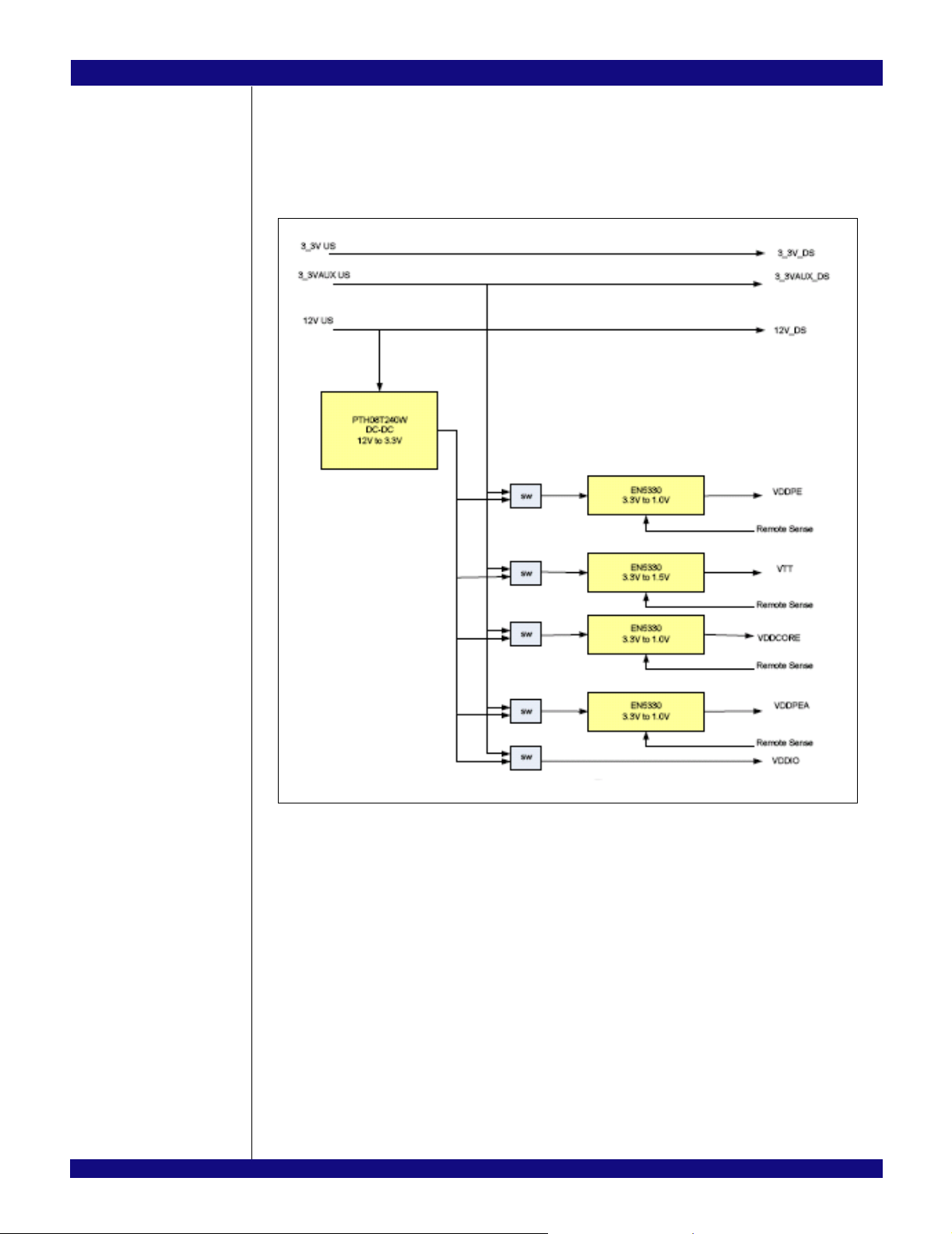
Power Sources
Power for the EB4T4 is generated from the 12.0V PCI Express upstream slot power or optionally from
3.3Vaux. A 12.0V to 3.3V DC-DC converter will be used to provide power to four DC-DC converters to
generate VDDcore, VDDpe, VDDpea, and VTT voltages. The 3.3V from the 12.0V converter is used to
power VDDio. When in power down mode the DC-DC converters is powered directly from 3.3Vaux through
a MOSFET switch.
Figure 2.2 Power Distribution Block Diagram
Vaux Support
Power supply support will be provided to EB4T4 from 12.0V upstream power to 3.3Vaux upstream
power when in sleep mode. The WAKE# signal direction, both an input and output will be supported by
jumper selection. The APWRDIS# signal for auxiliary power disable requires the following timing on powerup:
EB4T4 Eval Board Manual 2 - 3 a
Page 14

IDT Installation of the EB4T4 Eval Board
Notes
Figure 2.3 APWRDIS# Timing
On initial power up APWRDIS# must be held low initially for 8 clocks after PERST# i s removed. Then it
must be sampled high 256 clocks after PERSTN# is removed to enable L2 mode. Subsequent PERST# will
not affect the APWRDIS# state. This timing will be provided by the following circuit.
Figure 2.4 APWRDIS# Timing Circuit
EB4T4 Eval Board Manual 2 - 4 August 20, 2007
Page 15

IDT Installation of the EB4T4 Eval Board
Notes
PCI Express Serial Data Transmit Termination Voltage Converter
A DC-DC converter (U6) provides a 1.5V PCI Express serial data transmit termination voltage (shown
as VTTPE or VPETVTT) to the PES4T4.
PCI Express Digital Power Voltage Converter
A separate DC-DC converter (U16) provides a 1.0V PCI Express digital power voltage (VDDPE) to the
PES4T4.
PCI Express Analog Power Voltage Converter
A separate DC-DC converter (U7) provides a 1.0V PCI Express analog power voltage (shown as
VDDAPE or VDDPEA) to the PES4T4.
Core Logic Vo ltage Converter
A separate DC-DC converter (U1) provides the 1.0V core voltage (VDDCORE) to the PES4T4.
3.3V I/O Power Module
A 12V to 3.3V power module (U5) provides the 3.3V I/O voltage (VDDIO) to the PES4T4.
Power-up Sequence
The power-up sequence must be as following:
1. VDDIO - 3.3V
2. VDDCORE, VDDAPE, VDDPE - 1.0V
3. VTTPE - 1.5V
When powering up, each voltage level must ramp up and stabiliz e prior to applying the next voltage in
the sequence to ensure internal latch-up issues are avoided. There are no maximum time limitations
between sequential valid power level requirements. To insure that the sequencing requirements are met, a
0.047µF is used at the SOFTSTART cap on the VTTPE’s voltage converter (U6 pin 36) in the EB4T4.
Required Jumpers
To deliver power to the PES4T4 switch, the following jumpers must be shunted: W4, W10, W23, W24,
and W25. These jumpers were implemented so that the power consumption of the PES4T4 can be
measured.
Reset
The PES4T4 supports two types of reset mechanisms as described in the PCI Express specification:
– Fundamental Reset: This is a system-generated reset that propagates along the PCI Express
tree through a single side-band signal PERST# which is connected to the Root Complex, the
PES4T4, and the endpoints.
– Hot Reset: This is an In-band Reset, communicated downstream via a link from one device to
another. Hot Reset may be initiated by software. This is further discussed in the 8 9HPES8T4 User
Manual. The EB4T4 evaluation board provides seamless support for Hot Reset.
Fundamental R eset
There are two types of Fundamental Resets which may occur on the EB4T4 evaluation board:
– Cold Reset: During initial power-on, the onboard voltage monitor (TLC7733D) will assert the PCI
Express Reset (PERSTN) input pin of the PES4T4.
– Warm Reset: This is triggered by hardware while the device is powered on. Warm Reset can be
initiated by two methods:
• Pressing a push-button switch (S1) located on EB4T4 board
EB4T4 Eval Board Manual 2 - 5 a
Page 16

IDT Installation of the EB4T4 Eval Board
Notes
• The host system board IO Controller Hub asserting PERST# signal, which propagates through
the PCIe upstream edge connector of the EB4T4. Note that one can bypass the onboard voltage
monitor (TLC7733D) by moving the shunt from pin 1-2 to pin 2-3 (default) on W2.
Both events cause the onboard voltage monitor (TLC7733D) to assert the PCI Express Reset
(PERSTN) input of the PES4T4 while power is on.
Downstream Reset
The PES4T4 provides a a choice of either a software-controlled reset for each downstream port through
GPIO pins or a fundamental reset through PERST#. Selection is made by jumpers described in Table 2.4.
Port # Jumper Selection
4 W9 [1-2] Software controlled reset through GPIO1
[2-3] Fundamental reset PERST# (default)
3 W6 [1-2] Software controlled reset through GPIO9
[2-3] Fundamental reset PERST# (default)
2 W7 [1-2] Software controlled reset through GPIO0
[2-3] Fundamental reset PERST# (default)
Table 2.4 Downstream Reset Selection
Boot Configuration Vector
A boot configuration vector consisting of the signals listed in Table 2.5 is sampled by the PES4T4 during
a fundamental reset (while PERSTN is active). The boot configuration vector defines the essential parameters for switch operation and is set using DIP switches S3 and S5 as defined in Table 2.6.
Signal Description
CCLKDS Common Clock Downstream. When the CCLKDS pin is asserted, it indicates that a com-
mon clock is being used between the downstream device and the downstream port.
Default: 0x1
CCLKUS Common Clock Upstream. When the CCLKUS pin is asserted, it indicates that a common
clock is being used between the upstream device and the upstream port. Default: 0x1
RSTHALT Reset Halt. When this signal is asserted during a PCI Express fundamental reset, the
PES4T4 executes the reset procedure and remains in a reset state with the Master SMBus
active. This allows software to read and write registers internal to the device before normal
device operation begins. The device exits the reset state when the RSTHALT bit is cleared
in the P0_SWCTL register through the SMBus.
The value may be overridden by modifying the RSTHALT bit in the P0_SWCTL register.
Default: 0x0
SWMODE[2:0] Switch Mode. These configuration pins determine the PES4T4 switch operating mode.
Default: 0x1
0x0 - Normal switch mode
0x1 - Normal switch mode with Serial EEPROM-based initialization
0x2 through 0x8 - Reserved
APWRDIS# Auxiliary Power Disable. When this pin is active, it disables the device from using auxil-
iary power supply. Default: 0x0
Table 2.5 Boot Configuration Vector Signals
EB4T4 Eval Board Manual 2 - 6 August 20, 2007
Page 17

IDT Installation of the EB4T4 Eval Board
Notes
Table 2.6 Boot Configuration Vector Switches S3 and S5 (ON=0, OFF=1)
SMBus Interfaces
The System Management Bus (SMBus) is a two-wire interface through which various system component chips can communicate. It is based on the principles of operation of I
signals in the PCI Express connector is optional and may not be present on the host system. The SMBus
interface consist of an SMBus clock pin and SMBus data pin.
SMBus Master Interface
Connected to the master SMBus interface are four 16-bit I/O Expanders (PCA9555) and a serial
EEPROM (24LC512). Four I/O Expanders are used as the interface for the onboard hot-plug controllers
(MIC2591B). The Master SMBus interface provides connection to the external serial EEPROMs used for
initialization and the I/O expander used for hot-plug signals.
Signal Description Default
S3[4] CCLKDS OFF
S3[5] CCLKUS OFF
S5[6] RSTHALT ON
S5[1] SWMODE[0] ON
S5[2] SWMODE[1] ON
S5[3] SWMODE[2] ON
S5[5] APWRDIS# ON
2
C. Implementation of the SMBus
The bus address for the selected EEPROM device is 0b1010011
by default.
The PES4T4 provides a JTAG connector J4 for access to the PES4T4 JTAG interface. The connector is
a 2.54 x 2.54 mm pitch male 10-pin connector. Refer to Table 2.9 for the JTAG Connector J2 pin out.
JTA G Connector J2
Pin Signal Direction Pin Signal Direction
1 /TRST - Test reset Input 2 GND —
3 TDI - Test data Input 4 GND —
5 TDO - Test data Output 6 GND —
7 TMS - Test mode select Input 8 GND —
9 TCK - Test clock Input 10 GND —
Table 2.7 JTAG Connector Pin Out
Attention Buttons
The PES4T4 features four attention buttons, shown in Table 2.10. Each button corresponds to a particular port and is used to initiate hot-swapping events.
EB4T4 Eval Board Manual 2 - 7 a
Page 18

IDT Installation of the EB4T4 Eval Board
Notes
Miscellaneous Jumpers, Headers
Button Description
SW3 Port 4 Attention Button
SW2 Port 3 Attention Button
SW1 Port 2 Attention Button
Table 2.8 Attention Buttons
Miscellaneous Jumpers, Headers
Ref.
Designator
S2[1] Switch OFF Port2: Manually-operated Retention Latch
S2[2] Switch OFF Port3: Manually-operated Retention Latch
S2[3] Switch OFF Port4: Manually-operated Retention Latch
S6[3] Switch OFF Bypass hot-plug controller - Enables direct power (+12V and
S6[2] Switch OFF Bypass hot-plug controller - Enables direct power (+12V and
S6[1] Switch OFF Bypass hot-plug controller - Enables direct power (+12V and
W32 Header 2-3 Shunted 1-2: Port 2, +3.3V source base on hot-plug controller
W31 Header 2-3 Shunted 1-2: Port 2, +12V source base on hot-plug controller
W30 Header 2-3 Shunted 1-2: Port 2, +3.3Vaux source base on hot-plug controller
W35 Header 2-3 Shunted 1-2: Port 3, +3.3V source base on hot-plug controller
W34 Header 2-3 Shunted 1-2: Port 3, +12V source base on hot-plug controller
Type Default Description
+3.3V) to Ports 4 (Default)
+3.3V) to Ports 3 (Default)
+3.3V) to Ports 2 (Default)
2-3: Port 2, +3.3V source from upstream port power
2-3: Port 2, +12V source from upstream port power
2-3: Port 2, +3.3Vaux source from upstream port power
2-3: Port 3, +3.3V source from upstream port power
2-3: Port 3, +12V source from upstream port power
W33 Header 2-3 Shunted 1-2: Port 3, +3.3Vaux source base on hot-plug controller
2-3: Port 3, +3.3Vaux source from upstream port power
W38 Header 2-3 Shunted 1-2: Port4, +3.3V source base on hot-plug controller
2-3: Port 4, +3.3V source from upstream port power
W37 Header 2-3 Shunted 1-2: Port 4, +12V source base on hot-plug controller
2-3: Port 4, +12V source from upstream port power
W36 Header 2-3 Shunted 1-2: Port 4, +3.3Vaux source base on hot-plug controller
2-3: Port 4, +3.3Vaux source from upstream port power
W15 Header Open 1-2: Select WAKEN# as an input
2-3: Select WAKE# as in output
Table 2.9 Miscellaneous Jumpers, Headers (Part 1 of 2)
EB4T4 Eval Board Manual 2 - 8 August 20, 2007
Page 19

IDT Installation of the EB4T4 Eval Board
Notes
Miscellaneous Jumpers, Headers
Ref.
Designator
W17 Header Shunted Power Good Enable Force On jumper for ICS90DB803 clock
W18 Header Shunted Power Good Enable Force On jumper for ICS90DB803 clock
W19 Header Shunted Power Good Enable Force On jumper for ICS90DB803 clock
W5 Header Open Special usage when there is no +12V power supply from the
Type Default Description
output enable (OE4#)
output enable (OE3#)
output enable (OE2#)
upstream port. Require external power to connector J4.
Table 2.9 Miscellaneous Jumpers, Headers (Part 2 of 2)
LEDs
There are several LED indicators on the EB4T4 which convey status feedback. A description of each is
provided in Table 2.13.
Location Color Definition
DS87 Green Port 2: Power-is-good indicator
DS86 Green Port 3: Power-is-good indicator
DS85 Green Port 4: Power-is-good indicator
DS83 Amber Port2: Attention Input indicator
DS82 Amber Port3: Attention Input indicator
DS81 Amber Port4: Attention Input indicator
DS79 Green Port2: Presence Detect indicator
DS78 Green Port3: Presence Detect indicator
DS77 Green Port4: Presence Detect indicator
DS64 Amber Port2: Attention Output indicator
DS63 Amber Port3: Attention Output indicator
DS62 Amber Port4: Attention Output indicator
DS57 Green Port 2: Power indicator
DS56 Green Port 3: Power indicator
DS55 Green Port 4: Power indicator
DS91 Red Port 2: MRL indicator
DS90 Red Port 3: MRL indicator
DS89 Red Port 4: MRL indicator
DS95 Red Port 2: Power Fault indicator
DS94 Red Port 3: Power Fault indicator
DS93 Red Port 4: Power Fault indicator
Table 2.10 LED Indicators (Part 1 of 2)
EB4T4 Eval Board Manual 2 - 9 a
Page 20

IDT Installation of the EB4T4 Eval Board
Notes
Location Color Definition
DS99 Green Port 2: Link Up indicator
DS98 Green Port 3: Link Up indicator
DS97 Green Port 4: Link Up indicator
DS100 Green Port 0: Link Up indicator
DS105 Amber Port0: Link Activity indicator
DS104 Amber Port2: Link Activity indicator
DS103 Amber Port3: Link Activity indicator
DS102 Amber Port4: Link Activity indicator
Table 2.10 LED Indicators (Part 2 of 2)
PCI Express Connectors
Pin Side A Side B
1 +12V 12V power PRSNT1# Hot-Plug presence detect
2 +12V 12V power +12V 12V power
3 RSVD Reserved +12V 12V power
4 GND Ground GND Ground
5 SMCLK SMBus clock JTAG2 TCK (Test Clock) JTAG i/f clk i/p
6 SMDAT SMBus Data JTAG TDI (Test Data Input)
7 GND Ground JTAG TDO (Test Data Output)
8 +3.3V 3.3V power JTAG TMS (Test Mode Select)
9 JTAG1 TRST# (Test/Reset) resets
JTAG i/f
10 3.3Vaux 3.3V auxiliary power +3.3V 3.3V power
11 WAKE# Signal for Link reactivation PERST# Fundamental Reset
Mechanical Key
12 RSVD Reserved GND Ground
13 GND Ground REFCLK+ REFCLK Reference clock
14 PETp0 Transmitter differential REFCLK- (differential pair)
15 PETn0 pair, Lane 0 GND Ground
16 GND Ground PERp0 Receiver differential
17 PRSNT2# Hot-Plug presence detect PERn0 pair, Lane 0
18 GND Ground GND Ground
19 PETp1 Transmitter differential RSVD Reserved
+3.3V 3.3V power
20 PETn1 pair, Lane 1 GND Ground
21 GND Ground PERp1 Receiver differential
Table 2.11 PCI Express x4 Connector Pinout (Part 1 of 2)
EB4T4 Eval Board Manual 2 - 10 August 20, 2007
Page 21

IDT Installation of the EB4T4 Eval Board
Notes
Pin Side A Side B
22 GND Ground PERn1 pair, Lane 1
23 PETp2 Transmitter differential GND Ground
24 PETn2 pair, Lane 2 GND Ground
25 GND Ground PERp2 Receiver differential
26 GND Ground PERn2 pair, Lane 2
27 PETp3 Transmitter differential GND Ground
28 PETn3 pair, Lane 3 GND Ground
29 GND Ground PERp3 Receiver differential
30 RSVD Reserved PERn3 pair, Lane 3
31 PRSNT2# Hot-Plug presence detect GND Ground
32 GND Ground RSVD Reserved
Table 2.11 PCI Express x4 Connector Pinout (Part 2 of 2)
Pin Side A Side B
1 +12V 12V power PRSNT1# Hot-Plug presence detect
2 +12V 12V power +12V 12V power
3 RSVD Reserved +12V 12V power
4 GND Ground GND Ground
5 SMCLK SMBus clock JTAG2 TCK (Test Clock) JTAG i/f clk i/p
6 SMDAT SMBus Data JTAG TDI (Test Data Input)
7 GND Ground JTAG TDO (Test Data Output)
8 +3.3V 3.3V power JTAG TMS (Test Mode Select)
9 JTAG1 TRST# (Test/Reset)
resets JTAG i/f
10 3.3Vaux 3.3V auxiliary power +3.3V 3.3V power
11 WAKE# Signal for Link reactiva-
tion
Mechanical Key
12 RSVD Reserved GND Ground
13 GND Ground REFCLK+ REFCLK Referenc e clock
14 PETp0 Transmitter differential REFCLK- (differential pair)
15 PETn0 pair, Lane 0 GND Ground
16 GND Ground PERp0 Receiver differential
17 PRSNT2# Hot-Plug presence detect PERn0 pair, Lane 0
18 GND Ground GND Ground
+3.3V 3.3V power
PERST# Fundamental Reset
Table 2.12 PCI Express x1 Connector Pinout
EB4T4 Eval Board Manual 2 - 11 a
Page 22

IDT Installation of the EB4T4 Eval Board
Note: These x4 and x1 PCI Express connectors comply with the PCIe specification. The EB4T4 uses x1 connector on all downstream
ports. According to the PCI Express specification, the PRSNT1# pin should be wired to the farthest available PRSNT2# pin on the
connector. In the EB4T4, all PRSNT2# pins are tied together. This allows the board to be installed in a x1 or a x4 slot. The open-ended x4
slot allows the insertion of physical lane width greater than x4 to be installed without the need of slot reducer.
EB4T4 Board Figure
EB4T4 Eval Board Manual 2 - 12 August 20, 2007
Page 23

Chapter 3
Software for the EB4T4 Eval Board
®
Notes
Introduction
This chapter discusses some of the main features of the available software to give users a better under-
standing of what can be achieved with the EB4T4 evaluation board using the device management software.
Device management software and related user documentation are available on a CD which is included
in the Evaluation Board Kit. This information is also available on IDT’s FTP site. For more information,
contact IDT at ssdhelp@idt.com.
Device Management Software
The primary use of the Device Management Software package is to enable users of the evaluation
board to access all the registers in the PES4T4 device. This access can be achieved using the PCI Express
in-band configuration cycles through the upstream port on the PES4T4.
This software also enables users to save a snapshot of the current register set into a dump file which
can be used for debugging purposes. An export/import facility is also available to create and use “Configuration” files which can be used to initialize the switch device with specific values in specific registers.
A conversion utility is also provided to translate a configuration file into an EEPROM programmable data
structure. This enables the user to program an appropriate serial EEPROM with desirable register settings
for the PES4T4, and then to populate that EEPROM onto the Evaluation Board. It is also possible to
program the EEPROM directly on the Evaluation Board using a feature provided by the software package.
The front end of the Device Management Software is a user-friendly Graphical User Interface which
allows the user to quickly read or write the registers of interest. The GUI also permits the user to run the
software in “simulation” mode with no real hardware attached, allowing the creation of configuration files for
the PES4T4 in the absence of the actual device.
Much of the Device Management Software is written with device-independent and OS-independent
code. The software will be guaranteed to work on Linux (/sys interface) and MS Windows XP. It may function flawlessly on various flavors of MS Windows, but may not be validated on all. The fact that the software
is device-independent assures its scalability to future PCIe parts from IDT. Onc e users are familiar with the
GUI, they will be able to use the same GUI on all PCIe parts from IDT. This software is customized for each
device through an XML device description file which includes information on the number of ports, registers,
types of registers, information on bit-fields within each register, etc.
EB4T4 Eval Board Manual 3 - 1 August 20, 2007
Page 24

IDT Software for the EB4T4 Eval Board
Notes
EB4T4 Eval Board Manual 3 - 2 August 20, 2007
Page 25

Chapter 4
Schematics
®
Notes
Schematics
EB4T4 Eval Board Manual 4 - 1 August 20, 2007
Page 26

8
6
57
4
3
DCN
STGC-0117 1.0 INITIAL RELEASE 2007-06-18 J.CARRILLO
REV
2
DESCRIPTION
REVISIONS
DATE
1
CHANGE BY
D
SHEET
1
2
3
4
5
6
7
8
9
DESCRIPTION
TABLE OF CONTENTS
POWER REGULATORS PES4T4
POWER MOSFETS FOR 3.3VAUX
CLOCKS
RESET,SMBUS,JTAG,DIPSW
APWRDISN TIMING CIRCUIT
EPROM ATTN_SW WAKE
IO EXPANDERS
IO EXPANDER LEDS
D
CC
10
11
12
13
14
15
16
17
A
HOT SWAP CONTROL PORT 2/4
HOT SWAP CONTROL PORT 3
PES4T4 - CLOCK,SMBUS,GPIO
PES4T4 - PORT 0
PES4T4 - DOWNSTREAM PORTS
DOWNSTREAM PORT 2/3 CONNECTORS
DOWNSTREAM PORT 4 CONNECTORS
PES4T4 - POWER
TITLE
BB
A
89EBPES4T4 Evaluation Board
DRAWING NO.
SIZE
STGSCH-00117
B
CONFIDENTIAL PROPERTY OF INTEGRATED DEVICE TECHNOLOGY, INC.
6024 SILVER CREEK VALLEY RD. SAN JOSE, CA 95138
COPYRIGHT (C) IDT
8
7
65 4
2007
3
AUTHOR
J.Carrillo
Mon Jun 18 16:31:49 2007 SHEET 1 OF 17
2
FAB P/N
18-637-001
CHECKED BY
D.Huang
1
REV.
1.0
Page 27

7
6
4
38 5
2
1
YEL
TP1
EN5330
EAOUT
EAIN
5
U6
NC
VDRAIN
7
19
+3.3V_core
C1
25V
C2
22UF
0.015UF
13
VOUT1
14
VOUT2
15
VOUT3
16
VOUT4
17
VOUT5
18
VOUT6
XOV
XFB
POK
PGND
PGND
PGND
PGND
PGND
38
3
8
2
35
37
23
22
21
20
VOUT_PAD
VSENSE
NC
24
12_0V
D
YEL
YEL
TP2
TP3
C11
C10
16V
25V
22UF
330UF
C C
15-24-4441
+3.3V_pe
25
26
27
B B
C8
25V
22UF
28
32
6
30
36
34
31
C9
29
33
9
10
0.015UF
11
12
EXT P/S 12V -> 3.3V
2
10
1
9
11
8
J4
POWER CONN
+12V
GND
GND
+5V
Vin
Track
SYNC
TURBOTRANS
Inhibit
Vo_Adj
1.21K
1
2
3
4
U5
PTH08T240WAH
R55
1%
VDDPE 1.0V
U16
VIN
VIN
VIN
VIN
AVIN
ENABLE
ROCP
SOFTSTART
VS0
VS1
VS2
AGND
PGND
PGND
PGND
PGND
1
COMP
4
EN5330
EAOUT
EAIN
5
NC
VDRAIN
7
19
VOUT1
VOUT2
VOUT3
VOUT4
VOUT5
VOUT6
VOUT_PAD
VSENSE
XOV
XFB
POK
PGND
PGND
PGND
PGND
PGND
NC
24
VO_SEN+
Vout
VO_SEN-
GND2
GND1
W5
13
14
15
16
17
18
38
3
8
2
35
37
23
22
21
20
6
5
7
4
3
YEL
TP4
12_0V
C14
47UF
R56
10V
499
R9
2K
1%
1%
C15
10V
47UF
R125
1K
+3.3V_MOSFET
C16
10V
220UF
C28
0.1UF
C31
C29
0.1UF
0.1UF
1_0V_pe
C32
C34
0.1UF
0.1UF
+3.3V_VTT
PLACE R321 NEAR LOAD PLACE R327 NEAR LOAD
0%
R320
0%
R321
0
C17
25V
22UF
1
2
CW
0
3
+3.3V_MOSFET
C37
C35
C36
0.1UF
0.1UF
0.1UF
25
26
27
28
32
30
36
34
C18
0.047UF
31
29
33
10
11
12
6
9
VTT 1.5V
VIN
VIN
VIN
VIN
AVIN
ENABLE
ROCP
SOFTSTART
VS0
VS1
VS2
AGND
PGND
PGND
PGND
PGND
COMP
1
4
VDD_CORE 1.0V
25
26
27
28
32
30
36
34
31
29
33
10
11
12
6
9
VIN
VIN
VIN
VIN
AVIN
ENABLE
ROCP
SOFTSTART
VS0
VS1
VS2
AGND
PGND
PGND
PGND
PGND
YEL
TP5
EAIN
COMP
1
4
DNP
DNP
C27
10V
47UF
EN5330
U1
VDRAIN
EAOUT
5
19
1%
R304
499
1%
R305
604
VOUT_PAD
NC
NC
7
24
R306
NA
R307
NA
R14
1K
13
VOUT1
14
VOUT2
15
VOUT3
16
VOUT4
VOUT5
VOUT6
VSENSE
XOV
XFB
POK
PGND
PGND
PGND
PGND
PGND
DNP
17
18
38
3
8
2
35
37
23
22
21
20
C80
C7
10V
47UF
DNP
DNP
1_5V_vtt
PLACE R323 NEAR LOAD
1
R322
0
2
CW
0%
3
1
1%
R2
R142
1K
3
499
1%
R57
2K
DNP
C87
C89
+3.3V_pea
0%
R323
0
C30
16V
10UF
PLACE R325 NEAR LOAD
2
CW
R309
NA
0
25
26
27
28
32
6
30
36
34
C33
31
29
33
9
0.015UF
10
11
12
1_0V_core
0%
R325
DISTRIBUTE EVENLY AROUND BOARD
TP15 TP18 TP19 TP20
0
R324
0%
TP8
VDDPEA 1.0V
U7
VIN
VIN
VIN
VIN
AVIN
ENABLE
ROCP
SOFTSTART
VS0
VS1
VS2
AGND
PGND
PGND
PGND
PGND
COMP
1
EN5330
EAOUT
EAIN
5
4
NC
VDRAIN
7
19
VOUT_PAD
NC
24
TP10 TP12
TP9
VOUT1
VOUT2
VOUT3
VOUT4
VOUT5
VOUT6
VSENSE
XOV
XFB
POK
PGND
PGND
PGND
PGND
PGND
13
14
15
16
17
18
38
3
8
2
35
37
23
22
21
20
TP11
YEL
TP7
TP21
TP22 TP23 TP24 TP25
TP13
1
1%
R15
C38
10V
R145
1K
499
1%
R16
3
47UF
2K
TP6
CW
TP26
TP14
1_0V_pea
0%
R327
2
0
R326
0%
0
D
A A
DNP
DNP
R299
NA
R300
NA
DNP
C63
DNP
DNP
C64
C65
DNP
R301
NA
DNP DNP
DNP
R302
NA
R303
NA
C66
DNP
DNP
C67
C69
DNP
R308
NA
DNP
DNP
TITLE
89EBPES4T4 Evaluation Board
R310
NA
R311
NA
DNP
C91
DNP
DNP
C93
C97
DNP
R312
NA
POWER REGULATORS 4T4
DRAWING NO.
SIZE
STGSCH-00117
B
CONFIDENTIAL PROPERTY OF INTEGRATED DEVICE TECHNOLOGY, INC.
6024 SILVER CREEK VALLEY RD. SAN JOSE, CA 95138
COPYRIGHT (C) IDT
8
67
2007
45
3
AUTHOR
J.Carrillo
Thu Jul 26 15:56:17 2007 SHEET 2 OF 17
2
FAB P/N
18-637-001
CHECKED BY
D.Huang
1
REV.
1.0
Page 28

7
6
4
38 5
2
1
+3.3V_pe
+3.3V_MOSFET
+3.3V_MOSFET
5%
15
R121
1K
1%
R120 R119
487
5%
1
B
3_3VAUX
5%
15
15
1%
R123 R122
487
R128
5%
C78
R129
Q16
4
1%
1%
R131
3
S3
D4
876
DNP
487
R127
5%
487
C79
DNP
Q18
4
1%
R130
487
1%
R132
487
3_3VAUX
5%
R124
1K
15
C
MMBT3904
U31
E
23
1
2
S1
S2
TPS1101D
D2
D3
5
1
3
2
S2
S3
D3
D4
876
D1
S1
TPS1101D
D1
D2
5
C26
10V
47UF
+3.3V_MOSFET
C47
10V
47UF
Q17
4
1%
R647
487
4
1%
R72
487
R649
487
Q9
3_3VAUX
3
2
S3
D4
876
1%
3
876
1%
R75
487
1
S1
S2
TPS1101D
D1
D2
D3
5
1
2
S1
S2
S3
D2
D3
D4
TPS1101D
D1
5
C683
10V
47UF
+3.3V_MOSFET
C19
10V
47UF
+3.3V_VIO +3.3V_MOSFET
5%
R92
+3.3V_MOSFET
5%
R80
15
R85
1%
R81
487
1K
5%
1
B
15
R93
487
R112
15
5%
1%
C76
DNP
3_3VAUX
5%
R105
1K
R111
15
5%
C
MMBT3904
U30
E
23
R115
487
C77
DNP
+3.3V_MOSFET
5%
R646
D
+3.3V_MOSFET
5%
R45
C C
15
1%
R47
487
1K
R58
5%
15
R648
15
5%
1%
R772
487
C52
DNP
3_3VAUX
5%
R65
1K
R67
15
5%
C
MMBT3904
1
U27
B
E
23
C54
DNP
Q14
4
1%
Q15
4
1%
R116
487
3_3VAUX
1%
R117
487
R118
487
3
2
S2
S3
D3
D4
876
3
S3
D4
876
1%
1
S1
TPS1101D
D1
D2
5
1
2
S1
S2
TPS1101D
D1
D2
D3
5
C24
10V
47UF
+3.3V_MOSFET
C25
10V
47UF
+3.3V_pea
D
+3.3V_VTT
2007
45
TITLE
89EBPES4T4 Evaluation Board
POWER MOSFEETS FOR 3.3VAUX
DRAWING NO.
SIZE
STGSCH-00117
B
AUTHOR
J.Carrillo
FAB P/N
18-637-001
CHECKED BY
D.Huang
Thu Jul 26 15:56:19 2007 SHEET 3 OF 17
3
2
1
REV.
1.0
Q12
4
1%
R106
487
1%
R110
487
4
Q13
3_3VAUX
1%
R113
487
R114
487
3
2
S2
S3
D3
D4
876
3
S3
D4
876
1%
1
S1
TPS1101D
D1
D2
5
1
2
S1
S2
TPS1101D
D1
D2
D3
5
C22
10V
47UF
+3.3V_MOSFET
C23
10V
47UF
+3.3V_core
10V
4
1%
R71
Q10
3_3VAUX
1%
R74
3
2
S2
S3
D3
D4
876
1
S1
TPS1101D
D1
D2
5
C20
47UF
+3.3V_MOSFET
5%
R60
B B
15
R70
15
5%
1%
R61
487
C55
DNP
487
R68
5%
487
C57
DNP
4
1%
R73
487
Q11
1%
R76
487
3
2
S2
S3
D3
D4
876
1
S1
TPS1101D
D1
D2
5
3_3VAUX
5%
+3.3V_MOSFET
5%
R48
A A
R66
1K
15
15
C
MMBT3904
1
U28
B
E
23
1%
R49
1K
R59
5%
+3.3V_MOSFET
+3.3V_MOSFET
C21
10V
47UF
5%
R77
15
1%
R78
487
1K
+3.3V_MOSFET
5%
R82
15
15
1%1K
R83
487
3_3VAUX
5%
R84
15
C
R79
5%
MMBT3904
1
U29
B
E
23
R91
5%
R86
5%
C58
DNP
C59
DNP
487
CONFIDENTIAL PROPERTY OF INTEGRATED DEVICE TECHNOLOGY, INC.
6024 SILVER CREEK VALLEY RD. SAN JOSE, CA 95138
COPYRIGHT (C) IDT
8
67
Page 29

C359
0.1UF
R146
R147
R148
R149
R150
R151
R152
R153
R154
R155
R156
R157
R158
R159
R161
R163
W49
R169
1%
2
C361
C363
C365R102
0.1UF
0.1UF
0.1UF
1%
1%
PLACE CAPS NEAR U20
1%
R104
R103
C104
C105
R108
R107
1%
1%
R219
R109
1%
R223
R227
1%
1%
1%
1%
1%
1%
1%
1%
1%
1%
1%
1%
1%
1%
1%
R101
R202
0.1UF
0.1UF
1%
FB2
PEREFCLK0P
PEREFCLK0N
S2_REFCLKP
S2_REFCLKN
S3_REFCLKP
S3_REFCLKN
S4_REFCLKP
S4_REFCLKN
R231
R233
R235
R237
7
3_3V
5%
R5
D
10K
SG-8002CA25.0000-PCB
1
2
OE
GND
5
5
Y1
25MHZ
IN
IN
VCC
OUT
ICS_SPREAD
ICS_FS
C C
3_3V 3_3V
C3
0.1UF
4
3
22
C109
22UF
R313
5%
10K1%10K
5%
5%
25V
R19
R21
10K
10K
1%
1%
R8R7R20
10K
13
14
15
16
17
24
25
10
20
27
1
2
6
4
ICS9FG104
CLKIN
X2
SDATA
SCLK
STOPN
SPREAD
SEL
FS2
FS1
FS0
GND0
GND1
GND2
GNDA
U8
VDD0
VDD1
VDD2
VDDA
CLK3P
CLK3N
CLK2P
CLK2N
CLK1P
CLK1N
CLK0P
CLK0N
REFOUT
IREF
3
9
21
28
7
8
11
12
19
18
23
22
5
26
10
22.1
22.1
22.1
22.1
22.1
22.1
22.1
22.1
22
1%
R22
475
6
C43
C40
0.1UF
0.01UF
R23
5%
R24
R25
R26
R27
R133
R28
R29
R30
R290
5%
1%
1%
1%
1%
1%
1%
1%
1%
C41
C42
0.1UF
0.1UF
1%
1%
1%
R291
R292
R293
49.9
49.9
49.9
C203
0.1UF
YEL
YEL
W43
YEL
W45
CLKREFP
CLKREFN
1%1%1%
1%
1%
R294
R296
R295
R297
49.9
49.9
49.9
49.9
W44
YEL
W46
R314
49.9
FB1
YEL
C762
0.1UF
W42
3_3V
C763
0.1UF
98
10
98
11
98
10
FORCE_ON
IN
IN
IN
4
IREFCLKP
IREFCLKN
P2PWRGOODN
P3PWRGOODN
P4PWRGOODN
W17
W18
W19
1%
R167
10K
3_3V
2
VDD
VDD
VDD
4
SRC_IN
5
SRC_IN#
6
OE0#
14
OE1#
15
OE2#
7
OE3#
43
OE4#
35
OE5#
36
OE6#
44
OE7#
27
DIFF_STOP
26
PD
28
HIGH_BW#
40
OE_INV
22
BYPASS#/PLL
23
SCLK
24
SDATA
1
SRC_DIV#
3
GND
10
GND
18
GND
38 5
U20
ICS9DB803
OE_INV=1
VDD
VDD
VDDA
DIF_0
DIF_0#
DIF_1
DIF_1#
DIF_2
DIF_2#
DIF_3
DIF_3#
DIF_4
DIF_4#
DIF_5
DIF_5#
DIF_6
DIF_6#
DIF_7
DIF_7#
LOCK
IREF
GNDA
GND
GND
11
3119
4839
8
9
12
13
16
17
20
21
30
29
34
33
38
37
42
41
45
46
47
32
25
22.1
22.1
22.1
22.1
22.1
22.1
22.1
22.1
22.1
22.1
22.1
22.1
22.1
22.1
22.1
22.1
475
C357
0.1UF
YEL
C768
C766
0.1UF
0.1UF
1%
R239
1
3_3V
OUT
OUT
OUT
OUT
OUT
OUT
OUT
OUT
12
12
15
15
15
15
16
16
D
49.91%49.9
49.9
49.9
49.91%49.91%49.9
49.91%49.9
49.9
0%
R32
R53
B B
0
PLACE AS 3 PAD DEVICE
0% 0%
0%
R62
[] RX [] RY []
13
13
A A
U_REFCLKP
IN
U_REFCLKN
IN
R88
DNP
R89
DNP
R51
0
00
J6
CONNSMA
54
1
32
221790-1
J7
CONNSMA
54
1
32
221790-1
TITLE
89EBPES4T4 Evaluation Board
49.91%49.91%49.91%49.91%49.91%49.9
J3
CONNSMA
54
1
32
221790-1
J1
CONNSMA
54
1
32
221790-1
CLOCKS
DRAWING NO.
SIZE
STGSCH-00117
B
CONFIDENTIAL PROPERTY OF INTEGRATED DEVICE TECHNOLOGY, INC.
6024 SILVER CREEK VALLEY RD. SAN JOSE, CA 95138
COPYRIGHT (C) IDT
8
67
2007
45
3
AUTHOR
J.Carrillo
Thu Jul 26 15:56:20 2007 SHEET 4 OF 17
2
FAB P/N
18-637-001
CHECKED BY
D.Huang
1
REV.
1.0
Page 30

7
6
4
38 5
2
1
3_3V
D
5%
R1
BOARD RESET
S1
PB_SW
NC
1
NO
10K
S
IN
PERSTN
13
56
1
2
3
C C
3_3V
3_3V
R6
10K
2
43
U2
VCC
OE*
A
GND
SN74LVC1G125
Y
5%
3_3V
U4
TLC7733D
2
RESINN
7
1
C12
6V
SENSE
CONTROL
CT
RESET
RESETN
5
10UF
4
C81
0.1UF
VCC
GND
8
6
5
43
3_3V
C13
47UF
10V
3_3V
R10
10K
5%
RED
DS1
3_3V
1%
R13
1K
POWER INDICATOR
PLACE NEAR TOP EDGE
LABEL ’POWER’
5%
R46
TP16
W2
U_PERSTN
3_3V
IN
PERSTN
13
56
OUT
12 15 16
3_3V
5%
HAMILTON JTAG
3_3V
R35
330
DS2
5%
52R-459-000
1K
GRN
12
12
12
12
12
OUT
OUT
IN
OUT
OUT
DUT_JTAG_TRST_N
DUT_JTAG_TDI
DUT_JTAG_TDO
DUT_JTAG_TMS
DUT_JTAG_TCK
5%
R39
1K
5%
R43 R42
1K 1K
11
1
9
J2
JTAG
2
1
4
3
6
5
8
7
9
10
11
12
13
14
N2514-5002RB
2
43
65
87
10
12
1413
D
5%
R11
1K
5%
R12
1K
PWR_SDA
PWR_SCL
OUT
OUTOUT
10
10
11
11
LABEL
MASTER
D
C
J20
5%
R50
1K
5%
R52
1K
MSMBDAT
MSMBCLK
OUT
87
12
78
12
LABEL
PWR
D
C
J25
B B
S5
SM_SW6
1
S1A
2
S2A
3
S3A
S4A
S5A
S6A
3_3V
S1B
S2B
S3B
S4B
S5B
S6B
10K 5%
10K
10K
12
11
10
94
85
76
R171
R172
R173
R174
R175
R206
SWMODE0
SWMODE1
SWMODE2
DIP_APWRDISN
RSTHALT
5%
5%10K
5%10K
5%
5%10K
SILKSCREEN:
OUT
OUT
OUT
OUT
OUT
12
12
12
6
12
SWMODE0
SWMODE1
SWMODE2
DIP_APWRDISN
RSTHALT
3_3V
10K
10K
10K 5%
10K 5%
10K
1
2
3
R134
R135
R136
R137
R138
R139
S3
SM_SW6
S1A
S1B
S2A
S2B
S3A
S3B
S4A
S4B
S5A
S5B
S6B
S6A
12
11
10
94
85
76
5%
5%
5%
5%10K
SILKSCREEN:
ICS_FS
ICS_SPREAD
CCLKDS
CCLKUS
OUT
OUT
OUT
OUT
4
4
12
12
ICS_FS
ICS_SPREAD
CCLKDS
CCLKUS
A A
TITLE
89EBPES4T4 Evaluation Board
RESET,JTAG,SMBUS,DIPSW
DRAWING NO.
SIZE
STGSCH-00117
B
CONFIDENTIAL PROPERTY OF INTEGRATED DEVICE TECHNOLOGY, INC.
6024 SILVER CREEK VALLEY RD. SAN JOSE, CA 95138
COPYRIGHT (C) IDT
8
67
2007
45
3
AUTHOR
J.Carrillo
Thu Jul 26 15:56:21 2007 SHEET 5 OF 17
2
FAB P/N
18-637-001
CHECKED BY
D.Huang
1
REV.
1.0
Page 31

7
6
4
38 5
2
1
D
3_3V
3_3V 3_3V
C50
5%
R140
C6
3_3V
0.1UF
10K
OE
GND
Y2
8MHZ
VCC
OUT
4
3
SG-8002CA8.0000M-PCBB:ROHS
1
2
C C
5
IN
13
5
DIP_APWRDISN
IN
PERSTN
3_3V
0.1UF
R211
22
5%
3_3V 3_3V
C49
C51
10
9
6
5
4
3
7
2
1
16
8
VCC GND
PE*
P3
P2
P1
P0
CEP
CET
CP
MR*
74AC161D
TC
Q3
Q2
Q1
Q0
U10
15
11
12
13
14
C53
0.1UF
513
U11
PG
NC
4
APWRDISN
OUT
12
2
B B
0.1UF
4
1%
R210
10K
C48
25V
0.1UF
513
U3
PG
2
4
NC
513
U9
PG
2
NC
D
1UF
A A
TITLE
89EBPES4T4 Evaluation Board
APWRDSIN TIING CIRCUIT
DRAWING NO.
SIZE
STGSCH-00117
B
CONFIDENTIAL PROPERTY OF INTEGRATED DEVICE TECHNOLOGY, INC.
6024 SILVER CREEK VALLEY RD. SAN JOSE, CA 95138
COPYRIGHT (C) IDT
8
67
2007
45
3
AUTHOR
J.Carrillo
Thu Jul 26 15:56:22 2007 SHEET 6 OF 17
2
FAB P/N
18-637-001
CHECKED BY
D.Huang
1
REV.
1.0
Page 32

7
6
4
38 5
2
1
5
4
3_3VAUX
3_3VAUX
C83
0.1UF
15
IN
S3_WAKEN
3_3VAUX
5%
R41
10K
1
OE*
2
A
3
GND
SN74LVC1G125
U14
VCC
3_3VAUX
W11
W14
YEL
1%
1%
R328
R315
R329
10K
10K1%10K
YEL
1%
1%
R330
R331
10K
10K
1%
R332
10K
3_3V
P2MRLIN
P3MRLIN
P4MRLIN
OUT
OUT
OUT
9
8
89
89
S2
SM_SW6
1
S1A
2
C86
5
4
Y
0.1UF
0
R44
0%
U_WAKEN_IN
OUT
12
S2A
3
S3A
S4A
S5A
S6A
S1B
S2B
S3B
S4B
S5B
S6B
12
11
10
94
85
76
3_3VAUX
5%
R37
D
IN
S2_WAKEN
15
10K
1
2
3
3_3VAUX
U19
VCC
OE*
A
GND
SN74LVC1G125
Y
C C
5%
16
IN
S4_WAKEN
R232
10K
1
2
OE*
A
U12
VCC
C82
0.1UF
5
3_3V
D
3
GND
SN74LVC1G125
3_3V
B B
0%
R17
0%
R63
0%
R69
DNP
0
0%
R18
0
0%
R64
0
0%
R87
DNP DNP
0
0
A A
0
4
Y
1%
1%
1%
R212
R316
R317
10K
10K
10K
12
12
ITT_KSC201J
1
1
2
2
SW1
ITT_KSC201J
1
1
2
3_3V
PLACE EEPROM ON SOCKET
3_3V
5%
R36
R38
EEPROM
U13
IN
IN
MSMBCLK
MSMBDAT
MSMBADDR3
MSMBADDR2
MSMBADDR1
58
58
2.7K5%2.7K
24LC512
6
SCL
5
SDA
3
A2
2
A1
1
A0
52-298-000
VCC
WP
GND
5%
R40
8
7
SILKSCREEN:
WP
2.7K
W3
4
C84
0.1UF
2
SW2
ITT_KSC201J
1
1
2
2
SW3
TITLE
3
3
4
4
3
3
4
4
3
3
4
4
P2ATTNIN
P3ATTNIN
P4ATTNIN
89EBPES4T4 Evaluation Board
OUT
OUT
OUT
89
89
89
EEPROM ATTN_SW WAKE MRL
DRAWING NO.
SIZE
STGSCH-00117
B
CONFIDENTIAL PROPERTY OF INTEGRATED DEVICE TECHNOLOGY, INC.
6024 SILVER CREEK VALLEY RD. SAN JOSE, CA 95138
COPYRIGHT (C) IDT
8
67
2007
45
3
AUTHOR
J.Carrillo
Thu Jul 26 15:56:22 2007 SHEET 7 OF 17
2
FAB P/N
18-637-001
CHECKED BY
D.Huang
1
REV.
1.0
Page 33

7
6
4
38 5
2
1
3_3V
5%
5%
5%
R216
R218
R222
D
2.7K
2.7K
12
2.7K
12
578
587
0
0
0
BI
IN
R226
0%
R229
0%
R230
0%
MSMBCLK
MSMBDAT
C C
3_3V
5%
5%
5%
R217
R221
R225
3_3V
C671
0.1UF
3_3V
MAX7311AUG
24
V+
21
A0
2
A1
3
A2
22
SCL
23
SDA
12
VSS
U23
P10
P11
P12
P13
P14
P15
INT_N
1%1K
1%1K
1%1K
1%1K
R586
R176
R194
R204
R214
1K 1%
4
P0
5
P1
6
P2
7
P3
8
P4
9
P5
10
P6
11
P7
13
P8
14
P9
15
16
17
18
19
20
1
1%
1%
1%1K
P2ATTNIN
P2PRDETN
P2PWRFLTN
P2MRLIN
P2ATTNIND
P2PWRIND
P2PWREN
P2INTRLCK
P4ATTNIN
P4PRDETN
P4PWRFLTN
P4MRLIN
P4ATTNIND
P4PWRIND
P4PWREN
P4INTRLCK
IOEXP0_INTN
IN
IN
IN
IN
OUT
OUT
OUT
OUT
IN
IN
IN
IN
OUT
OUT
OUT
OUT
OUT
79
9
15
10
9
79
9
9
10
79
16
9
10
9
79
9
9
10
12
3_3V
R257
2.7K
3_3V
5%
R259
2.7K
12
12
5%
R258
5%
5%
R282
2.7K
DNP
5%
R281
R283
0
5%
3_3V
R286
0
0%
R284
NA
R285
0%
IN
MSMBCLK
MSMBDAT
578
587
BI
C673
0.1UF
3_3V
MAX7311AUG
24
21
2
3
22
23
12
V+
A0
A1
A2
SCL
SDA
VSS
U46
P10
P11
P12
P13
P14
P15
INT_N
4
P0
5
P1
6
P2
7
P3
8
P4
9
P5
10
P6
11
P7
13
P8
14
P9
15
16
17
18
19
20
1
1%
R319
1K
1%
R588
1K
P2PWRGOODN
P3PWRGOODN
P4PWRGOODN
IOEXP2_INTN
IN
IN
IN
OUT
10
11
10
49
49
49
D
2.7K
2.7K
12
12
2.7K
R287
0
0%
R288
0
0%
DNP
578
IN
587
BI
R289
NA
MSMBCLK
MSMBDAT
C675
0.1UF
MAX7311AUG
24
21
2
3
22
23
12
V+
A0
A1
A2
SCL
SDA
VSS
U48
P10
P11
P12
P13
P14
P15
INT_N
P0
P1
P2
P3
P4
P5
P6
P7
P8
P9
4
5
6
7
8
9
10
11
13
14
15
16
17
18
19
20
1
1%
R590
1K
P0_LINKUPN
P2_LINKUPN
P3_LINKUPN
P4_LINKUPN
P0_ACTIVEN
P2_ACTIVEN
P3_ACTIVEN
P4_ACTIVEN
OUT
OUT
OUT
OUT
OUT
OUT
OUT
OUT
9
9
9
9
9
9
9
9
2.7K
2.7K
2.7K
DNP
B B
578
12
587
12
BI
0
0
IN
R253
NA
R254
0%
R256
0%
MSMBCLK
MSMBDAT
24
21
22
23
C672
12
0.1UF
U45
MAX7311AUG
V+
A0
2
A1
3
A2
SCL
SDA
VSS
INT_N
P10
P11
P12
P13
P14
P15
R587
R177
R195
R208
R220
1K
1K
1K 1%
1K 1%
4
P0
5
P1
6
P2
7
P3
8
P4
9
P5
10
P6
11
P7
13
P8
14
P9
15
16
17
18
19
20
1
P3ATTNIN
P3PRDETN
P3PWRFLTN
P3MRLIN
P3ATTNIND
P3PWRIND
P3PWREN
P3INTRLCK
IOEXP1_INTN
IN
IN
IN
IN
OUT
OUT
OUT
OUT
OUT
79
15
9
11
9
79
9
9
11
A A
TITLE
89EBPES4T4 Evaluation Board
IO EXPANDERS
DRAWING NO.
SIZE
STGSCH-00117
B
CONFIDENTIAL PROPERTY OF INTEGRATED DEVICE TECHNOLOGY, INC.
6024 SILVER CREEK VALLEY RD. SAN JOSE, CA 95138
COPYRIGHT (C) IDT
8
67
2007
45
3
AUTHOR
J.Carrillo
Thu Jul 26 15:56:23 2007 SHEET 8 OF 17
2
FAB P/N
18-637-001
CHECKED BY
D.Huang
1
REV.
1.0
Page 34

7
6
4
38 5
2
1
ACTIVE LOW POWER INDICATOR LED (GREEN)
3_3V
ACTIVE LOW MRL LED (RED)
3_3V
D
R854
78
IN
8
IN
8
IN
8
IN
P4PWRIND
P3PWRIND
P2PWRIND
150
150
150
R824
5%
R825
5%
R826
5%
DS55
DS56
DS57
GRN
GRN
GRN
PORT 4
PORT 3
PORT 2
78
IN
78
IN
P4MRLIN
P3MRLIN
P2MRLIN
1K
1K
1K
1%
R855
1%
R856
1%
DS89
DS90
DS91
RED
RED
RED
PORT 4
PORT 3
PORT 2
ACTIVE LOW POWER FAULT LED (RED)
ACTIVE LOW ATTENTION OUTPUT LED (AMBER)
R869
10
8
IN
11
8
C C
8
IN
8
IN
8
IN
P4ATTNIND
P3ATTNIND
P2ATTNIND
1K
1K
1K
R839
1%
R840
1%
R841
1%
DS62
DS63
DS64
ORG
ORG
ORG
PORT 4
PORT 3
PORT 2
3_3V
IN
10
8
IN
P4PWRFLTN
P3PWRFLTN
P2PWRFLTN
ACTIVE LOW LINK UP LED (GREEN)
1K
1K
1K
1%
R870
1%
R871
1%
DS93
DS94
DS95
RED
RED
RED
PORT 4
PORT 3
PORT 2
3_3V
D
8
ACTIVE LOW PRESENCE DETECT LED (GREEN)
16
8
IN
15
8
IN
15
8
B B
IN
P4PRDETN
P3PRDETN
P2PRDETN
150
150
150
R885
5%
R886
5%
R887
5%
DS77
DS78
DS79
GRN
GRN
GRN
PORT 4
PORT 3
PORT 2
IN
8
IN
8
IN
8
IN
P4_LINKUPN
P3_LINKUPN
P2_LINKUPN
P0_LINKUPN
150
150
150
150
R915
5%
R916
5%
R917
5%
R919
5%
DS97
DS98
DS99
DS100
GRN
GRN
GRN
GRN
PORT 4
PORT 3
PORT 2
PORT 0
ACTIVE LOW LINK ACTIVITY LED (AMBER)
ACTIVE LOW ATTENTION INPUT LED (AMBER)
R931
1%
R932
1%
R933
1%
R935
1%
DS102
DS103
DS104
DS105
ORG
ORG
ORG
ORG
PORT 4
PORT 3
PORT 2
PORT 0
8
IN
8
R900
78
IN
78
IN
78
IN
P4ATTNIN
P3ATTNIN
P2ATTNIN
1K
1K
1K
1%
R901
1%
R902
1%
DS81
DS82
DS83
ORG
ORG
ORG
PORT 4
PORT 3
PORT 2
3_3V
IN
8
IN
8
IN
P4_ACTIVEN
P3_ACTIVEN
P2_ACTIVEN
P0_ACTIVEN
1K
1K
1K
1K
A A
ACTIVE LOW POWER GOOD LED (GREEN)
10
48
IN
11
48
IN
10
48
IN
P4PWRGOODN
P3PWRGOODN
P2PWRGOODN
150
150
150
R947
5%
R948
5%
R949
5%
8
DS85
DS86
DS87
GRN
GRN
GRN
67
PORT 4
PORT 3
PORT 2
CONFIDENTIAL PROPERTY OF INTEGRATED DEVICE TECHNOLOGY, INC.
6024 SILVER CREEK VALLEY RD. SAN JOSE, CA 95138
COPYRIGHT (C) IDT
2007
45
3
TITLE
89EBPES4T4 Evaluation Board
IO EXPANDER LEDS
DRAWING NO.
SIZE
STGSCH-00117
B
AUTHOR
J.Carrillo
Thu Jul 26 15:56:24 2007 SHEET 9 OF 17
2
FAB P/N
18-637-001
CHECKED BY
D.Huang
1.0
1
REV.
Page 35

7
6
4
38 5
2
1
110K
C61
0.01UF
3_3VAUX
R240
1%
C62
0.01UF
11
26
20
35
28
45
42
44
43
39
40
41
47
48
38
18
19
30
2
9
4
7
U21
MIC2592B_2YTQ
VSTBYA
VSTBYB
RFILTERAB
CFILTERA
CFILTERB
FORCE_ONA_N
FORCE_ONB_N
AUXENA
AUXENB
ONA
ONB
A2
A1
A0
SCL
SDA
GPI_A0
GPI_B0
NC1
NC2
NC3
NC4
12VSENSEA
12VSENSEB
53R-1120-000
POWER CONTROLLER PORT 2&4
37
INT_N
15
VAUXA
5
12VINA
8
12VGATEA
12VOUTA
3VINA
3VSENSEA
3VGATEA
3VOUTA
12VINB
12VGATEB
12VOUTB
3VINB
3VSENSEB
3VGATEB
3VOUTB
VAUXB
PWRGDA_N
PWRGDB_N
FAULTA_N
FAULTB_N
GND1
GND2
GND3
3
10
12
13
14
16
32
29
34
27
25
24
23
21
22
6
31
1
36
17
33
46
15
R241
5%
15
3_3V
5%
5%
5%
5%
5%
R251
R252
10K
10K
R255
10K
S2_3VAUX
S2_12V
S2_3V
S4_12V
S4_3V
S4_3VAUX
P2PWRGOODN
P4PWRGOODN
P2PWRFLTN
P4PWRFLTN
YEL
W12
OUT
OUT
OUT
OUT
OUT
OUT
OUT
OUT
OUT
OUT
15
15
15
16
16
16
489
489
9
8
9
8
R249
R250
C72
0.1UF
Q4
4
2%
R248
0.012
876
D4D3D2
S3S2S1
3
2
5
D1
SI4420DY
1
10K
10K
2%
C68
0.1UF
1
3
R242
5%
15
2
S3S2S1
D4D3D2
876
SI4435DY
D1
5
R244
5%
Q1
4
2%
R243
0.02
Q2
4
C70
0.1UF
876
D4D3D2
SI4420DY
S3S2S1
1
3
2
4
15
2%
R245
0.012
5
D1
Q3
R246
5%
C71
0.1UF
3
2
S3S2S1
D4D3D2
876
R247
0.02
1
SI4435DY
D1
5
12_0V
3_3V
D
25V
10V
10UF
47UF
R224
5%
R228
5%
OUT
3_3V
C60
0.1UF
11
R782
0
R783
0
DNP
DNP
DNP
0
0
0
0.01UF = 5MS
0.1 UF = 50MS
3_3V
5%10K
R3R4R236
10K 5%
10K 5%
R333
R334
R335
R786
R787
R788
3_3VAUX
5%10K
5%10K
R238
R336
5%
R337
10K
C116
C117
C C
S6
SM_SW6
1
S1A
2
S2A
3
S3A
S4A
S5A
S6A
S1B
S2B
S3B
S4B
S5B
S6B
8
8
12
S2_FORCE_ON
11
S3_FORCE_ON
10
S4_FORCE_ON
94
85
76
P2PWREN
IN
P4PWREN
IN
B B
IN
IN
PWR_SCL
PWR_SDA
10K
10K
YEL
W22
YEL
W21
511
511
A A
D
TITLE
89EBPES4T4 Evaluation Board
HOT SWAP CONTROL PORT 2/3
DRAWING NO.
SIZE
STGSCH-00117
B
CONFIDENTIAL PROPERTY OF INTEGRATED DEVICE TECHNOLOGY, INC.
6024 SILVER CREEK VALLEY RD. SAN JOSE, CA 95138
COPYRIGHT (C) IDT
8
67
2007
45
3
AUTHOR
J.Carrillo
Thu Jul 26 15:56:13 2007 SHEET 10 OF 17
2
FAB P/N
18-637-001
CHECKED BY
D.Huang
1
REV.
1.0
Page 36

YEL
W13
1
OUT
OUT
OUT
OUT
OUT
15
15
15
489
98
5%
R278
R277
10K5%10K
2
3_3V
R279
10K
5%
S3_3VAUX
S3_12V
S3_3V
P3PWRGOODN
P3PWRFLTN
15
4
C95
0.1UF
1
3
S3S2S1
D4D3D2
876
R268
5%
2
SI4435DY
D1
5
Q5
4
2%
R269
0.02
Q6
4
C99
0.1UF
876
D4D3D2
SI4420DY
S3S2S1
1
3
2
2%
R271
0.012
5
D1
R273
C101
0.1UF
0.02
38 5
2%
C103
R274
0.1UF
0.012
2%
5%
R275
10K
5%
R276
10K
R266
1%
C75
0.01UF
6
C108
0.1UF
11
26
20
2
35
9
28
45
42
44
43
39
40
41
47
48
4
38
7
18
19
30
U22
MIC2592B_2YTQ
VSTBYA
VSTBYB
RFILTERAB
CFILTERA
CFILTERB
FORCE_ONA_N
FORCE_ONB_N
AUXENA
AUXENB
ONA
ONB
A2
A1
A0
SCL
SDA
GPI_A0
GPI_B0
NC1
NC2
NC3
NC4
53R-1120-000
INT_N
VAUXA
12VINA
12VSENSEA
12VGATEA
12VOUTA
3VINA
3VSENSEA
3VGATEA
3VOUTA
12VINB
12VSENSEB
12VGATEB
12VOUTB
3VINB
3VSENSEB
3VGATEB
3VOUTB
VAUXB
PWRGDA_N
PWRGDB_N
FAULTA_N
FAULTB_N
GND1
GND2
GND3
POWER CONTROLLER PORT 3&5
37
15
5
8
R267
3
10
12
13
14
16
32
29
34
27
25
24
23
21
22
6
31
1
36
17
33
46
15
5%
7
3_3VAUX
12_0V
3_3V
C4
D
25V
C5
10V
10UF
47UF
C73
3_3V
3_3VAUX
0.1UF
5%10K
5%10K
5%10K
5%10K
R262
R264
R263
R265
R341
R342
110K
10K 5%
10K 5%
C C
10
8
IN
B B
5
10
5
10
YEL
YEL
W1
W8
S3_FORCE_ON
IN
P3PWREN
PWR_SCL
IN
PWR_SDA
IN
10K
10K
R260
5%
R261
5%
3_3V
R31
0
DNP
DNP
DNP
0.01UF = 5MS
0.1 UF = 50MS
R338
R339
R340
0
R33
0
R34
0
R54
C74
0.01UF
D
A A
TITLE
89EBPES4T4 Evaluation Board
HOT SWAP CONTROL PORT 3
DRAWING NO.
SIZE
STGSCH-00117
B
CONFIDENTIAL PROPERTY OF INTEGRATED DEVICE TECHNOLOGY, INC.
6024 SILVER CREEK VALLEY RD. SAN JOSE, CA 95138
COPYRIGHT (C) IDT
8
67
2007
45
3
AUTHOR
J.Carrillo
Thu Jul 26 15:56:13 2007 SHEET 11 OF 17
2
FAB P/N
18-637-001
CHECKED BY
D.Huang
1
REV.
1.0
Page 37

7
6
4
38 5
2
1
D
TP29
YEL
U18
89HPES4T4ZBBCG
IN
IN
IN
IN
IN
IN
IN
MSMBCLK
MSMBDAT
DUT_JTAG_TCK
DUT_JTAG_TDI
DUT_JTAG_TDO
DUT_JTAG_TMS
DUT_JTAG_TRST_N
578
587
5
5
5
C C
5
5
D2
E2
F1
E1
D1
C1
G2
MSMBCLK
MSMBDAT
2of7
JTAG_TCK
JTAG_TDI
JTAG_TDO
JTAG_TMS
JTAG_TRST*
GPIO_09
GPIO_07
GPIO_02
GPIO_01
GPIO_00
J12
H12
G12
F12
E12
R344
10K
3_3V
R280
5%
5%
5%
R213
10K
5%
R345
10K
P3RSTN
GPEN
IOEXP0_INTN
P4RSTN
P2RSTN
OUT
OUT
IN
OUT
OUT
15
8
16
15
D
W15
U18
6
B B
4
4
5
5
1516
5
5
5
5
5
7
IN
APWRDISN
IN
IN
IN
IN
IN
IN
IN
IN
IN
IN
PEREFCLK0P
PEREFCLK0N
CCLKUS
CCLKDS
U_PERSTN
RSTHALT
SWMODE2
SWMODE1
SWMODE0
U_WAKEN_IN
A3
H1
J1
B3
B9
D11
D12
B10
A11
A10
89HPES4T4ZBBCG
APWRDISN
REFCLKP
REFCLKN
CCLKUS
CCLKDS
10f7
PERSTN
RSTHALT
SWMODE_2
SWMODE_1
SWMODE_0
WAKEN
B2
DUT_WAKEN
2.7K
U_WAKEN
OUT
13
A A
TITLE
89EBPES4T4 Evaluation Board
PES4T4 CLOCK, SMBUS GPIO
DRAWING NO.
SIZE
STGSCH-00117
B
CONFIDENTIAL PROPERTY OF INTEGRATED DEVICE TECHNOLOGY, INC.
6024 SILVER CREEK VALLEY RD. SAN JOSE, CA 95138
COPYRIGHT (C) IDT
8
67
2007
45
3
AUTHOR
J.Carrillo
Thu Jul 26 15:56:25 2007 SHEET 12 OF 17
2
FAB P/N
18-637-001
CHECKED BY
D.Huang
1
REV.
1.0
Page 38

1
12_0V
7
6
4
3_3V
38 5
2
D
C44
C45
25V
3_3VAUX
10UF
12
IN
13
13
IN
IN
U_PERP0
U_PERN0
C C
25V
6.8UF
DNP
R347
NA
PCIE_x1_EDGE
B1
+12V
B2
+12V
B3
RSVD
B4
GND
B5
SMCLK
B6
SMDAT
B7
GND
B8
+3.3V
B9
JTAG1
B10
3.3VAUX
B11
WAKE#
B12
RSVD
B13
GND
B14
PETP0
B15
PETN0
B16
GND
B17
PRSTN2#
B18
GND
P1
PRSTN1#
PERST#
REFCLK+
REFCLK-
+12V
+12V
GND
JTAG2
JTAG3
JTAG4
JTAG5
+3.3V
+3.3V
GND
GND
PERP0
PERN0
GND
A1
A2
A3
A4
A5
A6
A7
A8
A9
A10
A11
A12
A13
A14
A15
A16
A17
A18
C46
25V
10UF
C56
25V
6.8UF
PORT 0 UPSTREAM EDGE CONNECTOR PROVIDES ALL POWER FOR BOARD
PERSTNU_WAKEN
U_REFCLKP
U_REFCLKN
U_PETP0
U_PETN0
OUT
OUT
OUT
OUT
OUT
56
4
4
13
13
D
B B
U18
13
13
IN
IN
U_PERP0
U_PERN0
A8
B8
89HPES4T4ZBBCG
PE0RP00
PE0RN00
3of7
PE0TP00
PE0TN00
A6
B6
0.1UF
0.1UF
C152
C160
U_PETP0
U_PETN0
OUT
OUT
13
13
A A
TITLE
89EBPES4T4 Evaluation Board
PES4T4 PORT 0 EDGE CONN
DRAWING NO.
SIZE
STGSCH-00117
B
CONFIDENTIAL PROPERTY OF INTEGRATED DEVICE TECHNOLOGY, INC.
6024 SILVER CREEK VALLEY RD. SAN JOSE, CA 95138
COPYRIGHT (C) IDT
8
67
2007
45
3
AUTHOR
J.Carrillo
Thu Jul 26 15:56:14 2007 SHEET 13 OF 17
2
FAB P/N
18-637-001
CHECKED BY
D.Huang
1
REV.
1.0
Page 39

7
6
4
38 5
2
1
D
U18
15
IN
15
IN
C C
15
15
16
16
IN
IN
IN
IN
S2_PERP0
S2_PERN0
S3_PERP0
S3_PERN0
S4_PERP0
S4_PERN0
M1
L1
M7
L7
L9
M9
89HPES4T4ZBBCG
PE2RP00
PE2RN00
PE3RP00
PE3RN00
4of7
PE4RP00
PE4RN00
PE2TP00
PE2TN00
PE3TP00
PE3TN00
PE4TP00
PE4TN00
L3
M3
M5
L5
M11
L11
0.1UF
0.1UF
0.1UF
0.1UF
0.1UF
0.1UF
C88
C90
C92
C96
C98
C100
S2_PETP0
S2_PETN0
S3_PETP0
S3_PETN0
S4_PETP0
S4_PETN0
OUT
OUT
OUT
OUT
OUT
OUT
15
15
15
15
16
16
D
B B
A A
TITLE
89EBPES4T4 Evaluation Board
PES4T4 DOWNSTREAM PORTS
DRAWING NO.
SIZE
STGSCH-00117
B
CONFIDENTIAL PROPERTY OF INTEGRATED DEVICE TECHNOLOGY, INC.
6024 SILVER CREEK VALLEY RD. SAN JOSE, CA 95138
COPYRIGHT (C) IDT
8
67
2007
45
3
AUTHOR
J.Carrillo
Thu Jul 26 15:56:25 2007 SHEET 14 OF 17
2
FAB P/N
18-637-001
CHECKED BY
D.Huang
1
REV.
1.0
Page 40

7
6
4
38 5
2
1
W31
25V
C118
10UF
J9
3_3V
W32
C119
25V
10UF
PRSTN1#
JTAG2
JTAG3
JTAG4
JTAG5
+3.3V
+3.3V
PERST#
REFCLK+
REFCLK-
PERP0
PERN0
PERP1
PERN1
PERP2
PERN2
PERP3
PERN3
12_0V
25V
+12V
+12V
GND
GND
GND
GND
RSVD
GND
GND
GND
GND
GND
GND
RSVD
A1
A2
A3
A4
A5
A6
A7
A8
A9
A10
A11
A12
A13
A14
A15
A16
A17
A18
A19
A20
A21
A22
A23
A24
A25
A26
A27
A28
A29
A30
A31
A32
3_3V
R199
0
0%
S2_RSTN
S2_REFCLKP
S2_REFCLKN
S2_PERP0
S2_PERN0
IN
IN
IN
OUT
OUT
15
4
4
14
14
OUT
IN
IN
9
8
S3_WAKEN
OUT
S3_PETP0
S3_PETN0
P3PRDETN
14
14
7
1-2 : HOT-PLUG (DEFAULT)
2-3 : PC PWR
W33
IN
IN
IN
S3_3VAUX
S3_12V
S3_3V
C120
25V
10UF
W34
C121
25V
10UF
C122
10UF
11
11
11
W35
25V
3_3V
C123
25V
10UF
3_3V
5.1K
R190
12_0V
5%
3_3V
PCIE_CONN_x4_OPEN_SLOT
B1
+12V
B2
+12V
B3
RSVD
B4
GND
B5
SMCLK
B6
SMDAT
B7
GND
B8
+3.3V
B9
JTAG1
B10
3.3VAUX
B11
WAKE#
B12
RSVD
B13
GND
B14
PETP0
B15
PETN0
B16
GND
B17
PRSTN2#
B18
GND
B19
PETP1
B20
PETN1
B21
GND
B22
GND
B23
PETP2
B24
PETN2
B25
GND
B26
GND
B27
PETP3
B28
PETN3
B29
GND
B30
RSVD
B31
PRSTN2#
B32
GND
J14
PRSTN1#
REFCLK+
REFCLK-
108051-301AC
+12V
+12V
GND
JTAG2
JTAG3
JTAG4
JTAG5
+3.3V
+3.3V
PERST#
GND
GND
PERP0
PERN0
GND
RSVD
GND
PERP1
PERN1
GND
GND
PERP2
PERN2
GND
GND
PERP3
PERN3
GND
RSVD
A1
A2
A3
A4
A5
A6
A7
A8
A9
A10
A11
A12
A13
A14
A15
A16
A17
A18
A19
A20
A21
A22
A23
A24
A25
A26
A27
A28
A29
A30
A31
A32
LABEL:
PORT 3
PCIE X4 (1)
W6
15
15
OUT
OUT
S3_RSTN
W7
S2_RSTN
R193
0
S3_RSTN
S3_REFCLKP
S3_REFCLKN
S3_PERP0
S3_PERN0
U_PERSTN
P3RSTN
U_PERSTN
P2RSTN
0%
IN
IN
IN
OUT
OUT
IN
IN
IN
IN
15
4
4
14
14
5
12
5
12
12 15 16
12 15 16
1-2 : HOT-PLUG (DEFAULT)
2-3 : PC PWR
W30
D
S2_3VAUX
10
IN
5%
S2_12V
S2_3V
C106
25V
10UF
C107
10UF
10
IN
10
IN
3_3V
R209
C C
2.7K
PCIE_CONN_x4_OPEN_SLOT
B1
+12V
B2
+12V
B3
RSVD
B4
GND
B5
SMCLK
B6
SMDAT
B7
GND
B8
+3.3V
B9
JTAG1
B10
3.3VAUX
7
B B
OUT
S2_WAKEN
14
14
IN
IN
S2_PETP0
S2_PETN0
3_3V
5.1K
5%
R196
98
OUT
P2PRDETN
A A
B11
B12
B13
B14
B15
B16
B17
B18
B19
B20
B21
B22
B23
B24
B25
B26
B27
B28
B29
B30
B31
B32
WAKE#
RSVD
GND
PETP0
PETN0
GND
PRSTN2#
GND
PETP1
PETN1
GND
GND
PETP2
PETN2
GND
GND
PETP3
PETN3
GND
RSVD
PRSTN2#
GND
108051-301AC
LABEL:
PORT 2
PCIE X4 (1)
D
TITLE
89EBPES4T4 Evaluation Board
PORT 2 AND PORT 3
DRAWING NO.
SIZE
STGSCH-00117
B
CONFIDENTIAL PROPERTY OF INTEGRATED DEVICE TECHNOLOGY, INC.
6024 SILVER CREEK VALLEY RD. SAN JOSE, CA 95138
COPYRIGHT (C) IDT
8
67
2007
45
3
AUTHOR
J.Carrillo
Thu Jul 26 15:56:15 2007 SHEET 15 OF 17
2
FAB P/N
18-637-001
CHECKED BY
D.Huang
1
REV.
1.0
Page 41

7
6
4
38 5
2
1
W37
3_3V
12_0V
3_3V
1-2 : HOT-PLUG (DEFAULT)
2-3 : PC PWR
IN
S4_3VAUX
10
W36
D
IN
IN
S4_12V
S4_3V
C124
25V
10UF
C125
25V
10UF
W38
C126
25V
10UF
C127
25V
10UF
10
10
C C
PCIE_CONN_x4_OPEN_SLOT
B1
+12V
B2
+12V
B3
RSVD
B4
GND
B5
SMCLK
B6
SMDAT
B7
GND
B8
+3.3V
B9
JTAG1
B10
B11
B12
B13
B14
B15
B16
B17
B18
B19
B20
B21
B22
B23
B24
B25
B26
B27
B28
B29
B30
B31
B32
3.3VAUX
WAKE#
RSVD
GND
PETP0
PETN0
GND
PRSTN2#
GND
PETP1
PETN1
GND
GND
PETP2
PETN2
GND
GND
PETP3
PETN3
GND
RSVD
PRSTN2#
GND
IN
IN
S4_WAKEN
S4_PETP0
S4_PETN0
3_3V
7
OUT
B B
14
14
5.1K
5%
R184
9
8
OUT
P4PRDETN
J16
PRSTN1#
REFCLK+
REFCLK-
108051-301AC
+12V
+12V
GND
JTAG2
JTAG3
JTAG4
JTAG5
+3.3V
+3.3V
PERST#
GND
GND
PERP0
PERN0
GND
RSVD
GND
PERP1
PERN1
GND
GND
PERP2
PERN2
GND
GND
PERP3
PERN3
GND
RSVD
A1
A2
A3
A4
A5
A6
A7
A8
A9
A10
A11
A12
A13
A14
A15
A16
A17
A18
A19
A20
A21
A22
A23
A24
A25
A26
A27
A28
A29
A30
A31
A32
R187
0
0%
S4_RSTN
S4_REFCLKP
S4_REFCLKN
S4_PERP0
S4_PERN0
IN
IN
IN
OUT
OUT
16
4
4
14
14
16
OUT
S4_RSTN
W9
U_PERSTN
P4RSTN
IN
IN
5
12
12 15
D
A A
LABEL:
PORT 4
PCIE X4 (1)
TITLE
89EBPES4T4 Evaluation Board
PORT 4
DRAWING NO.
SIZE
STGSCH-00117
B
CONFIDENTIAL PROPERTY OF INTEGRATED DEVICE TECHNOLOGY, INC.
6024 SILVER CREEK VALLEY RD. SAN JOSE, CA 95138
COPYRIGHT (C) IDT
8
67
2007
45
3
AUTHOR
J.Carrillo
Thu Jul 26 15:56:15 2007 SHEET 16 OF 17
2
FAB P/N
18-637-001
CHECKED BY
D.Huang
1
REV.
1.0
Page 42

7
6
4
38 5
2
1
1_5V_vtt 1_0V_pe
W23
D
JUMPERS MUST BE POPULATED FOR NORMAL OPERATION
DUT_VTT DUT_VDDCORE
1UF
C170
W4
DUT_VDDPE
1UF
C212
16V16V
C C
47UF
10V
47UF
10V
C171
C172
C173
C174
0.1UF
0.1UF
0.1UF
0.1UF
47UF
47UF
C189
C190
C191
C192
C193
C194
10V
10V
C169
C168
0.1UF
0.1UF
0.1UF
0.1UF
B B
W10
DUT_3_3V
1UF
0.1UF
0.1UF
0.1UF
0.1UF
0.1UF
0.1UF
0.1UF
0.1UF
0.1UF
0.1UF
0.1UF
0.1UF
0.1UF
0.1UF
0.1UF
0.1UF
0.1UF
0.1UF
C214
16V
C215
C216
C217
C218
C219
C220
3_3V
C221
C222
C223
C224
C225
C226
C227
C228
C229
C230
C231
C232
0.1UF
0.1UF
0.1UF
0.1UF
0.1UF
0.1UF
0.1UF
0.1UF
0.1UF
47UF
47UF
1UF
W25
C243
C244
C246
16V
C247
C248
C249
C250
C251
C252
C253
C254
C255
10V
10V
1_0V_core
C5
C6
H3
L6
M8
U18
89HPES4T4ZBBCG
VDDAPE1
VDDAPE2
VDDAPE3
VDDAPE4
VDDAPE5
5of7
VDDPE1
VDDPE2
VDDPE3
VDDPE4
VDDPE5
VDDPE6
A7
B4
B5
B7
K5
K7
B1
C4
C8
C9
C11
D3
D7
E4
E6
E10
F3
F5
F7
F9
G4
G6
G8
G10
H7
H10
J6
J8
K2
K4
K9
L12
VDDCORE1
VDDCORE2
VDDCORE3
VDDCORE4
VDDCORE5
VDDCORE6
VDDCORE7
VDDCORE8
VDDCORE9
VDDCORE10
VDDCORE11
VDDCORE12
VDDCORE13
VDDCORE14
VDDCORE15
VDDCORE16
VDDCORE17
VDDCORE18
VDDCORE19
VDDCORE20
VDDCORE21
VDDCORE22
VDDCORE23
VDDCORE24
VDDCORE25
VDDCORE26
U18
6of7
VDDIO1
VDDIO2
VDDIO3
VDDIO4
VDDIO5
VDDIO6
VDDIO7
VDDIO8
VDDIO9
VDDIO10
VTT1
VTT2
VTT3
VTT4
A2
A9
E3
F2
F10
F11
H2
J11
K3
K10
A4
A5
L8
M4
A1
A12
B11
B12
C2
C3
C7
C10
C12
D4
D5
D6
D8
D9
D10
E5
E7
E8
E9
E11
F4
F6
F8
G1
G3
G5
G7
89HPES4T4ZBBCG89HPES4T4ZBBCG
VSS1
VSS2
VSS3
VSS4
VSS5
VSS6
VSS7
VSS8
VSS9
VSS10
VSS11
VSS12
VSS13
VSS14
VSS15
VSS16
VSS17
VSS18
VSS19
VSS20
VSS21
VSS22
VSS23
VSS24
VSS25
VSS26
VSS27
U18
7of7
VSS28
VSS29
VSS30
VSS31
VSS32
VSS33
VSS34
VSS35
VSS36
VSS37
VSS38
VSS39
VSS40
VSS41
VSS42
VSS43
VSS44
VSS45
VSS46
VSS47
VSS48
VSS49
VSS50
VSS51
VSS52
VSS53
VSS54
G9
G11
H4
H5
H6
H8
H9
H11
J2
J3
J4
J5
J7
J9
J10
K1
K6
K8
K11
K12
L2
L4
L10
M2
M6
M10
M12
D
1_0V_pea
A A
W24
C187
16V
C188
1UF
0.1UF
FB6
FB4
FB5
DUT_VDDPEA
C213
16V
1UF
C233
C234
C235
0.1UF
0.1UF
0.1UF
C236
0.1UF
C277
10V
47UF
C278
10V
47UF
TITLE
89EBPES4T4 Evaluation Board
PES4T4 POWER
DRAWING NO.
SIZE
STGSCH-00117
B
CONFIDENTIAL PROPERTY OF INTEGRATED DEVICE TECHNOLOGY, INC.
6024 SILVER CREEK VALLEY RD. SAN JOSE, CA 95138
COPYRIGHT (C) IDT
8
67
2007
45
3
AUTHOR
J.Carrillo
Thu Jul 26 15:56:16 2007 SHEET 17 OF 17
2
FAB P/N
18-637-001
CHECKED BY
D.Huang
1
REV.
1.0
 Loading...