

Page 1

1
DAC1627D Demo bo ards – Quick Start
v2
Page 2

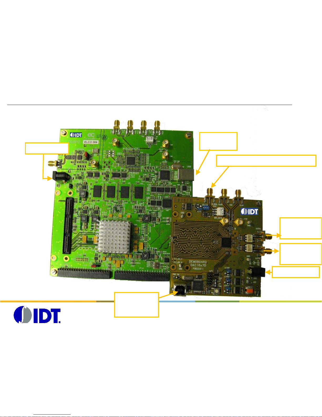
2
CGAP2 board:
Storage and Generat ion of
complex patterns up to
32M (I,Q)- words
DAC1627D board
DAC1627D demoboard+ CGAP2
Board presentation
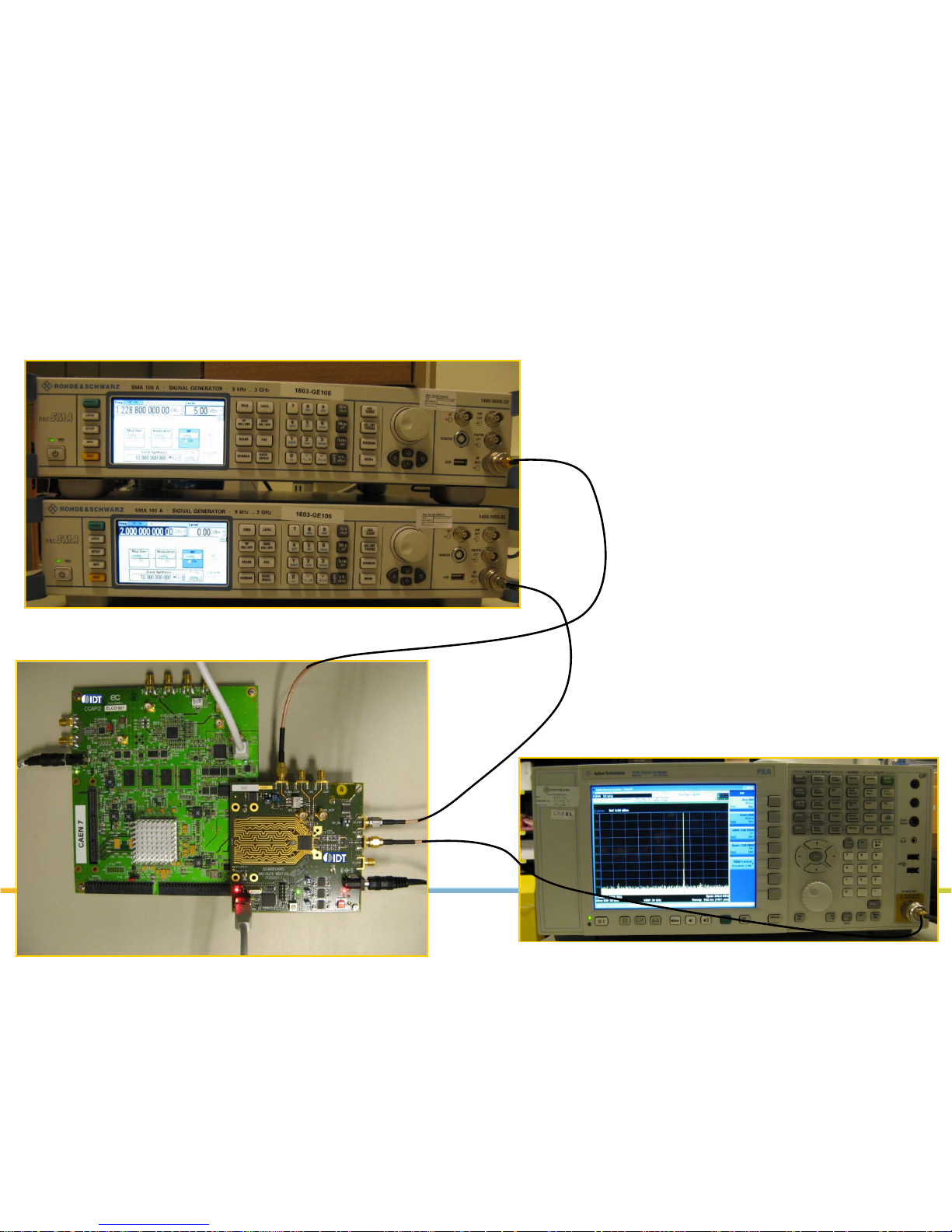
Page 3
3
DAC1627D SPI
USB control
CGAP2 USB
Power 5 Vdc
SMA100A clock generator : DAC clock
Power 5 Vdc
PXA spectrum
analyzer
DAC1627D demoboard+ CGAP2
Board connections
PXA spectrum
analyzer
Page 4
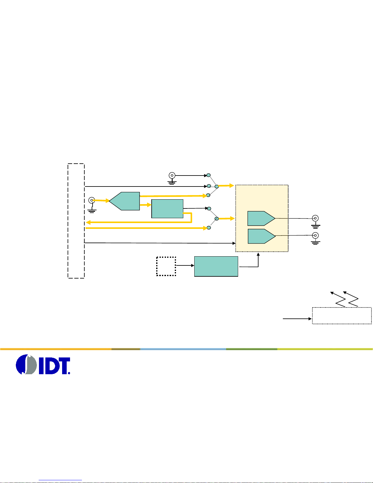
DAC1627 Board overview
Block Diagram
FT2232D
USB<-> SPI
DAC1627
Iout
SPI
DAC clk
USB
con
Data0-13
DAC
6V DC in external
Power Generator
Qout
DAC
CGAP2 QSH connector
SPI
LVDS clk
Divider
/2 /4 /8
splitter
global clk
Iout
Qout
One Global clock is used for both DAC board and CGAP 2 boar d.
This Global Clock is split on two signals:
- one is feeding the DAC1627D
- one is divided and send trough the Samtec connector to the CGAP board to feed the FPGA
Page 5
5
CGAP2 board:
Storage and Generat ion of
complex patterns up to
32M (I,Q)- words
DAC1627D + BGX7100 board
DAC1627D + BGX7100 IQMod demoboard+ CGAP2
Board presentation
Page 6

6
DAC1627D SPI
USB control
CGAP2 USB
Power 5 Vdc
SMB100A clock generator, DAC clock
737.28MHz, 5dBm
Power 6 Vdc
SMA100A clockgen
IQMod clock 2GHz,
0dBm
PXA spectrum
analyzer
DAC1627D + BGX7100 IQMod demoboard+ CGAP2
Board connections
Page 7
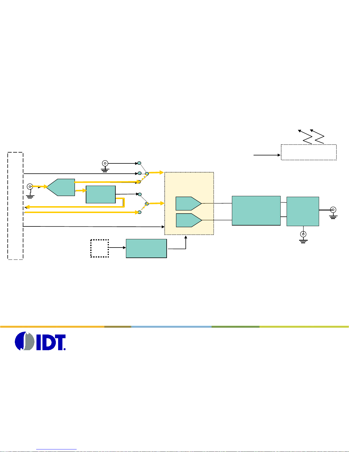
DAC1627/ BGX7100 Board overview
Block Diagram
Low pass Filter
(BW=300Mhz)
FT2232D
USB<-> SPI
DAC1627
Iout
RFout
SPI
DAC clk
USB
con
Data0-13
DAC
6V DC in external
Power Generator
Qout
DAC
External generator
LO Synthe
clock
CGAP2 QSH connector
SPI
LVDS clk
Divider
/2 /4 /8
splitter
BGX7100
AQM
global clock
One Global clock is used for both DAC board and CGAP board.
This Global Clock is split on two signals:
- one is feeding the DAC1627D
- one is divided and send trough the Samtec connector to the CGAP board to feed the FPGA
Page 8

S0/S1/S2 jumpers positi on
8
S0: ON
S1: ON
S2: OFF
S0/S1/S2 jumpers are used to configure the divider ratio for the clock feeding the CGAP board..
For the current software revision, t he ratio value needs to be set to 2.
Please, make sure that the jumpers have the foll owing configuration on the boar d:
Page 9
CLOCKS generation
(Global Clock and LO)
9
Spectrum measurement
Bench overview
Page 10

10
IDT DAC1627 SPI Software
Page 11
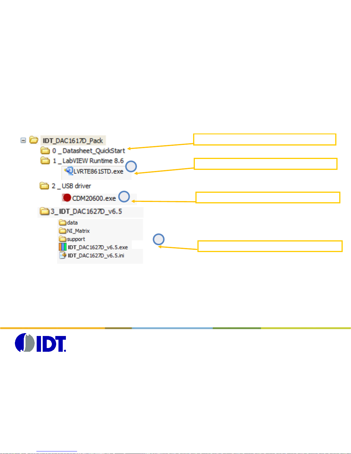
Software Folders
11
Documentations: Datasheets and QuickS tart
LabVIEW Runtime version 8.6
FTDI USB drivers for CGAP and DAC1627 controls
Main Application
3
1
2
To use the IDT_DAC1627D software, the LabVIEW Runtime 8.6 needs to be installed first.
This Runtime could be f ound on the folder named 1_LabVIEW Runtime 8.6.
The driver required t o ac c es s the USB controller on the boar d c ould be found in the folder 2_USB driver
Page 12
CGAP board control panel overview
12
Page 13
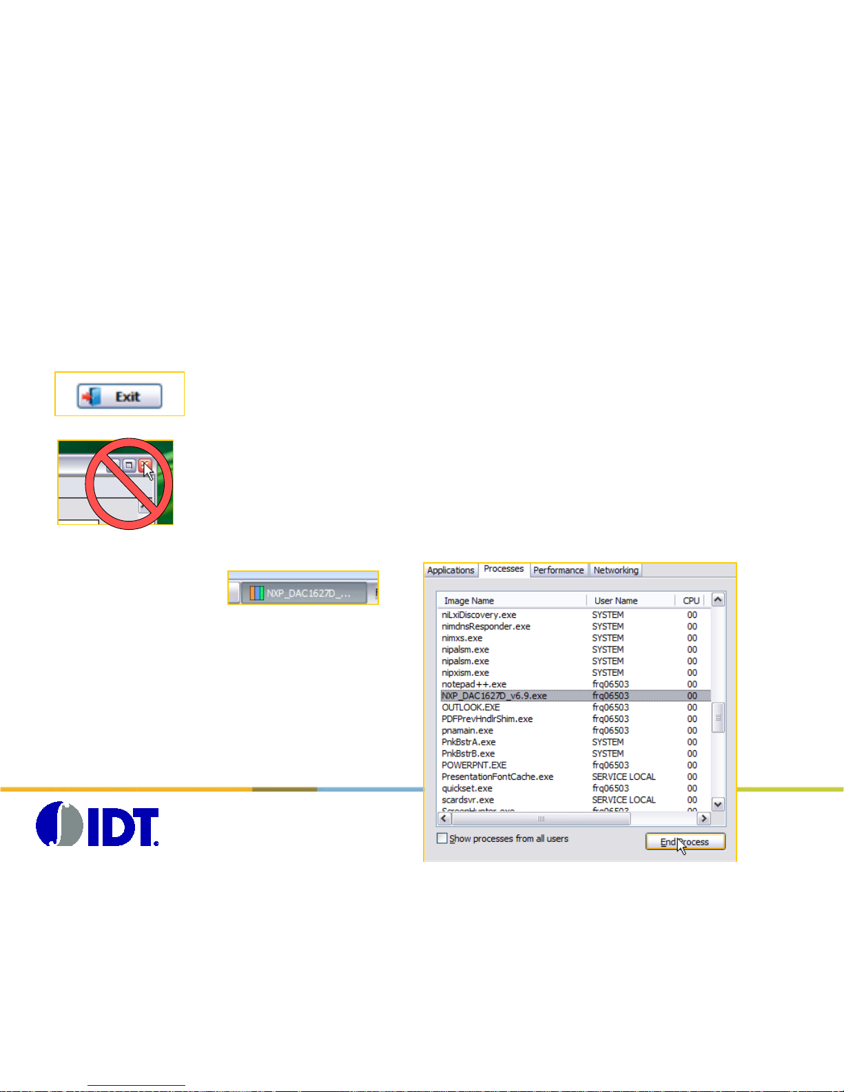
Warning: Exiting the Program
13
When using the IDT DAC1627D SPI Software, some USB connexion are opened
between your laptop/desktop and the boards (CGAP 2 and DA C board).
To prevent any hardwar e is s ue when closing the program
, please use the EXIT
button to close properly the USB connexion.
Do not use the [X] button, otherwise, the U SB c onnexion will still
be alive, and the program won’t be closed properly.
If this happens, the program will be displayed i n t he Windows taskbar, but could not be
accessed anymore.
Please use the Task Manager to End the process:
Page 14
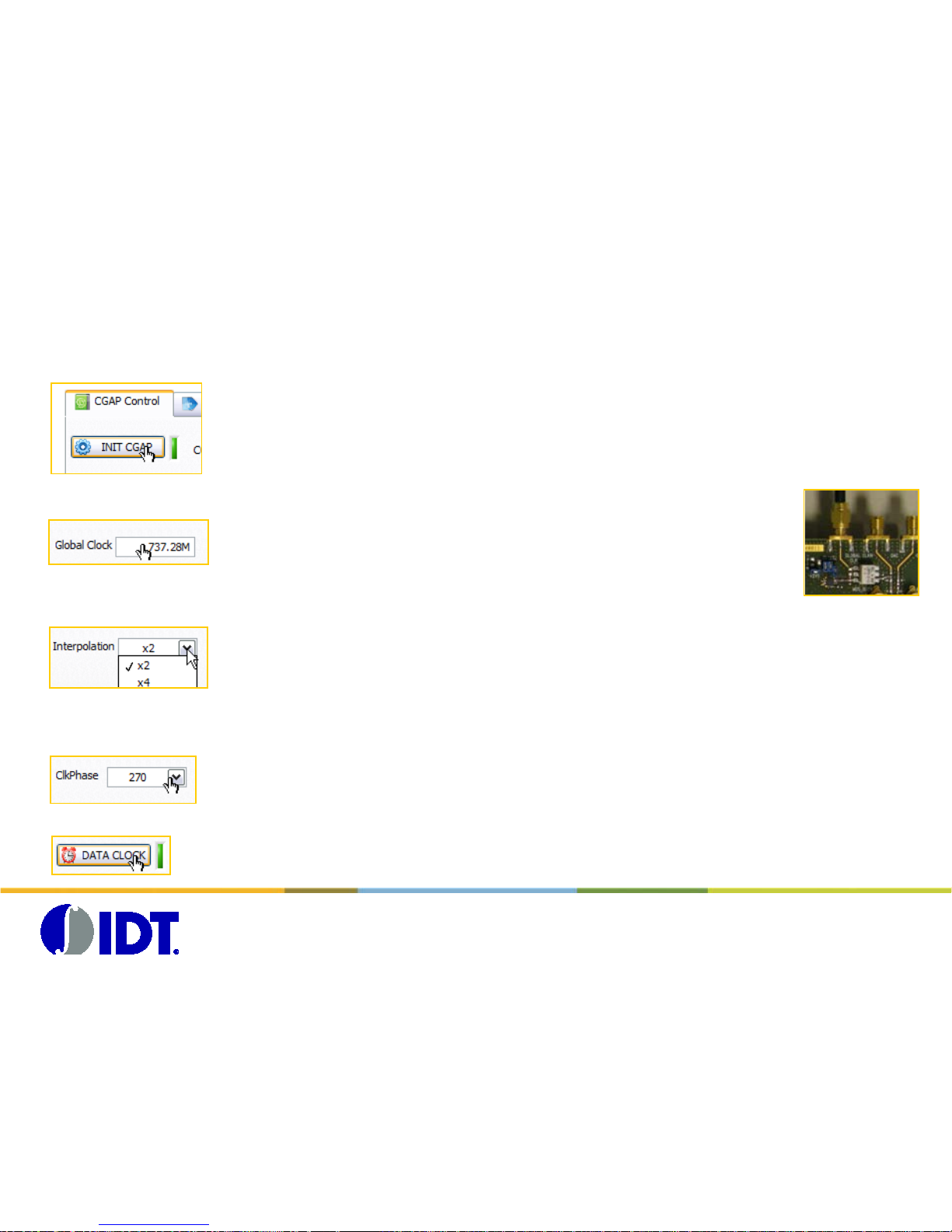
CGAP board start up sequence
14
(1) Initialize the CGAP board USB controller
(2) Specify the Global Clock frequency pr ovided to the DAC board.
(3) Specify the interpolation factor programmed in the DAC1627D.
(4) Specify the clock phase realtionship between the LVDS clock and the
DATA coming from the FPGA.
(5) Press the ‘DATA CLOCK’ button to configure t he CG A P board.
Page 15
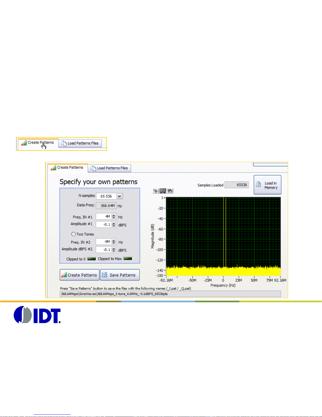
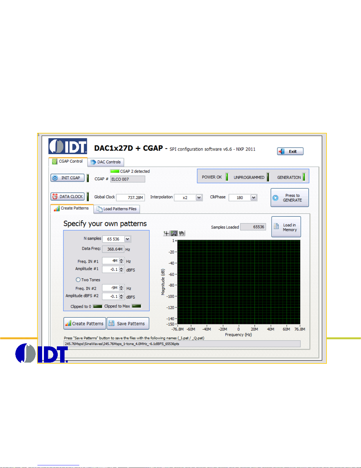
Create Pattern s and program CG AP memories
1/3
15
Select the ‘Create Pattern s’ tab
Page 16

16
Create Pattern s and program CG AP memories
2/3
(a) Select the number N of samples
(b) The Data Frequency is automatically preset fr om the Global clock
value and the interpolation fac t or
(c) Specify the Frequency of the first tone (Hz)
(d) Specify the Amplitude of the f ir s t tone (dBFS)
(e) Click ‘Two T ones’ if needed
(f) Specify the Frequency of the second tone (Hz)
(g) Specify the Amplitude of the sec ond tone (dBFS)
Press ‘Create Patterns’ button to generate the s ignal (I and Q patterns are
generated at the same time)
Press ‘Load in Memory’ button to load the pattern f iles to the CGAP board
memories.
Page 17

17
Create Pattern s and program CG AP memories
3/3
The complex spect rum of the generated si gnal is displayed.
The size of the pat tern indicator is ref r es hed.
The LED indicators diplays the status of the CGAP board (Programmed
and Generation)
The generation of the signal is automatically enabled after t he « Load in
Memory » action.
Page 18

LED Status of the CGAP board
18
When Generation is in pr ogr es s , the
GEN LED is ON (green)
When the clock configuration is correctly
set, the ALIVE LED is blinking (green).
When the ERROR LED is blinking (red),
the clock configuration need to be resent.
Page 19

Load Patterns Files
19
Some patterns are already available with the sof t w ar e.
You need to specify the DATA rate (w) and the type (x) of signals ( Radi o or S ines waves).
Then, I-file and Q-file need to be selected (y).
Press Load in Memory (z) to store the pattern in the FPG A memory
X
Y
W
Z
Y
Page 20

20
Load Patterns and program CGAP memories
In the « patterns » folder, several subfolders are prov ided containing various
pattern types regarding the expected frequency of the DATA signal.
Each subfolder is splitted in two subfolders names Radio and Sinewaves.
The Radio subfolder contains the Radio complex patterns ( WCDMA, GSM, etc).
The Sinewaves subfolder contains the basic s ingl e or dual tones signals.
Any patterns could be added t o this subset, please contact your local AE to know
more about this process.
This structure is r epr es ented in the same way in the GUI.
Page 21

DAC control s panel overview
21
Page 22

DAC control s main features
22
Some SPI settings ar e alr eady available in the
DAC Config boxes.
Select the right one, and Press Load Config
button.
You can reset the device by pressing Reset to
Default button.
You first need to press Re-INIT USB device to
be sure that the PC is able to communicate
with the DAC1617D
All the registers could be read to update the
Graphical User Interface by pressing READ
from the DAC button.
All the registers could be written by pressing
SEND to the DAC button.
On all DAC tab:
When entering each TAB, a self refresh feature is enabled to display the real content of the DAC device.
Page 23

DAC Main Configuration
23
Main parameters of the DAC settings (NCO, interpolation) could be programmed from the Main tab.
Page 24

NCO enable / disable
24
When using the NCO, don’t forget to specify the type of modulation.
Positive or negative refers to the pos ition of the final signal compare to the LO
position after the Iqmod.
Upper and Lower refers to the position of the signal c ompare to the NCO position.
When disabling the NCO, don’t forget to specify no modulation.
Page 25

Interpolat ion f a ctor
25
The interpolation f ac tor need to be specified in two pages .
In the Main tab, please specify the interpolation ratio
In the Data Format / INTR tab, please specify the CDI mode
Please respect t he follwing table :
Interpolation CDI mode
x2 ^2 mode
x4 ^4 mode
x8 ^8 mode
Page 26

DAC digital Adjustement
26
DAC digital tuning tab allows to update digital gain, phas e c or r ec tion, clipping of the I/Q c hannels to help the I/Q balance at
the AQM input.
Page 27

Image Rejection compensati on (experimental)
27
The Image Rejection compensation
window allows to instant aneous ly
update the I/Q gain and the phase
compensation.
Mouse or keyboard inter face could be
use to update the values.
Notice: This feature is experimental for
the moment, and could s how s ome
bugs.
Page 28

DAC analog ad justement
28
DAC analog tuning tab allows to update the analog gain, the auxiliar y DA Cs .
Page 29

Multi Devices S ynchronization
29
MDS tab allows to tune the settings for the multi devices synchronization.
Page 30

LVDS Clock Control
30
LVDS buffer are automatically c al ibr ated with regard to the LVDS clock input.
The tab allows to enable/disable the automatic/manual calibration.
Page 31

Data Input Formatting
31
Interleace/Folded, bit inversions of t he input interface could be set up in t he Data input formatting tab.
Page 32

Test
32
Page 33

Registers
33
All the registers pages could be read and save from t he Regis ters tab.
Page 34

Tools
34
Tools tab allows to see the output spectrum related to the folded image at the DAC output.
Page 35

35
Spectral measurements
How to correctly setup your spectrum analyzer?
Page 36

How to specify the correct settings for the Spectrum analyzer?
36
DAC1627D and BGX7100 provides high end performances, therefore, a correct m easurem ent
setup need to be established to get the real perf orm ances of the dev ic es (and not the bad
performanc es of the spectrum) .
Please refer s to t he Application Not e f r om Agilent to correctly setup the Spectrum.
Same way of working c oul d be used for R&S equipment.
Page 37

37
How to specify the correct settings for the Spectrum analyzer?
Mixer will created second and third
order distorsion if too much power
is send at its input.
Attenuation needs to be correct ly
set up to avoid t he mixer’s
distorsion to occur.
Page 38

38
How to specify the correct settings for the Spectrum analyzer?
You need to find the opti mum mixer levels to
avoid to measure the dis torsion created by the
equipment.
Third order distorsion created by the
Spectrum Analyzer
Second order distorsion created by the
Spectrum Analyzer
Displayed Average Noise Level due to the
Resolution BW
Warning: Please refer to the S pec trum
Analyzer Datasheet to get the real value for
TOI and SHI
Page 39

39
How to specify the correct settings for the Spectrum analyzer?
When measuring Second
harmonic (H 2) , you need t o take
care about the second order
distorsion of the analyzer.
Maximum value that could be measured from
the equipment in this s pec ific settings (RBW).
DANL
(link to RBW)
Second order
distorsion from
the equipment
Warning: Please refer to the S pec trum
Analyzer Datasheet to get the real value for
TOI and SHI
Optimum power level in f r ont of t he mixer.
The attenuation need to be adjusted to fit this
parameter.
Page 40

40
How to specify the correct settings for the Spectrum analyzer?
When measuring Inter-
Modulation product (IMD3) , you
need to take car e about the third
order distorsion of the analyzer.
Maximum value that could be measured from
the equipment in this s pec ific settings (RBW).
DANL
(link to RBW)
Third order
distorsion from
the equipment
Warning: Please refer to the S pec trum
Analyzer Datasheet to get the real value for
TOI and SHI
Optimum power level in f r ont of t he mixer.
The attenuation need to be adjusted to fit this
parameter.
Page 41

41
How to specify the correct settings for the Spectrum analyzer?
You need to find the opti mum mixer levels to avoid
to measure the distors ion created by the equipment.
When measuring a signal of 0dB m power, to avoid to
get H2 coming fr om the S pec trum analyser mixer, a 40dB attenuator level need to be set (it also depends
of the RBW)
If the signal is about -10dBm, then use 30dB of
attenuation to get -10 -30 = -40dBm at the mixer
input.
When measuring Intermodulation pr oduc t (IMD3)
for a -6dBm signal, please us e 22dB at tenuation to
avoid intermodulation product coming fr om the
equipment.
-6-22= -28dBm at the mixer input.
Please update the figur es r egar ding the type of
equipment you are using (cf datasheet of the
equipment).
Page 42

42
Spectral measurements
Understand OIP3 / IMD3 after IQModulator
Page 43

Third Or der Intercept measu r ements
43
Please refers to the Application Note from Agilent for more details.
Page 44

Definition of OIP3
44
In telecommunications, a third-order intercept point (IP3 or TOI) is a measure for nonlinear systems and dev ic es. T he
third-order interc ept point relates nonlinear produc ts caused by the third-order nonlinear term to the linearly amplified
signal, in contrast to the second-order intercept point that uses sec ond or der terms.
Page 45

BGX7100 OIP3
45
OIP3 value is about 26dBm for
2GHz LO frequency
Page 46

Intermodulation see at DAC outputs
46
No intermodulation after
DAC.
Page 47

Intermodulation afte r IQMod (2Ghz)
47
Output Power= -6.33dBm
dBc= -63.12
OIP3=-6.33+63.12/2=25.23dBm
The main contribution for t he
intremodulation is c oming from the IQmod.
Page 48

48
Standard F ilter between
DAC1627D and BGX7100
Page 49

300Mhz Chebychev Filter between DAC1627D and BGX7100
Refers to schematics PCB2227-1.0_17243\DOS_PCB2227-1.0_17243\ PCB2227-1-200-00_1_2.pdf
L101=L104= 39nH , L102=L105: 47nH, L103=L106 = 18nH C165= 10pf C166= 6.8pf
L107=L110= 39nH , L108=L111: 47nH, L109=L112 = 18nH C185= 10pF C186= 6.8pf
49
Page 50

Filter response
50
 Loading...