

Page 1

®
CPS-1848™ User Manual
Titl
Central Packet Switch
Formal Status
June 2, 2014
Page 2

GENERAL DISCLAIMER
Integrated Device Technology, Inc. (“IDT”) reserves the right to make changes to its products or specifications at any time, without notice,
in order to improve design or performance. IDT does not assume responsibility for use of any circuitry described herein other than the
circuitry embodied in an IDT product. Disclosure of the information herein does not convey a license or any other right, by implication or
otherwise, in any patent, trademark, or other intellectual property right of IDT. IDT products may contain errata which can affect product
performance to a minor or immaterial degree. Current characterized errata will be made available upon request. Items identified herein as
“reserved” or “undefined” are reserved for future definition. IDT does not assume responsibility for conflicts or incompatibilities arising
from the future definition of such items. IDT products have not been designed, tested, or manufactured for use in, and thus are not
warranted for, applications where the failure, malfunction, or any inaccuracy in the application carries a risk of death, serious bodily injury ,
or damage to tangible property . Code examples provided herein by IDT are for illustrative purposes only and should not be relied upon for
developing applications. Any use of such code examples shall be at the user's sole risk.
Copyright ©2014 Integrated Device Technology, Inc.
The IDT logo is registered to Integrated Device Technology, Inc.
Page 3

Table of Contents
o
About this Document....................................................................................................................17
Content Summary....................................................................................................................................................................................17
Additional Resources...............................................................................................................................................................................17
Document Conventions and Definitions...................................................................................................................................................17
Device Revision Information....................................................................................................................................................................18
Revision History.......................................................................................................................................................................................18
1. Device Overview...................... .................................................................................................... 23
1.1 Device Description...................................................................................................................................................................................23
1.2 Key Features ...........................................................................................................................................................................................23
1.3 Block Diagrams........................................................................................................................................................................................25
1.4 Typical Applications................................................................................................................................................................................. 26
1.4.1 Wireless Application Benefits...................................................................................................................................................26
1.4.2 Defense and Aerospace Application Benefits.......................................................................................................................... 27
1.4.3 Video and Imaging Application Benefits...................................................................................................................................27
2. RapidIO Por t s .......................... ......................... .......................... .. ......................... .. .................... 28
2.1 Overview..................................................................................................................................................................................................28
2.2 Key Features ...........................................................................................................................................................................................29
2.3 Packet Routing ........................................................................................................................................................................................30
2.3.1 Packet Routing Overview.........................................................................................................................................................30
2.3.2 Unicast Programming Model....................................................................................................................................................31
2.3.3 Multicast Programming Model..................................................................................................................................................33
2.3.4 Programming Examples...........................................................................................................................................................34
2.4 Flow Control.............................................................................................................................................................................................38
2.4.1 Transmitter- and Receiver-Controlled Flow Control Programming Model................................................................................38
2.5 Multicast Event Control Symbols.............................................................................................................................................................39
2.6 Port Reconfiguration Operations..............................................................................................................................................................39
2.6.1 Disabling IDLE2 Operation.......................................................................................................................................................40
2.7 Reset Control Symbol Processing........................................................................................................................................................... 40
2.7.1 Per-Port Reset..........................................................................................................................................................................40
2.7.2 Port Disable/Enable..................................................................................................................................................................42
2.7.3 Generating a Reset Request....................................................................................................................................................42
2.8 Hot Extraction/Insertion............................................................................................................................................................................42
2.8.1 Hot Extraction...........................................................................................................................................................................43
2.8.2 Controlled Removal/Reset........................................................................................................................................................43
2.8.3 Link Partner Insertion............................................................................................................................................................... 48
2.9 Packet Trace and Filtering.......................................................................................................................................................................53
2.9.1 Packet Trace............................................................................................................................................................................53
2.9.2 Packet Filtering.........................................................................................................................................................................57
2.10 Packet Generation and Capture..............................................................................................................................................................57
2.10.1 Packet Generation and Capture Mode Overview.....................................................................................................................58
2.10.2 Packet Generation and Capture Mode Programming Model....................................................................................................59
C
CPS-1848 User Manual 3 June 2, 2014
Formal Status This document is confidential and is subject to an NDA.
Integrated Device Technology
Page 4

Table of Contents
2.11 Packet Transfer Validation and Debug.....................................................................................................................................................62
2.11.1 Overview...................................................................................................................................................................................62
2.11.2 Successful Packet Transfer...................................................................................................................................................... 63
2.11.3 Switch Cannot Accept Packets.................................................................................................................................................63
2.11.4 Switch Is Not Routing Packets Correctly..................................................................................................................................65
2.11.5 Switch Cannot Transmit Packets..............................................................................................................................................66
2.11.6 Requesting Debug Assistance.................................................................................................................................................68
3. RapidIO Lanes ............................................................................................................................. 69
3.1 Lane to Port Mapping ..............................................................................................................................................................................70
3.2 Lane and Port Speeds.............................................................................................................................................................................73
3.2.1 Lane Speed Change Examples................................................................................................................................................73
3.3 Lane, PLL, and Port Power-Down...........................................................................................................................................................75
3.4 Port and Lane Initialization Sequence.....................................................................................................................................................75
3.4.1 Signal Quality Optimization......................................................................................................................................................76
3.5 Loopback Capabilities..............................................................................................................................................................................82
3.5.1 Lane Loopback Modes.............................................................................................................................................................83
3.5.2 Port Loopback Mode................................................................................................................................................................ 83
3.6 Bit Error Rate Testing...............................................................................................................................................................................84
3.6.1 PRBS Polynomials...................................................................................................................................................................84
3.6.2 User-Defined Patterns..............................................................................................................................................................84
3.6.3 PRBS Pattern Generator..........................................................................................................................................................85
3.6.4 PRBS Pattern Checker and Log (Revision C)..........................................................................................................................85
4. Switch Fabric............................................................................................................................... 87
4.1 Key Features ...........................................................................................................................................................................................87
4.2 Switch Fabric Architecture.......................................................................................................................................................................88
4.3 Input Buffer..............................................................................................................................................................................................89
4.4 Input Buffer to Crosspoint Buffer Transfers..............................................................................................................................................89
4.4.1 VoQ Fairness/Starvation Avoidance.........................................................................................................................................90
4.4.2 Multicast Packets......................................................................................................................................................................90
4.5 Crosspoint Buffers...................................................................................................................................................................................90
4.6 Crosspoint Buffer to Final Buffer Transfers..............................................................................................................................................91
4.7 Maintenance Transaction Support...........................................................................................................................................................91
4.8 Final Buffer...............................................................................................................................................................................................92
5. Performance ................................................................................................................................ 93
5.1 Overview..................................................................................................................................................................................................93
5.1.1 Throughput...............................................................................................................................................................................93
5.1.2 Latency.....................................................................................................................................................................................93
5.1.3 Latency Variation...................................................................................................................................................................... 94
5.2 Performance Monitoring...........................................................................................................................................................................94
5.2.1 Traffic Efficiency.......................................................................................................................................................................95
5.2.2 Congestion Detection...............................................................................................................................................................95
5.2.3 Resetting Performance Registers.............................................................................................................................................95
5.3 Performance Measurements....................................................................................................................................................................96
5.3.1 Buffer Management Settings....................................................................................................................................................96
5.3.2 Store-and-Forward or Cut-Through Mode................................................................................................................................98
5.3.3 Transmitter-Controlled or Receiver-Controlled Flow Control Mode..........................................................
................................98
5.4 Port-to-Port Performance Characteristics................................................................................................................................................99
5.4.1 Packet Latency Performance................................................................................................................................................... 99
CPS-1848 User Manual 4 June 2, 2014
Formal Status This document is confidential and is subject to an NDA.
Integrated Device Technology
Page 5

Table of Contents
5.4.2 Packet Throughput Performance............................................................................................................................................100
5.4.3 Multicast Latency Performance..............................................................................................................................................102
5.4.4 Multicast Throughput Performance........................................................................................................................................ 102
5.4.5 Multicast-Event Control Symbol (MECS) Latency..................................................................................................................103
6. Event Management. .. .. .. ............................ .. ........................... ... ........................... ...................... 104
6.1 Event Management Overview................................................................................................................................................................104
6.1.1 Logical/Transport Layer Events Overview..............................................................................................................................108
6.1.2 Physical Layer Error Management Overview.........................................................................................................................109
6.1.3 Lane Error Management Overview..........................................................................................................................................111
6.1.4 I2C Error Management Overview............................................................................................................................................112
6.1.5 Configuration Error Management Overview............................................................................................................................113
6.2 Event Detection ......................................................................................................................................................................................113
6.2.1 Logical and Transport Layer Events........................................................................................................................................113
6.2.2 Physical Layer Events.............................................................................................................................................................115
6.2.3 Lane Events............................................................................................................................................................................124
6.2.4 I2C Events..............................................................................................................................................................................126
6.2.5 JTAG Events (Revision A/B Only).......................................................................................................................................... 126
6.2.6 Configuration Block Events.................................................................................................................................................... 127
6.2.7 Trace and Filter Events..........................................................................................................................................................127
6.2.8 Packet Generation and Capture Mode Events.......................................................................................................................127
6.2.9 Error Log Events.....................................................................................................................................................................127
6.3 Event Notification...................................................................................................................................................................................137
6.3.1 Logical Layer Events Notification........................................................................................................................................... 137
6.3.2 Physical Layer Events Notification.........................................................................................................................................139
6.3.3 Lane Event Notification...........................................................................................................................................................146
6.3.4 I2C Event Notification.............................................................................................................................................................146
6.3.5 JTAG 1149.1 Event Notification (Revision A/B Only).............................................................................................................147
6.3.6 Configuration Block Event Notification...................................................................................................................................147
6.3.7 Trace and Filter Event Notification.........................................................................................................................................147
6.3.8 Packet Generation and Capture Mode Event Notification......................................................................................................147
6.3.9 Port-Write Formats, Programming Model, and Generation....................................................................................................148
6.3.10 Interrupt Notification...............................................................................................................................................................152
6.3.11 Error Log Event Notification Programming Model..................................................................................................................152
6.4 Event Isolation.......................................................................................................................................................................................154
6.4.1 Fatal Link Response Timeout Isolation..................................................................................................................................156
6.4.2 Received Retry Count Trigger Congestion Isolation ..............................................................................................................157
6.4.3 TTL Event Isolation.................................................................................................................................................................157
6.4.4 Transmit Packet Dropped via CRC Retransmit Limit Isolation...............................................................................................157
6.4.5 Packet Received With a CRC Error While CRC Error Suppression Enabled Isolation..........................................................157
6.4.6 Software Controlled Isolation Functions.................................................................................................................................158
6.5 Event Clearing and Recovery................................................................................................................................................................ 158
6.5.1 Logical Layer Event Clearing and Handling........................................................................................................................... 158
6.5.2 Physical Layer Events Clearing and Handling........................................................................................................................159
6.5.3 Lane Event Clearing and Handling......................................................................................................................................... 167
6.5.4 I2C Event Clearing and Handling...........................................................................................................................................167
6.5.5 JTAG 1149.1 Events (Revision A/B Only)..............................................................................................................................168
6.5.6 Configuration Block Events....................................................................................................................................................168
6.5.7 Trace, Filter, and PGC Events................................................................................................................................................169
CPS-1848 User Manual 5 June 2, 2014
Formal Status This document is confidential and is subject to an NDA.
Integrated Device Technology
Page 6

Table of Contents
7. I2C Interface.............................................................................................................................. 170
7.1 Overview................................................................................................................................................................................................170
7.2 Master/Slave Configuration....................................................................................................................................................................170
7.3 Temporary Master Mode........................................................................................................................................................................ 170
7.3.1 Obtaining Configuration in Master Mode................................................................................................................................171
7.3.2 Commanded Master Mode.....................................................................................................................................................171
7.3.3 Master Clock Frequency.........................................................................................................................................................171
7.3.4 EEPROM Format....................................................................................................................................................................171
7.3.5 CRC Calculation.....................................................................................................................................................................173
7.3.6 Register Map Example...........................................................................................................................................................175
7.3.7 EEPROM Format Example.....................................................................................................................................................175
7.3.8 I2C Master Mode Validation Debug........................................................................................................................................176
7.4 Slave Mode............................................................................................................................................................................................177
7.4.1 Signaling in Slave Mode.........................................................................................................................................................177
7.4.2 Connecting to Standard-, Fast-, and Hs-Mode Devices as a Slave.......................................................................................180
7.4.3 CPS-1848 Memory Access through I2C as a Slave...............................................................................................................180
8. JTAG and Boundary Scan.......................................................................................................... 183
8.1 Overview................................................................................................................................................................................................183
8.2 JTAG and AC Extest Compliance..........................................................................................................................................................183
8.3 Test Instructions.....................................................................................................................................................................................184
8.4 Device ID Register.................................................................................................................................................................................184
8.5 Initialization and Reset...........................................................................................................................................................................185
8.6 Configuration Register Access (Revision A/B).......................................................................................................................................185
8.6.1 Configuration Register Access – Writes.................................................................................................................................186
8.6.2 Configuration Register Access – Reads................................................................................................................................. 186
8.7 Configuration Register Access (Revision C).......................................................................................................................................... 187
8.7.1 Inter-Command Delay............................................................................................................................................................188
8.7.2 Configuration Register Access – Writes.................................................................................................................................190
8.7.3 Configuration Register Access – Reads................................................................................................................................. 190
8.8 JTAG Clock Constraints.........................................................................................................................................................................191
8.9 Boundary Scan......................................................................................................................................................................................191
9. Reset and Initialization ............................................................................................................. 192
9.1 Hardware Reset.....................................................................................................................................................................................192
9.1.1 Power-Up Reset.....................................................................................................................................................................192
9.1.2 Resets after Power-Up...........................................................................................................................................................192
9.2 Initialization............................................................................................................................................................................................ 193
9.2.1 I2C Initialization......................................................................................................................................................................193
9.2.2 Link Initialization.....................................................................................................................................................................193
9.2.3 Register Initialization..............................................................................................................................................................194
9.2.4 Computing Timeout Values....................................................................................................................................................195
10. Registers ................................................................................................................................... 197
10.1 Overview................................................................................................................................................................................................197
10.1.1 RapidIO Compliance..............................................................................................................................................................197
10.1.2 Interpretation of Reserved Register Bits.................................................................................................................................198
10.1.3 Backward Compatibility..........................................................................................................................................................198
10.1.4 Register Type Field Definitions...............................................................................................................................................198
10.2 Address Map..........................................................................................................................................................................................198
CPS-1848 User Manual 6 June 2, 2014
Formal Status This document is confidential and is subject to an NDA.
Integrated Device Technology
Page 7

Table of Contents
10.3 RapidIO Capability Registers (CARs)....................................................................................................................................................212
10.3.1 Device Identity CAR...............................................................................................................................................................212
10.3.2 Device Information CAR.........................................................................................................................................................213
10.3.3 Assembly Identity CAR........................................................................................................................................................... 214
10.3.4 Assembly Information CAR....................................................................................................................................................214
10.3.5 Processing Element Features CAR........................................................................................................................................ 215
10.3.6 Switch Port Information CAR.................................................................................................................................................. 217
10.3.7 Source Operations CAR.........................................................................................................................................................218
10.3.8 Switch Multicast Support CAR................................................................................................................................................219
10.3.9 Switch Route Table Entries Table Limit CAR..........................................................................................................................220
10.3.10 Switch Multicast Information CAR..........................................................................................................................................221
10.4 RapidIO Control and Status Registers (CSRs)......................................................................................................................................222
10.4.1 Host Base deviceID Lock CSR............................................................................................................................................... 222
10.4.2 Component Tag CSR..............................................................................................................................................................222
10.4.3 Standard Route Table Entries Configuration destID Select CSR...........................................................................................223
10.4.4 Standard Route Table Entry Configuration Port Select CSR..................................................................................................224
10.4.5 Standard Route Table Entry Default Port CSR....................................................................................................................... 225
10.4.6 Multicast Mask Port CSR........................................................................................................................................................226
10.4.7 Multicast Association Selection CSR......................................................................................................................................227
10.4.8 Multicast Association Operations CSR................................................................................................................................... 228
10.5 LP-Serial Extended Features Registers with Software Assisted Error Recovery..................................................................................229
10.5.1 Port Maintenance Block Header Register..............................................................................................................................229
10.5.2 Port Link Timeout Control CSR..............................................................................................................................................230
10.5.3 Port General Control CSR......................................................................................................................................................230
10.5.4 Port {0..17} S-RIO Extended Features Base Addresses........................................................................................................231
10.5.5 Port {0..17} Link Maintenance Request CSR.........................................................................................................................232
10.5.6 Port {0..17} Link Maintenance Response CSR.......................................................................................................................233
10.5.7 Port {0..17} Local ackID CSR.................................................................................................................................................234
10.5.8 Port {0..17} Error and Status CSR.......................................................................................................................................... 235
10.5.9 Port {0..17} Control 1 CSR.....................................................................................................................................................238
10.5.10 Port {0..17} Control 2 CSR.....................................................................................................................................................242
10.6 Virtual Channel Extended Features Block Registers.............................................................................................................................244
10.6.1 VC Register Block Header Register.......................................................................................................................................244
10.7 Error Management Extensions Block Registers....................................................................................................................................245
10.7.1 Error Management Extensions Block Header Register..........................................................................................................245
10.7.2 Logical/Transport Layer Error Detect CSR............................................................................................................................. 246
10.7.3 Logical/Transport Layer Error Enable CSR............................................................................................................................247
10.7.4 Logical/Transport Layer deviceID Capture CSR....................................................................................................................248
10.7.5 Logical/Transport Layer Control Capture CSR....................................................................................................................... 249
10.7.6 Port-Write Target deviceID CSR.............................................................................................................................................251
10.7.7 Packet Time to Live CSR.......................................................................................................................................................252
10.7.8 Port Error Management Register Base Addresses................................................................................................................253
10.7.9 Port {0..17} Error Detect CSR.................................................................................................................................................254
10.7.10 Port {0..17} Error Rate Enable CSR.......................................................................................................................................256
10.7.11 Port {0..17} Attributes Capture CSR.......................................................................................................................................258
10.7.12 Port {0..17} Capture 0 CSR....................................................................................................................................................259
10.7.13 Port {0..17} Capture 1 CSR....................................................................................................................................................260
10.7.14 Port {0..17} Capture 2 CSR....................................................................................................................................................260
10.7.15 Port {0..17} Capture 3 CSR....................................................................................................................................................261
10.7.16 Port {0..17} Error Rate CSR...................................................................................................................................................262
CPS-1848 User Manual 7 June 2, 2014
Formal Status This document is confidential and is subject to an NDA.
Integrated Device Technology
Page 8

Table of Contents
10.7.17 Port {0..17} Error Rate Threshold CSR..................................................................................................................................264
10.8 Lane Status Registers ........................................................................................................................................................................... 265
10.8.1 Lane {0..47} Status Base Addresses...................................................................................................................................... 265
10.8.2 Lane Status Block Header Register.......................................................................................................................................267
10.8.3 Lane {0..47} Status 0 CSR.....................................................................................................................................................268
10.8.4 Lane {0..47} Status 1 CSR.....................................................................................................................................................270
10.8.5 Lane {0..47} Status 2 CSR.....................................................................................................................................................272
10.8.6 Lane {0..47} Status 3 CSR.....................................................................................................................................................273
10.8.7 Lane {0..47} Status 4 CSR.....................................................................................................................................................275
10.9 IDT Specific Miscellaneous Registers....................................................................................................................................................276
10.9.1 Route Port Select Register.....................................................................................................................................................276
10.9.2 Multicast Route Select Register.............................................................................................................................................277
10.9.3 Port n Watermarks Base Addresses......................................................................................................................................278
10.9.4 Port {0..17} Watermarks Register........................................................................................................................................... 279
10.9.5 Broadcast Watermarks Register.............................................................................................................................................280
10.10 IDT Specific Event Notification Control Registers..................................................................................................................................281
10.10.1 Aux Port Error Capture Enable Register................................................................................................................................281
10.10.2 Aux Port Error Detect Register...............................................................................................................................................282
10.10.3 Configuration Block Error Capture Enable Register...............................................................................................................283
10.10.4 Configuration Block Error Detect Register..............................................................................................................................284
10.10.5 Impl. Specific Logical/Transport Layer Address Capture Register......................................................................................... 286
10.10.6 Logical/Transport Layer Error Report Enable Register...........................................................................................................287
10.10.7 Port {0..17} Error Report Enable Base Addresses.................................................................................................................288
10.10.8 Port {0..17} Error Report Enable Register..............................................................................................................................289
10.10.9 Port {0..17} Implementation Specific Error Report Enable Register.......................................................................................291
10.10.10 Broadcast Port Error Report Enable Register........................................................................................................................ 294
10.10.11 Broadcast Port Implementation Specific Error Report Enable Register.................................................................................296
10.10.12 Lane n Error Report Enable Base Addresses........................................................................................................................ 298
10.10.13 Lane {0..47} Error Report Enable Register.............................................................................................................................300
10.10.14 Broadcast Lane Error Report Enable Register.......................................................................................................................301
10.11 Packet Generation and Capture Registers............................................................................................................................................302
10.11.1 Packet Generation and Capture Base Addresses.................................................................................................................. 302
10.11.2 Port {0..17} Packet Generation and Capture Mode Configuration Register...........................................................................303
10.11.3 Port {0..17} Packet Generation and Capture Mode Data Register......................................................................................... 304
10.12 IDT Specific Routing Table Registers....................................................................................................................................................305
10.12.1 Base Addresses for IDT Specific Routing Table Registers.....................................................................................................305
10.12.2 Broadcast Device Route Table Register {0..255}...................................................................................................................306
10.12.3 Broadcast Domain Route Table Register {0..255}..................................................................................................................307
10.12.4 Port {0..17} Device Route Table Register {0..255}..................................................................................................................308
10.12.5 Port {0..17} Domain Routing Table Register {0..255}.............................................................................................................309
10.13 Trace Comparison Values and Masks Registers...................................................................................................................................310
10.13.1 Base Addresses for Trace Comparison Values and Masks Registers...................................................................................310
10.13.2 Port {0..17} Trace 0 Value 0 Register......................................................................................................................................311
10.13.3 Port {0..17} Trace 0 Value 1 Register......................................................................................................................................311
10.13.4 Port {0..17} Trace 0 Value 2 Register..................................................................................................................................... 312
10.13.5 Port {0..17} Trace 0 Value 3 Register..................................................................................................................................... 312
10.13.6 Port {0..17} Trace 0 Value 4 Register..................................................................................................................................... 313
10.13.7 Port {0..17} Trace 0 Mask 0 Register.....................................................................................................................................313
10.13.8 Port {0..17} Trace 0 Mask 1 Register.....................................................................................................................................314
10.13.9 Port {0..17} Trace 0 Mask 2 Register.....................................................................................................................................314
CPS-1848 User Manual 8 June 2, 2014
Formal Status This document is confidential and is subject to an NDA.
Integrated Device Technology
Page 9

Table of Contents
10.13.10 Port {0..17} Trace 0 Mask 3 Register.....................................................................................................................................315
10.13.11 Port {0..17} Trace 0 Mask 4 Register.....................................................................................................................................315
10.13.12 Port {0..17} Trace 1 Value 0 Register.....................................................................................................................................316
10.13.13 Port {0..17} Trace 1 Value 1 Register.....................................................................................................................................316
10.13.14 Port {0..17} Trace 1 Value 2 Register.....................................................................................................................................317
10.13.15 Port {0..17} Trace 1 Value 3 Register.....................................................................................................................................317
10.13.16 Port {0..17} Trace 1 Value 4 Register.....................................................................................................................................318
10.13.17 Port {0..17} Trace 1 Mask 0 Register.....................................................................................................................................318
10.13.18 Port {0..17} Trace 1 Mask 1 Register.....................................................................................................................................319
10.13.19 Port {0..17} Trace 1 Mask 2 Register.....................................................................................................................................319
10.13.20 Port {0..17} Trace 1 Mask 3 Register.....................................................................................................................................320
10.13.21 Port {0..17} Trace 1 Mask 4 Register.....................................................................................................................................320
10.13.22 Port {0..17} Trace 2 Value 0 Register.....................................................................................................................................321
10.13.23 Port {0..17} Trace 2 Value 1 Register.....................................................................................................................................321
10.13.24 Port {0..17} Trace 2 Value 2 Register.....................................................................................................................................322
10.13.25 Port {0..17} Trace 2 Value 3 Register.....................................................................................................................................322
10.13.26 Port {0..17} Trace 2 Value 4 Register.....................................................................................................................................323
10.13.27 Port {0..17} Trace 2 Mask 0 Register.....................................................................................................................................323
10.13.28 Port {0..17} Trace 2 Mask 1 Register.....................................................................................................................................324
10.13.29 Port {0..17} Trace 2 Mask 2 Register.....................................................................................................................................324
10.13.30 Port {0..17} Trace 2 Mask 3 Register.....................................................................................................................................325
10.13.31 Port {0..17} Trace 2 Mask 4 Register.....................................................................................................................................325
10.13.32 Port {0..17} Trace 3 Value 0 Register.....................................................................................................................................326
10.13.33 Port {0..17} Trace 3 Value 1 Register.....................................................................................................................................326
10.13.34 Port {0..17} Trace 3 Value 2 Register.....................................................................................................................................327
10.13.35 Port {0..17} Trace 3 Value 3 Register.....................................................................................................................................327
10.13.36 Port {0..17} Trace 3 Value 4 Register.....................................................................................................................................328
10.13.37 Port {0..17} Trace 3 Mask 0 Register.....................................................................................................................................328
10.13.38 Port {0..17} Trace 3 Mask 1 Register.....................................................................................................................................329
10.13.39 Port {0..17} Trace 3 Mask 2 Register.....................................................................................................................................329
10.13.40 Port {0..17} Trace 3 Mask 3 Register.....................................................................................................................................330
10.13.41 Port {0..17} Trace 3 Mask 4 Register.....................................................................................................................................330
10.13.42 Broadcast Trace 0 Value 0 Register.......................................................................................................................................331
10.13.43 Broadcast Trace 0 Value 1 Register.......................................................................................................................................331
10.13.44 Broadcast Trace 0 Value 2 Register.......................................................................................................................................332
10.13.45 Broadcast Trace 0 Value 3 Register.......................................................................................................................................332
10.13.46 Broadcast Trace 0 Value 4 Register.......................................................................................................................................333
10.13.47 Broadcast Trace 0 Mask 0 Register.......................................................................................................................................333
10.13.48 Broadcast Trace 0 Mask 1 Register.......................................................................................................................................334
10.13.49 Broadcast Trace 0 Mask 2 Register.......................................................................................................................................334
10.13.50 Broadcast Trace 0 Mask 3 Register.......................................................................................................................................335
10.13.51 Broadcast Trace 0 Mask 4 Register.......................................................................................................................................335
10.13.52 Broadcast Trace 1 Value 0 Register.......................................................................................................................................336
10.13.53 Broadcast Trace 1 Value 1 Register.......................................................................................................................................336
10.13.54 Broadcast Trace 1 Value 2 Register.......................................................................................................................................337
10.13.55 Broadcast Trace 1 Value 3 Register.......................................................................................................................................337
10.13.56 Broadcast Trace 1 Value 4 Register.......................................................................................................................................338
10.13.57 Broadcast Trace 1 Mask 0 Register.......................................................................................................................................338
10.13.58 Broadcast Trace 1 Mask 1 Register.......................................................................................................................................339
10.13.59 Broadcast Trace 1 Mask 2 Register.....................................................................................
..................................................339
CPS-1848 User Manual 9 June 2, 2014
Formal Status This document is confidential and is subject to an NDA.
Integrated Device Technology
Page 10

Table of Contents
10.13.60 Broadcast Trace 1 Mask 3 Register.......................................................................................................................................340
10.13.61 Broadcast Trace 1 Mask 4 Register.......................................................................................................................................340
10.13.62 Broadcast Trace 2 Value 0 Register.......................................................................................................................................341
10.13.63 Broadcast Trace 2 Value 1 Register.......................................................................................................................................341
10.13.64 Broadcast Trace 2 Value 2 Register.......................................................................................................................................342
10.13.65 Broadcast Trace 2 Value 3 Register.......................................................................................................................................342
10.13.66 Broadcast Trace 2 Value 4 Register.......................................................................................................................................343
10.13.67 Broadcast Trace 2 Mask 0 Register.......................................................................................................................................343
10.13.68 Broadcast Trace 2 Mask 1 Register.......................................................................................................................................344
10.13.69 Broadcast Trace 2 Mask 2 Register.......................................................................................................................................344
10.13.70 Broadcast Trace 2 Mask 3 Register.......................................................................................................................................345
10.13.71 Broadcast Trace 2 Mask 4 Register.......................................................................................................................................345
10.13.72 Broadcast Trace 3 Value 0 Register.......................................................................................................................................346
10.13.73 Broadcast Trace 3 Value 1 Register.......................................................................................................................................346
10.13.74 Broadcast Trace 3 Value 2 Register.......................................................................................................................................347
10.13.75 Broadcast Trace 3 Value 3 Register.......................................................................................................................................347
10.13.76 Broadcast Trace 3 Value 4 Register.......................................................................................................................................348
10.13.77 Broadcast Trace 3 Mask 0 Register.......................................................................................................................................348
10.13.78 Broadcast Trace 3 Mask 1 Register.......................................................................................................................................349
10.13.79 Broadcast Trace 3 Mask 2 Register.......................................................................................................................................349
10.13.80 Broadcast Trace 3 Mask 3 Register.......................................................................................................................................350
10.13.81 Broadcast Trace 3 Mask 4 Register.......................................................................................................................................350
10.14 Global Device Configuration Registers..................................................................................................................................................351
10.14.1 Device Control 1 Register.......................................................................................................................................................351
10.14.2 Configuration Block Error Report Register.............................................................................................................................353
10.14.3 Aux Port Error Report Enable Register..................................................................................................................................354
10.14.4 RapidIO Domain Register.......................................................................................................................................................355
10.14.5 Port-Write Control Register....................................................................................................................................................356
10.14.6 RapidIO Assembly Identification CAR Override.....................................................................................................................357
10.14.7 RapidIO Assembly Information CAR Override....................................................................................................................... 357
10.14.8 Device Soft Reset Register....................................................................................................................................................358
10.14.9 I2C Master Control Register...................................................................................................................................................358
10.14.10 I2C Master Status and Control Register ................................................................................................................................. 360
10.14.11 JTAG Control Register (Revision A/B)....................................................................................................................................361
10.14.12 External MCES Trigger Counter Register..............................................................................................................................362
10.14.13 Maintenance Dropped Packet Counter Register....................................................................................................................362
10.14.14 Switch Parameters 1 Register................................................................................................................................................363
10.14.15 Switch Parameters 2 Register................................................................................................................................................365
10.14.16 Quadrant Configuration Register............................................................................................................................................ 366
10.14.17 Device Reset and Control Register........................................................................................................................................368
10.15 Implementation Specific Multicast Mask Registers................................................................................................................................369
10.15.1 Implementation Specific Multicast Mask Base Addresses.....................................................................................................369
10.15.2 Broadcast Multicast Mask Register {0..39}............................................................................................................................. 370
10.15.3 Port {0..17} Multicast Mask Register {0..39}...........................................................................................................................371
10.16 Port Function Registers.........................................................................................................................................................................372
10.16.1 Port {0..17} Function Registers Base Addresses...................................................................................................................372
10.16.2 Port {0..17} Operations Register.............................................................................................................................................373
10.16.3 Port {0..17} Implementation Specific Error Detect Register....................................................................................................376
10.16.4 Port {0..17} Implementation Specific Error Rate Enable Register........................................................
..................................379
10.16.5 Port {0..17} VC0 Acknowledgements Transmitted Counter Register.....................................................................................382
CPS-1848 User Manual 10 June 2, 2014
Formal Status This document is confidential and is subject to an NDA.
Integrated Device Technology
Page 11

Table of Contents
10.16.6 Port {0..17} Not Acknowledgements Transmitted Counter Register.......................................................................................382
10.16.7 Port {0..17} VC0 Retry Symbols Transmitted Counter Register............................................................................................. 383
10.16.8 Port {0..17} VC0 Packets Transmitted Counter Register........................................................................................................383
10.16.9 Port {0..17} Trace Match Counter Value 0 Register................................................................................................................384
10.16.10 Port {0..17} Trace Match Counter Value 1 Register................................................................................................................384
10.16.11 Port {0..17} Trace Match Counter Value 2 Register................................................................................................................385
10.16.12 Port {0..17} Trace Match Counter Value 3 Register................................................................................................................385
10.16.13 Port {0..17} Filter Match Counter Value 0 Register.................................................................................................................386
10.16.14 Port {0..17} Filter Match Counter Value 1 Register.................................................................................................................386
10.16.15 Port {0..17} Filter Match Counter Value 2 Register.................................................................................................................387
10.16.16 Port {0..17} Filter Match Counter Value 3 Register.................................................................................................................387
10.16.17 Port {0..17} VC0 Acknowledgements Received Counter Register.........................................................................................388
10.16.18 Port {0..17} Not Acknowledgements Received Counter Register...........................................................................................388
10.16.19 Port {0..17} VC0 Retry Symbols Received Counter Register................................................................................................. 389
10.16.20 Port {0..17} VC0 Switch Crosspoint Buffer Output Packet Counter Register.........................................................................389
10.16.21 Port {0..17} VC0 Packets Received Counter Register............................................................................................................390
10.16.22 Port {0..17} Trace Port-Write Reset Register..........................................................................................................................391
10.16.23 Port {0..17} Lane Synchronization Register............................................................................................................................392
10.16.24 Port {0..17} VC0 Received Packets Dropped Counter Register.............................................................................................393
10.16.25 Port {0..17} VC0 Transmitted Packets Dropped Counter Register.........................................................................................394
10.16.26 Port {0..17} VC0 TTL Packets Dropped Counter Register..................................................................................................... 395
10.16.27 Port {0..17} VC0 CRC Limit Packets Dropped Counter Register........................................................................................... 395
10.16.28 Port {0..17} Congestion Retry Counter Register.....................................................................................................................396
10.16.29 Port {0..17} Status and Control Register................................................................................................................................397
10.16.30 Broadcast Port Operations Register....................................................................................................................................... 398
10.16.31 Broadcast Port Implementation Specific Error Detect Register.............................................................................................. 401
10.16.32 Broadcast Port Implementation Specific Error Rate Enable Register....................................................................................404
10.17 Implementation Specific Error Logging Registers.................................................................................................................................. 407
10.17.1 Error Log Register..................................................................................................................................................................407
10.17.2 Error Log Data Register..........................................................................................................................................................408
10.18 Special Error Registers..........................................................................................................................................................................408
10.18.1 Special Error Registers Base Addresses...............................................................................................................................408
10.18.2 Error Log Match Register {0..7}..............................................................................................................................................409
10.18.3 Error Log Match Status Register............................................................................................................................................410
10.18.4 Error Log Events Register.......................................................................................................................................................411
10.18.5 Error Log Control 2 Register...................................................................................................................................................412
10.19 PLL Registers........................................................................................................................................................................................413
10.19.1 PLL Register Base Addresses................................................................................................................................................413
10.19.2 PLL {0..11} Control 1 Register................................................................................................................................................414
10.19.3 PLL {0..11} Control 2 Register................................................................................................................................................415
10.19.4 Broadcast PLL Control Register.............................................................................................................................................416
10.20 Lane Control Registers..........................................................................................................................................................................417
10.20.1 Lane Control Base Addresses................................................................................................................................................ 417
10.20.2 Lane {0..47} Control Register.................................................................................................................................................419
10.20.3 Lane {0..47} PRBS Generator Seed Register........................................................................................................................423
10.20.4 Lane {0..47} PRBS Error Counter Register............................................................................................................................424
10.20.5 Lane {0..47} Error Detect Register.........................................................................................................................................425
10.20.6 Lane {0..47} Error Rate Enable Register................................................................................
................................................426
10.20.7 Lane {0..47} Attributes Capture Register................................................................................................................................428
10.20.8 Lane {0..47} Data Capture 0 Register....................................................................................................................................429
CPS-1848 User Manual 11 June 2, 2014
Formal Status This document is confidential and is subject to an NDA.
Integrated Device Technology
Page 12

Table of Contents
10.20.9 Lane {0..47} Data Capture 1 Register....................................................................................................................................429
10.20.10 Lane {0..47} DFE 1 Register...................................................................................................................................................430
10.20.11 Lane {0..47} DFE 2 Register...................................................................................................................................................432
10.20.12 Broadcast Lane Control Register...........................................................................................................................................434
10.20.13 Broadcast Lane PRBS Generator Seed Register...................................................................................................................438
10.20.14 Broadcast Lane Error Detect Register....................................................................................................................................439
10.20.15 Broadcast Lane Error Rate Enable Register..........................................................................................................................440
10.20.16 Broadcast Lane Attributes Capture Register..........................................................................................................................441
10.20.17 Broadcast Lane DFE 1 Register............................................................................................................................................. 442
10.20.18 Broadcast Lane DFE 2 Register............................................................................................................................................. 444
10.21 Error Management Broadcast Registers................................................................................................................................................445
10.21.1 Broadcast Port Error Detect Register.....................................................................................................................................445
10.21.2 Broadcast Port Error Rate Enable Register............................................................................................................................447
11. References................................................................................................................................. 449
CPS-1848 User Manual 12 June 2, 2014
Formal Status This document is confidential and is subject to an NDA.
Integrated Device Technology
Page 13

List of Figures
Figure 1: CPS-1848 Block Diagram...........................................................................................................................................................................25
Figure 2: CPS-1848 Interconnect Diagram................................................................................................................................................................26
Figure 3: Wireless Application....................................................................................................................................................................................26
Figure 4: Military Open VPX System Application.......................................................................................................................................................27
Figure 5: Video and Imaging Application...................................................................................................................................................................27
Figure 6: S-RIO Port Diagram.................................................................................................................................................................................... 29
Figure 7: Routing Table Flowchart.............................................................................................................................................................................30
Figure 8: Trace Criteria..............................................................................................................................................................................................53
Figure 9: Trace Function within a Port.......................................................................................................................................................................54
Figure 10: System Connectivity Test in PGC Mode – Transmitted Directly to Link Partner.........................................................................................58
Figure 11: System Testing using PGC Mode – Cabled Loopback through SerDes.....................................................................................................59
Figure 12: S-RIO Lane Block Diagram.........................................................................................................................................................................69
Figure 13: Optimizing Lane Signal Quality...................................................................................................................................................................76
Figure 14: Loopback Locations....................................................................................................................................................................................82
Figure 15: Switch Fabric Block Diagram......................................................................................................................................................................88
Figure 16: Latency Example........................................................................................................................................................................................94
Figure 17: Event Management Overview (Revision A/B)...........................................................................................................................................105
Figure 18: Event Management Overview (Revision C) .............................................................................................................................................106
Figure 19: Logical/Transport Layer Error Management Programming Model Flow Chart ....................................................................................... 108
Figure 20: Standard Physical Layer Error Management Programming Model Flow Chart .....................................................................................109
Figure 21: Implementation Specific Physical Layer Error Management Programming Model Flow Chart ...............................................................110
Figure 22: Lane Error Management Programming Model Flow Chart ......................................................................................................................111
Figure 23: I2C Error Management Programming Model Flow Chart .........................................................................................................................112
Figure 24: Configuration Error Management Programming Model Flow Chart .........................................................................................................113
Figure 25: Error Management Block Architecture......................................................................................................................................................128
Figure 26: Type 1 Port-Write Packet Data Payload Format.......................................................................................................................................149
Figure 27: Bit Transfer on the I2C Bus.......................................................................................................................................................................178
Figure 28: START and STOP Signaling.....................................................................................................................................................................178
Figure 29: Data Transfer............................................................................................................................................................................................178
Figure 30: Acknowledgment.......................................................................................................................................................................................178
Figure 31: Master Addressing a Slave with a 7-bit Address (Transfer Direction is Not Changed).............................................................................179
Figure 32: Master Reads a Slave Immediately After the First Byte........................................................................................................................... 179
Figure 33: Combined Format.....................................................................................................................................................................................179
Figure 34: Master Addresses a Slave-Receiver with 10-bit Address.........................................................................................................................179
Figure 35: Master Addresses a Slave Transmitter with 10-bit Address.....................................................................................................................179
Figure 36: Combined Format – Master Addresses a Slave with 10-bit Address........................................................................................................179
Figure 37: Combined Format – Master Transmits Data to Two Slaves, Both with 10-bit Address.............................................................................180
Figure 38: Write Protocol with 10-bit Slave Address (ADS is 1) ................................................................................................................................ 181
Figure 39: Read Protocol with 10-bit Slave Address (ADS is 1)................................................................................................................................181
CPS-1848 User Manual 13 June 2, 2014
Formal Status This document is confidential and is subject to an NDA.
Integrated Device Technology
Page 14

List of Figures
Figure 40: Write Protocol with 7-bit Slave Address (ADS is 0) .................................................................................................................................. 181
Figure 41: Read Protocol with 7-bit Slave Address (ADS is 0)..................................................................................................................................182
Figure 42: JTAG Write Access Timing Diagram.........................................................................................................................................................186
Figure 43: JTAG Read Access Timing Diagram.........................................................................................................................................................186
Figure 44: Inter-Command Delay............................................................................................................................................................................... 189
Figure 45: JTAG Register Access – Write Timing Diagram.......................................................................................................................................190
Figure 46: JTAG Register Access – Read Timing Diagram.......................................................................................................................................190
Figure 47: JTAG Clock Constraints............................................................................................................................................................................191
CPS-1848 User Manual 14 June 2, 2014
Formal Status This document is confidential and is subject to an NDA.
Integrated Device Technology
Page 15

List of Tables
Table 1: Route Table Reference Restrictions...........................................................................................................................................................31
Table 2: Unicast Programming Examples – Indirect Programming..........................................................................................................................34
Table 3: Unicast Programming Examples – Direct Programming.............................................................................................................................36
Table 4: Multicast Programming Examples – Indirect Programming Model.............................................................................................................37
Table 5: Multicast Programming Examples – Direct Programming Model................................................................................................................38
Table 6: Port Reconfiguration Operations.................................................................................................................................................................39
Table 7: Disabling IDLE2 Operation on Port 3.......................................................................................................................................................... 40
Table 8: Preparation For Hot Extraction on Port Y...................................................................................................................................................44
Table 9: Preparation For Hot Insertion on Port Y......................................................................................................................................................45
Table 10: Preparation of Port That Can be Subjected to Unexpected Hot Extraction Event......................................................................................47
Table 11: System Recovery Controller Operation, HS-LP on Port Y..........................................................................................................................49
Table 12: HS-LP Recovery Controller.........................................................................................................................................................................50
Table 13: PGC Mode Example – Connectivity Test....................................................................................................................................................59
Table 14: Success Case Packet Transfer Counters...................................................................................................................................................63
Table 15: Packet Counters and Configuration Issues – Switch Cannot Accept Packets............................................................................................63
Table 16: Configuration and Status Values to Check – Switch Cannot Accept Packets............................................................................................64
Table 17: Packet Counters and Configuration Issues – Switch Is Not Routing Packets Correctly.............................................................................65
Table 18: Packet Counters and Configuration Issues – Switch Cannot Transmit Packets.........................................................................................66
Table 19: Configuration and Status Values to Check – Switch Cannot Transmit Packets..........................................................................................67
Table 20: Lane to Port Mapping..................................................................................................................................................................................70
Table 21: PWIDTH_OVRD Examples.........................................................................................................................................................................72
Table 22: Changing Lane Speed Group on Ports 0 and 12 – Example 1...................................................................................................................73
Table 23: Changing Lane Speed on Port 5 – Example 2............................................................................................................................................74
Table 24: Configuring Bit Error Measurement............................................................................................................................................................81
Table 25: Programming Model for CPS-1848 Data Generation, Link Partner Checking............................................................................................85
Table 26: Input Buffer Allocation Mode.......................................................................................................................................................................89
Table 27: Crosspoint Buffer Allocation Mode..............................................................................................................................................................90
Table 28: Final Buffer Allocation.................................................................................................................................................................................92
Table 29: Performance Monitoring Parameters..........................................................................................................................................................95
Table 30: 4x/2x/1x Latency Numbers Under No Congestion......................................................................................................................................99
Table 31: Typical Latency from Receipt of Packet EOP to Packet Accept Issuance................................................................................................100
Table 32: 4x/2x/1x Multicast Latency Numbers Under No Congestion.....................................................................................................................102
Table 33: 4x/2x/1x Multicast-Event Control Symbol Latency Numbers....................................................................................................................103
Table 34: Event Management Enable Bits................................................................................................................................................................107
Table 35: Logical/Transport Layer Event Enable and Information Capture Summary...............................................................................................114
Table 36: Physical Layer Events Information Captured Value Descriptions..............................................................................................................115
Table 37: Physical Layer “Leaky Bucket” Events and Information Capture Summary..............................................................................................117
Table 38: Lane Event Information Captured Value Descriptions..............................................................................................................................124
Table 39: Lane Event Enable and Information Capture Summary...........................................................................................................................125
CPS-1848 User Manual 15 June 2, 2014
Formal Status This document is confidential and is subject to an NDA.
Integrated Device Technology
Page 16

List of Tables
Table 40: I2C Event Enable and Information Capture Summary.............................................................................................................................. 126
Table 41: JTAG Event Enable and Information Capture Summary (Revision A/B Only)..........................................................................................126
Table 42: Configuration Block Event Enable and Information Capture Summary....................................................................................................127
Table 43: Event Source Encoding............................................................................................................................................................................128
Table 44: Error Codes for Implementation Specific LT Errors..................................................................................................................................131
Table 45: Error Log Standard Port Error Encoding ................................................................................................................................................... 131
Table 46: Error Log Implementation Specific Port Error Encoding...........................................................................................................................132
Table 47: Error Log Lane Level Encoding................................................................................................................................................................135
Table 48: I2C Errors and Codes...............................................................................................................................................................................135
Table 49: JTAG Errors and Codes (Revision A/B Only)...........................................................................................................................................136
Table 50: Configuration Errors and Codes...............................................................................................................................................................136
Table 51: Trace, Filter, and PGC Mode Error Log Encoding....................................................................................................................................136
Table 52: Logical/Transport Layer Event Notification Control...................................................................................................................................138
Table 53: Physical Layer Event Notification Control.................................................................................................................................................140
Table 54: Port-Write Programming Model Registers and Fields...............................................................................................................................148
Table 55: Standard (Type 1) Port-Write Format........................................................................................................................................................149
Table 56: IDT (Type 2) Port-Write Format................................................................................................................................................................151
Table 57: Error Log Event Notification Examples.....................................................................................................................................................153
Table 58: Standard Event Isolation Behaviors.......................................................................................................................................................... 154
Table 59: Additional Packet Discard Isolation Trigger Functions..............................................................................................................................155
Table 60: Logical/Transport Layer Event Enable and Information Capture Summary..............................................................................................158
Table 61: Physical Layer Events and Information Capture Summary......................................................................................................................159
Table 62: Lane Event Clearing and Handling...........................................................................................................................................................167
Table 63: I2C Event Clearing and Handling..............................................................................................................................................................167
Table 64: JTAG Event Clearing and Handling (Revision A/B Only)..........................................................................................................................168
Table 65: Configuration Block Event Clearing and Handling....................................................................................................................................168
Table 66: Trace, Filter, and PGC Mode Event Clearing............................................................................................................................................169
Table 67: EEPROM Register Address Map .............................................................................................................................................................. 172
Table 68: Register Map Example..............................................................................................................................................................................175
Table 69: EEPROM Format Example.......................................................................................................................................................................175
Table 70: I2C Address Pins......................................................................................................................................................................................177
Table 71: Test Instructions........................................................................................................................................................................................184
Table 72: Configuration Registers............................................................................................................................................................................185
Table 73: JTAG Configuration Register Access Command and Status Instruction..................................................................................................187
Table 74: Minimum Inter-Command Delay...............................................................................................................................................................189
Table 75: Address Map............................................................................................................................................................................................. 198
CPS-1848 User Manual 16 June 2, 2014
Formal Status This document is confidential and is subject to an NDA.
Integrated Device Technology
Page 17

About this Document
This document includes hardware and software information for the IDT CPS-1848 Central Packet Switch. The CPS-1848 is a
high-performance Serial RapidIO 2.1-compliant switch that supports up to 18 1x ports.
Content Summary
• Device Overview provides an overview the CPS-1848’s capabilities.
• RapidIO Ports explains the operation of the device’s S-RIO ports.
• RapidIO Lanes discusses lane to port mapping, Loopback, and PRBS functions.
• Switch Fabric describes the switch core behavior and flow control processes.
• Performance discusses the packet switching performance characteristics of the CPS-1848.
• Event Management explains the CPS-1848’s Error Management block. This block detects, filters, logs, count s, and reports
error events from all of the device’s functional blocks.
• I2C Interface describes the standard I2C bus interface used in the CPS-1848.
• JTAG and Boundary Scan describes the CPS-1848 JTAG Interface.
• Reset and Initialization provides reset and initialization steps.
• Registers provides the full memory map and complete description of the CPS-1848’s registers.
• References provides a list of specifications referred to in this manual.
Additional Resources
In addition to this user manual, which explains the functionality of the CPS-1848 and how to use the device, and the device’s
datasheet which covers all electrical specifications, there are many additional resources available. For more information,
contact IDT technical support at srio@idt.com.
Document Conventions and Definitions
This manual uses the following conventions and terms:
• To indicate signal states:
— Differential signals use the suffix “_P” to indicate the positive half of a differential pair.
— Differential signals use the suffix “_N” to indicate the negative half of a differential pair.
— Non-differential signals use the suffix “_N” to indicate an active-low state.
• To define buses, the most significant bit (MSB) is on the left and least significant bit (LSB) is on the right. No leading zeros
are included.
• To represent numerical values, either decimal, binary, or hexadecimal formats are used. The binary format is as follows:
0bDDD, where “D” represents either 0 or 1; the hexadecimal format is as follows: 0xDD, where “D” represents the
hexadecimal digit(s); otherwise, it is decimal.
• Unless otherwise denoted, a byte is an 8-bit quantity; a word is a 32-bit quantity, and a double-word is an 8-byte (64-bit)
quantity. This is in accordance with RapidIO convention.
CPS-1848 User Manual 17 June 2, 2014
Formal Status This document is confidential and is subject to an NDA.
Integrated Device Technology
Page 18

• A bit is set when its value is 0b1. A bit is cleared when its value is 0b0.
Bit 0 Bit 7
MS Bit LS Bit
Most Signficant Byte
Address offset: 0
Bit 8 Bit 15
MS Bit LS Bit
Address Offset: 1
Bit 16 Bit 23
MS Bit LS Bit
Address offset: 2
Bit 24 Bit 31
MS Bit LS Bit
Least Signficant Byte
Address offset: 3
Big
Endian
Bit 31 Bit 24
MS Bit LS Bit
Most Signficant Byte
Address Offset: 3
Bit 23 Bit 16
MS Bit LS Bit
Address Offset: 2
Bit 15 Bit 8
MS Bit LS Bit
Address Offset: 1
Bit 7 Bit 0
MS Bit LS Bit
Least Signficant Byte
Address Offset: 0
Little
Endian
• This device follows big-endian convention (see figure). The ordering of bytes within words is called either “big endian” or
“little endian”. Big-endian systems label byte zero as the most significant (left-most) byte of a word. Little-endian systems
label byte zero as the least significant (right-most) byte of a word.
• A read-only register, bit, or field can be read but not modified.
• A sticky bit remains set after it is set by hardware until a zero is written to it. Writing a one to a sticky has no effect on its
value.
This symbol indicates important configuration information or suggestions.
This symbol indicates procedures or operating levels that ma y result in misuse or damag e
to the device.
Device Revision Inf o rmation
This document supports all device revisions of the CPS-1848. Features that are applicable to a specific revision of the device
are highlighted throughout the document (for more information, see Device Information CAR).
Revision History
June 2, 2014, Formal Manual
• Added an overview section to Packet Transfer Validation and Debug
• Added a note to PRBS Pattern Checker and Log (Revision C) (see the first note in the section)
• Updated the maintenance error information in Table 35, Table 44, Table 52, and Table 60 to align with the Logical/Transport
Layer Control Capture CSR
• Updated the first three bullets in Error Log Event Notification Programming Model to indicate that ERR_XXX_MASK should
be set to 0 to complete a comparison
• Changed the bit encoding of “4x to 1x lane 2” for Downgrade to 0b010 from 0b011 (see Table36)
• Updated the description of Logical/Transport Layer Error Detect CSR[ILL_TRAN and UNSUP_TRAN]
• Changed bit 23 to reserved in Port {0..17} Operations Register and Broad ca st Port Operat ion s Regi ste r
• Updated the description of “Maintenance Packet Received that was Too Small or Too Large” and “Maintenance Transaction
Field Error” in the table below Logical/Transport Layer Control Capture CSR
CPS-1848 User Manual 18 June 2, 2014
Formal Status This document is confidential and is subject to an NDA.
Integrated Device Technology
Page 19

October 24, 2013, Formal Manual
• Updated steps 2 and 5 in Table 13
• Updated the caution in VoQ Fairness/Starvation Avoidance
• Updated Input Scheduler
• Updated the second paragraph after Table 34
• Updated Figure 19
• Updated Logical and Transport Layer Events, including the addition of a note
• Updated Table 37, Table 53, Table59, Table 60, Table 61
• Added a note to Physical Layer Events Notification
• Updated Table 67
• Added a note to Error Log Event Notification Programming Model
• Updated the description of Clearing and Handling Port Fail and Port Degraded Events
• Completed other minor improvements throughout the document
July 11, 2013, Formal Manual
• Updated the Register Values in Table57 to indicate the correct reset values for the Error Log Match Register
• Updated the last example in Multicast Programming Examples – Direct Programming Model
• Completed other minor improvements throughout the document
February 7, 2013, Formal Manual
• Updated Maintenance Packet Routing
• Updated the caution in Generating a Reset Request
• Added a caution to Hot Extraction/Insertion
• Updated Switch Is Not Routing Packets Correctly
• Updated EEPROM Format Example
• Completed other minor improvements throughout the document
August 10, 2012, Formal Manual
• Changed the procedural order for checking a received PRBS sequence wit hout 8b /10b encodin g in PRBS Pattern Checker
and Log (Revision C)
• Updated the second paragraph in Alert on Trace Match
• Changed the “error rate threshold” event in Table 37 to indicate “No Information is Captured”
• Updated Event Isolation, Table 8, and Table 9 with additional information about when a port detects an OUTPUT_FAIL
condition
• Added a note to OUTPUT_PORT_EN in Port {0..17} Control 1 CSR
• Updated the introduction to Logical/Transport Layer Error Enable CSR
• Updated the description of STOP_EM in Error Log Control 2 Register
• Added a note to PRBS_MODE in Lane {0..47} Control Register
May 7, 2012, Formal Manual
• Updated Step 4 in Table 8 (Preparation For Hot Extraction on Port Y)
• Added a section on Packet Transfer Validation and Debug
CPS-1848 User Manual 19 June 2, 2014
Formal Status This document is confidential and is subject to an NDA.
Integrated Device Technology
Page 20

• Added a footnote to Table 7 (disabling IDLE2 operation)
• Updated User-Defined Patterns
• Added a section on 10-bit Loopback Mode Restrictions
• Added a note to Maintenance Packets with Enabled Trace Ports
• Added overview sections on error management in Event Management Overview
• Added a section on Packet Acknowledge Latency
• Updated Packet Throughput Performance
• Added a section on I2C Master Mode Validation Debug
• Added a section on Computing Time out Values
• Updated the description of the [1:1] bit setting in Table 58
• Updated the procedure for Clearing and Handling Port Fail and Port Degraded Events
• Updated Inter-Command Delay and Table 74
• Updated the description of Port {0..17} VC0 Packets Received Counter Register.COUNT
• Added cautionary notes to the following error management registers: Logical/Transport Layer Error Enable CSR,
Logical/Transport Layer Error Report Enable Register, Port {0..17} Error Report Enable Register, Port {0..17}
Implementation Specific Error Rate Enable Register, and Lane {0..47} Error Report Enable Register
• Updated Note A associated with Port {0..17} Error and Status CSR.PORT_ERR
• Updated the description of AMP_PROG_EN and NEG1_CMD in Lane {0..47} Status 3 CSR
• Updated the description of Lane {0..47} Status 3 CSR.AMP_PROG_EN
• Updated the description of TX_SYMBOL_CTL and LANE_DIS in the Lane {0..47} Control Register and Broadcast Lane
Control Register
• Changed the definition of the [20:31] fields to reserved in Lane {0..47} DFE 1 Register and Broadcast Lane DFE 1 Register
• Changed the definition of the [19:21] and [25:26] fields in the following registers to reserved: Lane {0..47} Error Report
Enable Register, Lane {0..47} Error Rate Enable Register, Broadcast Lane Error Report Enable Register, and Broadcast
Lane Error Rate Enable Register. These updates also impacted the following tables: Table 39, Table 47, and Table 62.
• Changed the definition of the [19:20] and [2 5] fields in the foll owing registers t o reserved: Lane {0..4 7} Error Detect Register
and Broadcast Lane Error Detect Register. These updates also impacted the following tables: Table 39, Table 47, and
Table 62.
• Added a note to OUTPUT_CREDIT_RSVN in the Switch Parameters 1 Register, and additional information to Switch
Parameters 2 Register
• Updated the description of SELF_MCAST_EN in Port {0..17} Opera tion s Regi st er and Broadcast Port Operations Register
February 16, 2012, Formal Manual. Updated the document to support Revision C silicon and completed numerous
improvements. Key changes include:
• Updated procedure in PRBS Pattern Checker and Log (Revision C)
. Also changed description to indicate that PRBS
Pattern Checker applies only to Revision C.
• Updated Table 41, Table 49, and Table 64 to indicate that a “JTAG incomplete write” error applies only to RevisionA/B
• Added a note to Configuration Register Access (Revision A/B) regarding the system reset sequence
• Added a note to Buffer Management Settings regarding the input buffer
• Added a new JTAG section that discusses Revision C functionality, Configuration Register Access (Revision C)
• Updated MINOR_REV and JTAG_REV in Device Information CAR
• Updated MAX_DESTID and MCAST_MASK in Switch Multicast Information CAR
CPS-1848 User Manual 20 June 2, 2014
Formal Status This document is confidential and is subject to an NDA.
Integrated Device Technology
Page 21

• Updated JTAG_ERR_EN in Aux Port Error Capture Enable Register
• Updated JTAG_ERR in Aux Port Error Detect Register
• Updated JTAG_LOG_EN in Aux Port Error Report Enable Register
• Updated JTAG Control Register (Revision A/B) to indicate it applies only to Revision A/B
• Added CC_MONITOR_STATUS, CC_MONITOR_EN, and CC_MONITOR_THRESH to Lane {0..47} Status 4 CSR
• Changed the 0b0010 setting of PRBS_MODE to in Lane {0..47} Control Register
• Added PRBS_RX_CHECKER_MODE to Lane {0..47} Control Register
• Added a note to Maintenance Dropped Packet Counter Register
• Changed the reset value of Port {0..17} Control 1 CSR[OUTPUT_PORT_EN] to 0b1
• Changed the reset value of Port {0..17} Lane Synchronization Re gister[VMIN] t o 0b001, and upd ated the defi nition of VMI N
• Added Figure18 to support Indy Revision C event management
• Added a note in Output Scheduler
• Added a note to Time to Live Events
• Added two notes to Port {0..17} Lane Synchronization Register
• Added a fourth register access to step 2 in Table 11
• Added Table 57 to indicate where events are enabled in various registers
• Added a new section on JTAG Clock Constraints
• Updated step 7 in I2C EEPROM Format
• Updated Received Retry Count Trigger Congestion Isolation
• Updated Link Initialization and Register Initialization
• Updated Port Reconfiguration Operations and Disabling IDLE2 Operation
• Updated Table 8 and Table 9 (Hot extraction)
• Updated the first note in Per-Port Reset
• Added a caution to 10-bit Loopback Mode and 8-bit Loopback Mode
• Removed the first (disable ports) and last rows (enable ports) from the tables in Lane Speed Change Examples
• Added a new paragraph (the last one) to Port and Lane Initialization Sequence
• Added a second caution to Alert on Trace Match
• Updated hot insertion/extraction procedure in Table 11 and Table 12
• Updated IMP_SPEC_ERR in Logical/Transport Layer Error Detect CSR and Logical/Transport Layer Error Enable CSR
• Updated IMP_SPEC in Logical/Transport Layer Control Capture CSR
• Added a note to Port {0..17} Link Maintenance Request CSR[CMD]
• Added a caution to Port {0..17} Local ackID CSR
• Updated COUNT in Port {0..17} VC0 Packets Received Counter Register
• Added a note to Port {0..17} VC0 Retry Symbols Transmitted Counter Register
• Added a note to Port {0..17} Link Maintenance Request CSR
• Added a caution to the beginning of Lane Speed Change Examples
• Updated Port {0..17} Error and Status CSR[PORT_UNAVL]
• Added a note to COUNT in each Counter register in Port Function Registers
• Added a note to Port {0..17} Error and Status CSR[OUTPUT_DROP]
CPS-1848 User Manual 21 June 2, 2014
Formal Status This document is confidential and is subject to an NDA.
Integrated Device Technology
Page 22

• Added a note to Device Reset and Control Register[RESET_TYPE]
• Updated Port {0..17} Control 2 CSR[SCRAM_DIS]
• Added a note to Lane {0..47} PRBS Generator Seed Register[PRBS_SEED]
• Added a note to Lane {0..47} Control Register[LANE_DIS]
• Added a note to Multicast Association Operations CSR[CMD]
• Added a note to Port {0..17} Operations Register[TX_FLOW_CTL_DIS]
• Added a note to Lane {0..47} Control Register[TX_RATE and RX_RATE]
• Updated bit 17 in Port {0..17} Error Detect CSR
November 1, 2011, Preliminary Manual
• Updated hot insertion/extraction procedure in Table 8, Table 10, and Table 12
• Updated JTAG_REV in the Device Information CAR to indicate multiple revision identifiers
• Completed various improvements throughout the document
October 12, 2011, Preliminary Manual. Updated the instructions for Hot Extraction/Insertion; introduced numerous
improvements to the Registers; and completed various minor changes throughout the document.
July 15, 2011, Preliminary Manual
• Added a new chapter about Performance
• Removed references to SerDes TX to RX Loopback Mode and Port Level Loopback features, and their respective register
functionality (SERDES_LPBK and PORT_LEVEL_LPBK_SWITCH_SIDE_EN fields)
• Completed other minor improvements throughout the document
February 22, 2011, Preliminary Manual
• Fixed minor errors and completed numerous improvements
November 2, 2010, Preliminary Manual
• Added a caution about JTAG register access in Configuration Register Access (Revision A/B)
• Added additional information about Port Reconfiguration Operations
• Updated Table 8, Table 9, and Table 10 in Hot Insertion/Extraction
• Added a new section, Signal Quality Optimization
• Added a second note about Port {0..17} Control 1 CSR.PWIDTH_OVRD
July 23, 2010, Preliminary Manual
• Changed the order of the PLL_SEL and PORT_SEL fi elds in the Device Reset Control Register; th e PLL and port n umbers
were incorrectly reversed in these fields
• Added a note to PWIDTH_OVRD in the Port n Control 1 CSR
• Changed the default value of RX_DFE_DIS in Lane n DFE 1 CSR to 0b1
• Added a note to MAX_DESTID in the Switch Multicast Information CAR clarifying an incorrect default value for the field
• Added the VC Register Block Header Register into the registers chapter; however, this register is not supported by the
CPS-1848.
• Added a new section called Port Reconfiguration Operations
CPS-1848 User Manual 22 June 2, 2014
Formal Status This document is confidential and is subject to an NDA.
Integrated Device Technology
Page 23

1. Device Overview
This chapter provides an overview of the CPS-1848’s capabilities. Topics discussed include the following:
• Device Description
• Key Features
• Block Diagrams
• Typical Applications
1.1 Device Description
The CPS-1848 is a low-latency, 18 port, 48 lane, Gen2 RapidIO switch that supports a peak sustained throu ghput of 240Gbps
(see Figure 1). The switch is ideal for interconnecting Gen1 and Gen2 RapidIO endpoints, including microprocessors, DSPs,
FPGAs, ASICs, and bridges. The CPS-1848 supports port widths of 1x, 2x, and 4x, and lane speeds of 1.25, 2.5, 3.125, 5.0,
and 6.25 Gbaud. The switch supports the RapidIO long run specif ication (10 0 cm of FR4 with tw o connector s), so it i s ideal for
backplane and interchassis switching applications, as well as on-board interconnect.
All RapidIO packets that are compliant to the RapidIO Specification (Rev.2.1), Part 6: LP-Serial Physical Layer Specification
and Part 3: Common Transport Specification, are accepted and routed by the CPS-1848. Packets are scheduled based on
priority in accordance with the RapidIO specification. This includes FType 9 data streaming packets described in the RapidIO
specification, Part 10:Data Streaming Specification.
RapidIO switching supports standard RapidIO routing functionality, including unicast and up to 40 multicast groups. The
CPS-1848 exceeds the RapidIOSpecification (Rev .2.1) to support broadcast routing of packets and an innovative hierarchical
routing scheme that supports all 64K 16-bit destIDs. The CPS-184 8 supports the CRF bit to e nable flow control ba sed on eight
separate priorities. The CPS-1848’s queue aging function also ensures that high priority traffic does not starve low priority
traffic under congestion. In addition, the CPS-1848 supports a powerful packet trace and filter functionality, and a separate
routing path for maintenance packets.
The CPS-1848 is designed to support fault tolerant systems. RapidIO Specification (Rev.2.1), Part 8 “Error Management
Extensions” support is supplemented by additional implementation specific event detection and notification functionality. Fault
isolation support includes the RapidIO standard “leaky bucket” port failure handling, as well as implementation specific
functions. Hot swap is fully supported through the use of “per port”' reset capability.
In addition to the RapidIO Interface, the CPS-1848 supports JTAG 1149.1 and 1149.6 test and register access interface, as
well as I2C master and slave access.
1.2 Key Features
• RapidIO Interfaces
— Up to 18 RapidIO Specification (Rev.2.1) compliant ports
— Up to 48 RapidIO Specification (Rev.2.1) compliant full duplex lanes, supporting 4x, 2x, and 1xports
— 1.25, 2.5, 3.125, 5, or 6.25Gbaud lane rates selectable for each port
CPS-1848 User Manual 23 June 2, 2014
Formal Status This document is confidential and is subject to an NDA.
Integrated Device Technology
Page 24

1. Device Overview > Key Features
— Short-, Medium-, and Long-run reach allow power to be optimized for short links while enabling connections up to 100
cm with two connectors
— Receiver- and Transmitter-Controlled Flow Control
— User-adjustable transmitter drive strength and emphasis
— User-adjustable receiver equalization
— Packet Trace: Each port can match the first 160 bits of every packet against up to four programmable values as
comparison criteria to copy the matching packet to a programmable trace port
•Switch Fabric
— Peak throughput of 240Gbps
— Cut-through and store-and-forward modes
— Non-blocking architecture for both of unicast and multicast flows
— Multicast splitting provides HOL blocking avoidance for congested multicast legs
— Per-priority buffering
— Supports eight RapidIO priorities
— Supports Multicast Event Control Symbol Receipt and Generation
— 40 Multicast masks with broadcast capability
— Global route and per-port local route modes
• Supervision, Fault Management, Congestion Management
— Compliant with RapidIO Specification (Rev.2.1), Part 8: Error Management Extensions Specification
— IDT-specific Error Handling including error event history logging and interrupt generation
— Event detect, count, watermark, threshold, data capture, and host notification capabilities
— Packet-Retry detect, count, threshold, and host notification capabilities
— Software-assisted error recovery and per-port reset support seamless hot swap and port recovery
2
C Interface
•I
— Provides I2C port for maintenance and error reporting
— Master or slave operation
— Master allows power-on configuration from external ROM
— Master mode configuration with external image compressing and checksum
• Clock and reset
— Single input reference clock
— Global hardware reset
— Software resets
• Diagnostics, Performance Monitors, and Built-in Self Tests
— BER measurement facilities including SerDes PRBS testing and protocol decode error counters
— Various loopback modes
— Memory BIST and SerDes BIST tests
— Extensive packet counters and diagnostic counters
• Full JTAG Boundary Scan Support (IEEE1149.1 and 1149.6)
CPS-1848 User Manual 24 June 2, 2014
Formal Status This document is confidential and is subject to an NDA.
Integrated Device Technology
Page 25

1. Device Overview > Block Diagrams
Lanes 0-3, 16-19, 32-35
Lanes 4-7, 20-23, 36-39
Quadrant 0 Quadrant 3
Quadrant 1 Quadrant 2
Ports 0, 4, 8, 12, 16 Ports 3, 7, 11, 15
Lanes 12-15, 28-31, 44-47
Ports 1, 5, 9, 13, 17
Lanes 8-11, 24-27, 40-43
Ports 2, 6, 10, 14
CPS-1848
RapidIO Gen2
Switch Fabric
Event Management and Maintenance
Registers
I2C Controller JTAG Controller
1.3 Block Diagrams
Figure 1 shows a high-level overview of the device. Conceptually, the CPS-1848 consists of four quadrants numbered 0 to 3.
Each quadrant consists of 12 lanes that can be mapped to four or five ports. Each quadrant can have combinations of 1x, 2x,
and 4x ports (for more information, see Lane to Port Mapping).
The ports are connected through a non-blocking switch fabric. The ports and switch fabric support a separate routing path for
2
maintenance packets which provides register access from any RapidIO p ort. In addition, the I
C Interface and the JTAG 1 149.1
Interface also support access to the CPS-1848's registers. Figure 1 is expanded upon in the following chapters as more
information is provided about the device’s lanes, ports, and switch fabric.
Figure 1: CPS-1848 Block Diagram
Figure 2 provides a summary of the device’s interface signals.
CPS-1848 User Manual 25 June 2, 2014
Formal Status This document is confidential and is subject to an NDA.
Integrated Device Technology
Page 26

1. Device Overview > Typical Applications
CPS-1848
48 Differential S-RIO Lanes
1.25, 2.5, 3.125, 5 or 6.25
Gbps
I
2
C Interface
400KHz
JTAG Interface
RST_N
REF_CLK
IRQ_N
Rext
FSEL[1:0]
QCFG[7:0]
MCAST
SPD[2:0]
FPGA or ASIC
OFDMA PHY
Processing
x4 S-RIO
x4 S-RIO
Backplane
Antenna Interface
CPRI/OBSAI
DSP S-RIO 2
DSP S-RIO 2
DSP S-RIO 2
DSP S-RIO 2
MAC Layer +
Control
Processor
x4 S-RIO
x4 S-RIO
x4 S-RIO
x4 S-RIO
x4 S-RIO
IDT Clock
156.25
MHz
CPS-1848
RapidIO Switch
Figure 2: CPS-1848 Interconnect Diagram
1.4 Typical Applications
The CPS-1848, in tandem with other RapidIO ecosystem switches and endpoints, enables next-generation compute density
and power efficiency. This significantly increases channel capacity for 3G to 4G wireless infrastructure, media gateways, video
conferencing, and military and medical imaging systems. Full peer-to-peer networking makes systems of arbitrary topology
possible.
1.4.1 Wireless Application Benefits
• Carrier-grade reliable packet transport
• Gen2 performance to power ratio allows unprecedented compute density to enable 3G and 4G systems
• Switched architecture allows highly scalable system for micro and macro BTS implementations
• Carrier-grade 6.25 Gbaud SerDes enables backplane-based modular systems and system scaling by inter-chassis cabling
• Ecosystem-standard support for four priorities plus Critical Request flow provides strong QoS support for multiple data
flows plus control plane
Figure 3: Wireless Application
CPS-1848 User Manual 26 June 2, 2014
Formal Status This document is confidential and is subject to an NDA.
Integrated Device Technology
Page 27
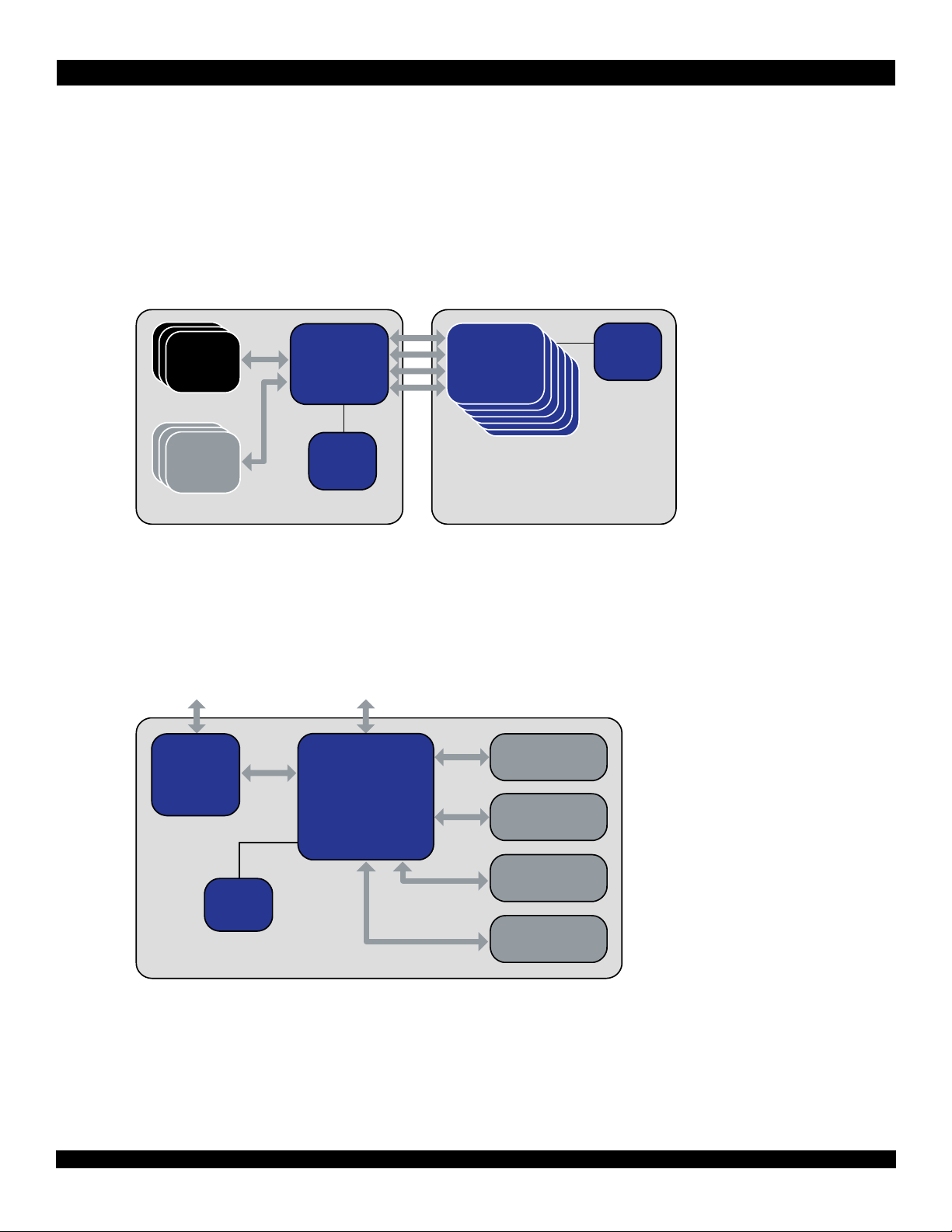
1. Device Overview > Typical Applications
4 x4 S-RIO
S-RIO Payload Card S-RIO x4 Switch Card
IDT Clock
156.25
MHz
CPS-1848
RapidIO
Switch
IDT Clock
156.25
MHz
FPGA
S-RIO
FPGA
S-RIO
FPGA
S-RIO
FPGA
S-RIO
FPGA
S-RIO
PowerPC
S-RIO
CPS-1848
RapidIO
Switch
CPS-1848
RapidIO
Switch
CPS-1848
RapidIO
Switch
CPS-1848
RapidIO
Switch
CPS-1848
RapidIO
Switch
CPS-1848
RapidIO
Switch
x4 S-RIO
x4 S-RIO
Backplane
CPS-1848
RapidIO Switch
IDT Clock
156.25
MHz
DSP S-RIO 2
DSP S-RIO 2
DSP S-RIO 2
DSP S-RIO 2
x4 S-RIO
x4 S-RIO
x4 S-RIO
x4 S-RIO
PCIe to
S-RIO
Bridge
1.4.2 Defense and Aerospace Application Benefits
• S-RIO Error Management Extension support including Time-to-Live enables fault-tolerant systems
• VITA 41, Open VPX, and ATCA fabric mappings enable rapid development of modular, standards-based systems
• RapidIO-standard true peer-to-peer networking allows scaling of arbitrary topology and simplifies hot swap software
implementation
• Per-port filter feature allows blocking errant packets or malicious attack (for example, denial of service, system memory
reads and writes)
Figure 4: Military Open VPX System Application
1.4.3 Video and Imaging Application Benefits
• 40 multicast masks per port provides strong support for broadcasting or multicasting a specific data stream to multiple
endpoints executing unique transforms, scaling, and CODECs
Figure 5: Video and Imaging Application
CPS-1848 User Manual 27 June 2, 2014
Formal Status This document is confidential and is subject to an NDA.
Integrated Device Technology
Page 28

2. RapidIO Ports
This chapter describes the S-RIO port functionality of the CPS-1848. Topics discussed include the following:
• Overview
• Key Features
• Packet Routing
• Flow Control
• Multicast Event Control Symbols
• Port Reconfiguration Operations
• Reset Control Symbol Processing
• Hot Extraction/Insertion
• Packet Trace and Filtering
• Packet Generation and Capture
• Packet Transfer Validation and Debug
2.1 Overview
Each CPS-1848 S-RIO port is compliant to the RapidIOSpecification (Rev.2.1). Each port provides the S-RIO defined
Physical Coding Sublayer (PCS) functionality and the packet exchange protocol management. Each port also connects to the
associated SerDes blocks and the switch fabric block, as displayed in Figure6.
CPS-1848 User Manual 28 June 2, 2014
Formal Status This document is confidential and is subject to an NDA.
Integrated Device Technology
Page 29
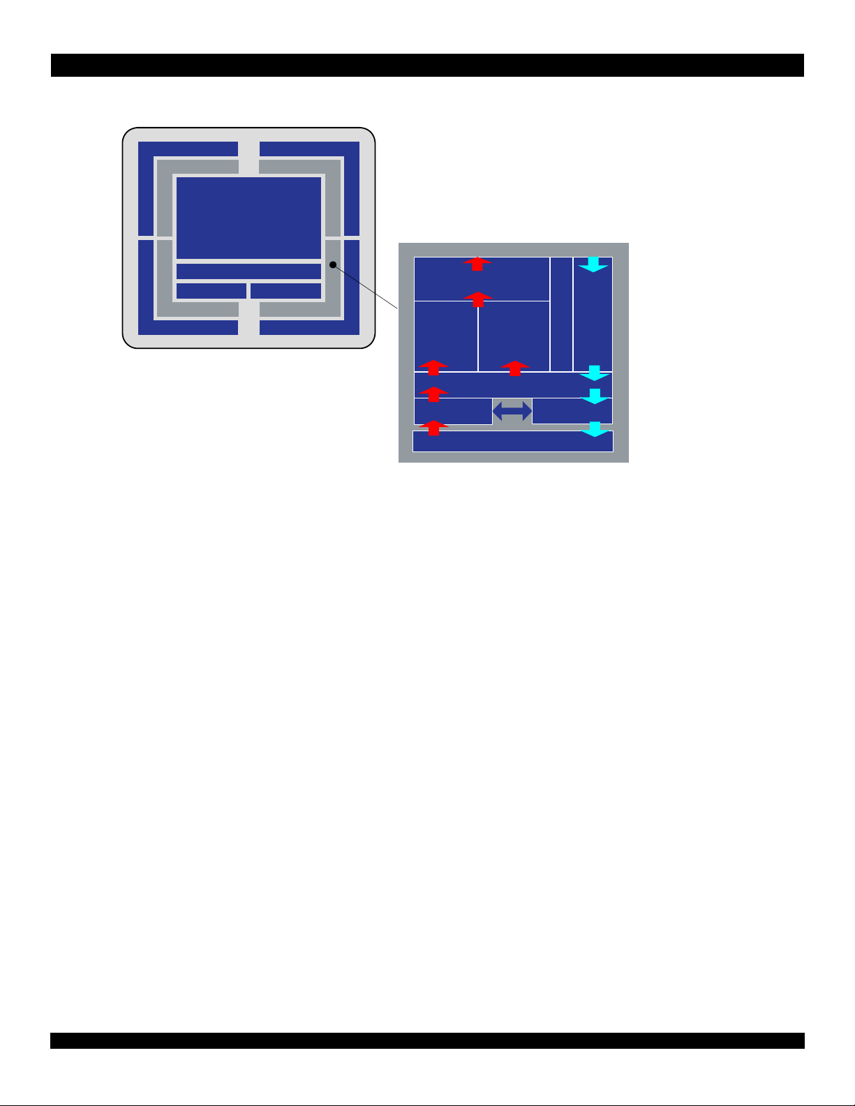
2. RapidIO Ports > Key Features
Lanes
Ports
Lanes
Ports
Lanes
Ports
Lanes
Switch
Fabric
Registers
I2C JTAG
Ports
Quadrant
Quadrant
Quadrant
Quadrant
Lane to Port Connection
Packet
Routing
Trace &
Filter
Input Buffer
CS RX CS TX
RapidIO Flow Control
Error Mgmt
Final Buffer
S-RIO Port Block
Figure 6: S-RIO Port Diagram
Figure 6 shows a block diagram of an S-RIO Port Block. The key components of this port diagram are discussed throughout
the chapter.
2.2 Key Features
The S-RIO Block supports the following:
• 8b/10b codec
• Data scrambling/descrambling
• Lane/Link initialization management
• Control symbol generation
• Control symbol reception/decode
• IDLE sequence generation/control
• Receiver- and transmitter-controlled flow control
• S-RIO-based reset support
• Packet retransmission management
• Link maintenance and software-assisted error recovery
• Packet transmission cancellation
• Link error detection and recovery
• Packet forwarding
• IDT-specifi c pac ke t trace and filtering
This functionality is compliant to the following S-RIO specifications:
• RapidIO Specification (Rev.2.1), Part 1: Input/Output Logical Specification
• RapidIO Specification (Rev. 2.1), Part 2: Message Passing Logical Specification
CPS-1848 User Manual 29 June 2, 2014
Formal Status This document is confidential and is subject to an NDA.
Integrated Device Technology
Page 30
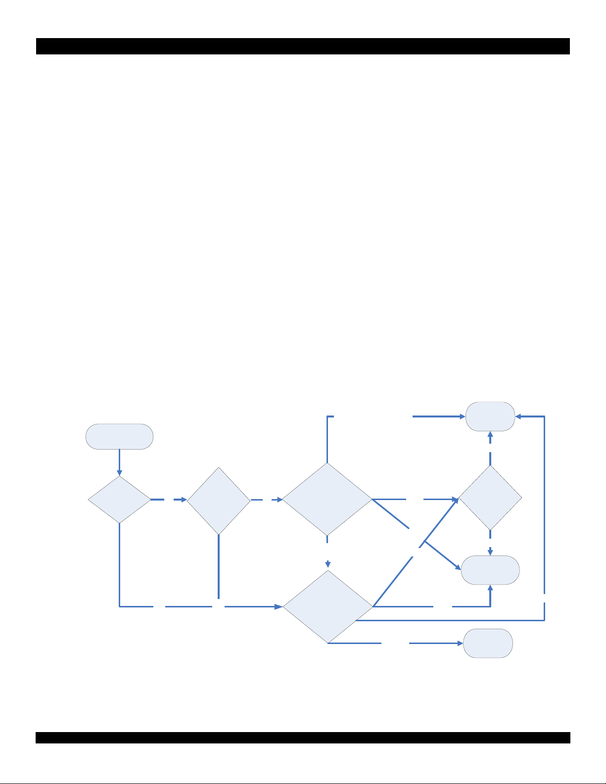
2. RapidIO Ports > Packet Routing
8-bit destID?
Yes
destID[15:8]
matches
RIO_DOMAIN
Use Device Route
(Value 0xDD)
Yes
destID In
DOMAIN ROUTE
Use destID[15:8] to
Index Domain Routing
Table
DEVICE ROUTE
Use destID[7:0] to
Index Local Routing
Table
Drop Packet
(0xDF)
RTE_
DEFAULT_
PORT_
CSR
Multicast
Mask
(0x40-0x67)
Send Packet
to Port n
Multicast, 0xDF or Invalid
Port n
0xDE
Port n
Multicast
0xDF
0xDF or Invalid
0xDE
P
o
r
t
n
No No
• RapidIO Specification (Rev.2.1), Part 3: Common Transport Specificat io n
• RapidIO Specification (Rev. 2.1), Part 6: LP-Serial Physical Layer Specification
• RapidIO Specification (Rev. 2.1), Part 7: System and Device Interoperability Specification
• RapidIO Specification (Rev.2.1), Part 8: Error Management Extensions Specification
• RapidIO Specification (Rev.2.1), Part 9: Flow Control Logic Layer Extensions Specification
• RapidIO Specification (Rev. 2.1), Part 11: Multicast Extensions Specification
• RapidIO Specification (Rev.2.1), Annex I: Software/System Bring Up Specification
2.3 Packet Routing
The main function of each S-RIO port is to route received packets to the appropriate port(s) on the switch. Packet routing is
supported in a RapidIO standard method usin g routing table s and standard RapidIO re gisters for mult icast functionality. Packet
routing is supplemented by implementation-specific registers for both the routing tables and for multicast. In addition, debug
features such as packet trace and filtering augment the normal packet routing.
The following sections describe routing table operation and programming, multicast operation and programming, and the
packet trace/filtering debug functionality.
2.3.1 Packet Routing Overview
Each S-RIO port provides a 256 entry Device Routing Table and a 256 entry Domain Routing Table. The scenario for the use
of the Domain and Device Routing Tables is a large system that has multiple chassis connected together, and multiple boards
in each chassis. The Domain Routing Table selects which chassis/board to route packets to, while the Device Routing Table
routes packets to a specific processing element on a board.
Figure 7: Routing Table Flowchart
CPS-1848 User Manual 30 June 2, 2014
Formal Status This document is confidential and is subject to an NDA.
Integrated Device Technology
Page 31

2. RapidIO Ports > Packet Routing
Figure 7 shows the decision tree for routing a received packet. The Device Routing Table routes packets with 8-bit destIDs,
and 16-bit destIDs whose most significant byte is 0. Packets with 16-bit destIDs whose most significant byte is non-zero are
routed using the Domain Routing Table, unless:
• The most significant 8 bits of the 16-bit destID match the value programmed in the RapidIO Domain Register, or
• The Domain Routing Table entry for the destID has a value of 0xDD.
Table 1 explains the meaning of the Domain and Device Routing Table port entry values, and restrictions on which values can
be programmed to the Domain or Device Routing Tables.
Programming a value into a routing table entry that is not allo wed accord ing to Table 1 causes packets
whose destID matches that routing table entry to be discarded.
Programming the number of a port that has no lanes assigned to it causes that packet to be dropped
(equivalent to No Route, value 0xDF).
Table 1: Route Table Reference Restrictions
Port Value Range Reference To
0x00–0x11 Port Numbers Yes Yes
0x12–0x3F Reserved No No
0x40–0x67
Multicast Mask Yes No
(0x40 + Mask Index)
0x68–0xDC Reserved No No
0xDD Force Local No Yes
0xDE Default Route Yes Yes
0xDF No Route Yes Yes
0xE0–FF Reserved No No
2.3.2 Unicast Programming Model
The CPS-1848 supports the RapidIO standard programming model through the following registers:
• Standard Route Table Entries Configuration destID Select CSR
• Standard Route Table Entry Configuration Port Select CSR
• Standard Route Table Entry Default Port CSR
Allowed in Device
Route Table
Allowed in Domain
Route Table
The Standard Route Table Entries Configuration destID Select CSR specifies the destID whose routing is affected by writ es to
the Standard Route Table Entry Configuration Port Select CSR. The Standard Route Table Entry Configuration Port Select
CSR can be read to determine the current route for a destID. Using the standard registers is called “indirect” routing table
programming.
Reading or writing a routing table e ntry requires two accesses. These accesses mu st be handled as an
atomic operation. If multiple software entities can access the routing table at the same time, mutual
exclusion must be enforced to ensure that one entity’s routing table updates do not corrupt another
entity’s efforts.
CPS-1848 User Manual 31 June 2, 2014
Formal Status This document is confidential and is subject to an NDA.
Integrated Device Technology
Page 32

2. RapidIO Ports > Packet Routing
Direct Routing Table Programming is the preferred access method in a multi-host system because it
does not require mutual exclusion.
The standard programming model requires one implementation-specific register, RapidIO Domain Register, to support the
Domain Routing Table. If the DESTID_MSB field of the Standard Route Table Entries Configuration destID Select CSR is 0, or
if the DESTID_MSB matches the destID located in the RapidIO Domain Register DOMAIN field, the Device Routing Table is
written. Otherwise, the LARGE_CFG_DEST_ID_MSB value determines which entry in the Domain Routing Table is updated.
As displayed in Unicast Programming Examples, ther e are some special values th at can be pr ogrammed into the routin g table.
If 0xDE is written, packets with that destID are routed according to the port specified in the Standard Route Table Entry Default
Port CSR. After reset, all destIDs are routed to the port value in this register:
• If 0xDD is programmed into the Broadcast Device Route Table Register {0..255}, the packet is discarded and the routing
table entry is overwritten with a value of 0xDF.
• If 0xDD is programmed into the Broadcast Domain Route Table Register {0..255}, packets that are in that domain are
routed according the Broadcast Device Routing Table.
• If a value of 0xDF is programmed into either the Domain or Device Routing Table, packets sent to that destID are
discarded.
The CPS-1848 supports routing table programming functions beyond what is indicated in the RapidIOSpecification (Rev. 2.1)
(see Programming Examples).
2.3.2.1 Per-Port Routing Tables
The CPS-1848 has a routing table for each port. This allows packets with the same destID to be routed differently depending
on which port they are received. This can be used to partition the switch, or to create virtual networks.
The Route Port Select Register selects whether all ports or one specific port is updated through the Standard Route Table
Entries Configuration destID Select CSR and Standard Route Table Entry Configuration Port Select CSR. The Route Port
Select Register default value selects all ports for routing table updates.
Port-writes generated by the CPS-1848 are routed using routing table entries that are programmed
using broadcast registers (for more information, see Port-Write Programming Model).
2.3.2.2 Extended Configuration Mode – Block Reads/Writes
The CPS-1848 supports the optional standard mechanism for reading or writing four routing table entries at once for the
Device Routing Table. These are called “Block” accesses. Block reads and writes are enabled by setting EXTD_EN to 1 i n the
Standard Route Table Entries Configuration destID Select CSR. A Block access can only occur when the DESTID_MSB
selects the Device Routing Table.
Block accesses cannot be performed to the Domain Routing Table. They can only be performed for
8-bit destIDs, or using 16-bit destIDs 0x0000 through 0x00FF.
When Block accesses are enabled, reading the Standard Route Table Entry Configuration Port Select CSR for a Device
Routing Table entry will return the values for four destIDs, starting with the destID specified in the Standard Route Table Entries
Configuration destID Select CSR.
If a Block Read exceeds the end of the Device Routing Table, the Block Read results are undefined.
For example, a Block Read for destID 0xFE will result in undefined data.
CPS-1848 User Manual 32 June 2, 2014
Formal Status This document is confidential and is subject to an NDA.
Integrated Device Technology
Page 33

2. RapidIO Ports > Packet Routing
When Block accesses are enabled, writing to the Standard Route Table Entry Configuration Port Select CSR for a Device
Routing Table entry will update the entry for the destID specified in the Standard Route Table Entries Configuration destID
Select CSR as well as the next three entries.
If a Block Write exceeds the end of the Device Routing Table, the Block Write wraps around to the
beginning of the routing table. For example, a Block Write for destID 0xFE will update routing table
entries for destIDs 0xFE, 0xFF, 0x00, and 0x01.
2.3.2.3 Direct Routing Table Programming
The CPS-1848 supports an implementation-specific routing table programming model whereby each routing table entry is
memory mapped into register space. Similar to the indirect model, registers are defined that affect the routing tables on every
port. Registers are also defined that affect just one port (see IDT Specific Routing Table Registers). Direct routing table
programming has the advantage of allowing multiple devices to read and write the routing tables with no mutual exclusion
requirements. Direct routing table programming also reduces the number of reads and writes that are required to configure a
routing table compared to the use of the standard registers. Depending on the specific programming needs, Block accesses
may be faster than direct routing table programming.
2.3.2.4 Maintenance Packet Routing
Maintenance packets are handled according to the hop count and destID fields. Maintenance packets with a non-zero hop
count are routed through the switch based on their destID. Maintenance packets can be multicast, however system behavior
when multicasting packets that require responses is not defined by the RapidIO Specification (Rev.2.1). Only port-write
packets should be multicast.
Maintenance packets with a zero hop count are processed by the switch. The response packet is sent out the port that
received the maintenance request. The source ID of the request packet becomes the destID of the response packet, and the
destID of the request packet becomes the sourceID of the response packet.
For Revision A/B, Maintenance packets are not ordered with respect to non-maintenance packets. For Revision C,
Maintenance packets with a non-zero hop count take the same path through the switch as non-maintenance packets.
2.3.3 Multicast Programming Model
The CPS-1848 supports the standard RapidIO programming model for multicast registers. This model consists of
programming the multicast masks that determine how a packet will be replicated, and then associating destIDs with multicast
masks. The registers include the following:
• Multicast Mask Port CSR – This register controls which destination ports are set in the multicast mask.
• Multicast Association Selection CSR – This register selects both the destID and multicast mask.
• Multicast Association Operations CSR – This register controls whether or not a destID is routed according to a multicast
mask.
The CPS-1848 handles 8-bit destIDs, and 16-bit destIDs that star t with 0x00 , as th e same. Formin g a n
association for an 8-bit destID 0xXX forms an association with the 16-bit destID 0x00XX. The TYPE bit
of the Multicast Association Operations CSR is ignored for 8-bit destIDs.
Multicast associations can be made only to destIDs in th e Devi ce Rout ing Table. The implication is that
only 8-bit destIDs, or 16-bit destIDs that are routed according to the Device Routing Table, can be
multicast.
The CPS-1848 supports multicast programming functions beyond what is specified in the RapidIOSpecification (Rev.2.1).
These functions are discussed in the following sections. For examples of multicast routing programming, see Multicast
Programming Examples.
CPS-1848 User Manual 33 June 2, 2014
Formal Status This document is confidential and is subject to an NDA.
Integrated Device Technology
Page 34

2. RapidIO Ports > Packet Routing
2.3.3.1 Per-Port Multicast Programming
Similar to the Unicast Programming Model, the CPS-1848 Multicast Programming Model allows each of the 40 multicast
masks, and the associations between destIDs and the multicast masks, to be unique for each port. This allows switches to be
partitioned, and to form virtual networks.
The Multicast Route Select Register controls which ports multicast masks are being controlled by the standard multicast
registers.
2.3.3.2 Direct Multicast Mask Programming
Also similar to the Unicast Programming Model, the CPS-1848 contains registers that memory map the multicast masks to
register space. There are registers defined that update a multicast mask for all ports (see Broadcast Multicast Mask Register
{0..39}), as well as port-specific multicast masks (see Port {0..17} Multicast Mask Register {0..39}).
Multicast routing requires a multicast mask to be associated with a destination ID. This can be accomplished by using the
device routing tables to associate a multicast mask with one or more destination IDs.
2.3.3.3 Broadcast Routing
The RapidIOSpecification (Rev. 2.1) requires that multicast packets are not replicated to the port that they are received on.
This allows one multicast mask to be shared among many endpoints that do not want to receive the data they have sent.
In some applications, it is useful to receive a message that has been multicast. This capability is supported by the CPS-1848
on a per-port basis through the use of the SELF_MCAST_EN bit in the Port {0..17} Operations Register.
2.3.4 Programming Examples
This section contains examples of successful routing table and multicast programming.
2.3.4.1 Unicast Programming Examples
Table 2: Unicast Programming Examples – Indirect Programming
Example Register Offset Value
Route destID 0x21 to port 3 for all ports. Standard Route Table Entries Configuration
0x70 0x00000021
destID Select CSR
Standard Route Table Entry Configuration Port
0x74 0x00000003
Select CSR
Route destID 0x43 to port 10 for port 7. Route Port Select Register 0x10070 0x00000008
Standard Route Table Entries Configuration
0x70 0x00000043
destID Select CSR)
Standard Route Table Entry Configuration Port
0x74 0x0000000A
Select CSR
Route destID 0x4321 to port 5 for all ports. Route Port Select Register 0x10070 0x00000000
Standard Route Table Entries Configuration
0x70 0x00004321
destID Select CSR
Standard Route Table Entry Configuration Port
0x74 0x00000005
Select CSR
CPS-1848 User Manual 34 June 2, 2014
Formal Status This document is confidential and is subject to an NDA.
Integrated Device Technology
Page 35

2. RapidIO Ports > Packet Routing
Table 2: Unicast Programming Examples – Indirect Programming (Continue d)
Example Register Offset Value
Route destID 0x5500–0x55FF according to the
RapidIO Domain Register 0xF20020 0x00000055
Device Routing Table for all ports.
Route destID 0x7700–0x79FF according to the
Device Routing Table for all ports.
Standard Route Table Entries Configuration
destID Select CSR
Standard Route Table Entry Configuration Port
0x70 0x00007700
0x74 0x000000DD
Select CSR
Standard Route Table Entries Configuration
0x70 0x00007800
destID Select CSR
Standard Route Table Entry Configuration Port
0x74 0x000000DD
Select CSR
Standard Route Table Entries Configuration
0x70 0x00007900
destID Select CSR
Standard Route Table Entry Configuration Port
0x74 0x000000DD
Select CSR
Set the default output port to 0x05. Standard Route Table Entry Default Port CSR 0x78 0x00000005
Route destID 0x7A00–0x7AFF to the default
port.
Standard Route Table Entries Configuration
destID Select CSR
Standard Route Table Entry Configuration Port
0x70 0x00007A00
0x74 0x000000DE
Select CSR
Discard all packets sent to destID 0x45. Standard Route Table Entries Configuration
0x70 0x00000045
destID Select CSR
Standard Route Table Entry Configuration Port
0x74 0x000000DF
Select CSR
Discard all packets sent to destID
0x7B00–0x7BFF.
Standard Route Table Entries Configuration
destID Select CSR
Standard Route Table Entry Configuration Port
0x70 0x00007B00
0x74 0x000000DF
Select CSR
Read Broadcast routing table entry for destID
0x88.
Standard Route Table Entries Configuration
destID Select CSR
Standard Route Table Entry Configuration Port
0x70 0x00000088
0x74 Read
Select CSR
Read Port 3 routing table entry for destID 0x99. Route Port Select Register 0x10070 0x00000004
Standard Route Table Entries Configuration
0x70 99
destID Select CSR
Standard Route Table Entry Configuration Port
0x74 Read
Select CSR
CPS-1848 User Manual 35 June 2, 2014
Formal Status This document is confidential and is subject to an NDA.
Integrated Device Technology
Page 36

2. RapidIO Ports > Packet Routing
Table 2: Unicast Programming Examples – Indirect Programming (Continue d)
Example Register Offset Value
Route destIDs 0x11, 0x12, 0x13 and 0x14 to
Route Port Select Register 0x10070 0x00000000
ports 10, 11, 12, and 13.
Standard Route Table Entries Configuration
0x70 0x80000011
destID Select CSR
Standard Route Table Entry Configuration Port
0x74 0x0D0C0B0A
Select CSR
Read the routing for destIDs 0x24, 0x25, 0x26,
and 0x27 for port 7.
Standard Route Table Entries Configuration
Route Port Select Register 0x10070 0x00000008
0x70 0x80000024
destID Select CSR
Standard Route Table Entry Configuration Port
0x74 Read
Select CSR
Table 3: Unicast Programming Examples – Direct Programming
Example Register Offset Value
Route destID 0x21 to port 3 for all ports. Broadcast Device Route Table Register {0..255} 0xE00084 0x00000003
Route destID 0x43 to port 10 for port 7. Port {0..17} Device Route Table Register
0xE1710C 0x0000000A
{0..255}
Route destID 0x43xx to port 5 for all ports. Broadcast Domain Route Table Register
0xE0050C 0x00000005
{0..255}
Route destID 0x5500 to 0x55FF according to
the Device Routing Table for all ports.
Route destID 0x7700 to 0x79FF according to
the Device Routing Table for all ports.
Broadcast Domain Route Table Register
{0..255}
Broadcast Domain Route Table Register
{0..255}
0xE00554 0x000000DD
0xE005DC 0x000000DD
0xE005E0 0x000000DD
0xE005E4 0x000000DD
Set the default port to 5. Standard Route Table Entry Default Port CSR 0x78 0x00000005
Route destID 0x7A00 to 0x7AFF to the default
port.
Broadcast Domain Route Table Register
{0..255}
0xE005E8 0x000000DE
Discard all packets sent to destID 0x45. Broadcast Device Route Table Register {0..255} 0xE00114 0x000000DF
Discard all packets sent to destID 0x7B00 to
0x7BFF.
Read Broadcast Routing Table entry for destID
Broadcast Domain Route Table Register
0xE005EC 0x000000DF
{0..255}
Broadcast Device Route Table Register {0..255} 0xE00220 Read
0x88.
Read Port 3 Routing Table entry for destID
0x99.
Port {0..17} Device Route Table Register
{0..255}
0xE13264 Read
CPS-1848 User Manual 36 June 2, 2014
Formal Status This document is confidential and is subject to an NDA.
Integrated Device Technology
Page 37

2. RapidIO Ports > Packet Routing
2.3.4.2 Multicast Programming Examples
Table 4: Multicast Programming Examples – Indirect Programming Model
Example Register Offset Value
Multicast DestID 0x01 to ports 4, 5, 6, and 7 on
all ports using multicast mask 0x27.
Reprogram Multicast Mask 0x20 to send to only
ports 10, 11, and 12.
Associate DestID 0x03 with Multicast Mask
0x20 on all ports except port 1 1. The association
is performed in two steps:
1. Associate all ports with the mask.
2. Disassociate port 11.
Multicast Mask Port CSR 0x80 0x00270410
0x00270510
0x00270610
0x00270710
Multicast Association Selection CSR 0x84 0x00010027
Multicast Association Operations CSR 0x88 0x00000060
Multicast Mask Port CSR 0x80 0x00200040
0x00200A10
0x00200B10
0x00200C10
Multicast Association Selection CSR 0x84 0x00030020
Multicast Association Operations CSR 0x88 0x00000060
Multicast Route Select Register 0x10080 0x0000000C
Multicast Association Operations CSR 0x88 0x00000020
1
Allow DestID 0xFF00 through FFFF to be
Route Port Select Register 0x10070 0x00000000
multicast according to the Device Routing Table
on all ports.
Standard Route Table Entries Configuration
destID Select CSR
Standard Route Table Entry Configuration Port
0x70 0x0000FF00
0x74 0x000000DD
Select CSR
1. When a multic ast mask is disassociated from a destID, the destID routing table value is 0xDF (drop packets).
CPS-1848 User Manual 37 June 2, 2014
Formal Status This document is confidential and is subject to an NDA.
Integrated Device Technology
Page 38

2. RapidIO Ports > Flow Control
Table 5: Multicast Programming Examples – Direct Programming Model
Example Register Offset Value
Multicast DestID 0x01 to ports 4, 5, 6 and 7 on
all ports using multicast mask 0x27.
Reprogram Multicast Mask 0x20 to send to only
ports 10, 11, and 12.
Multicast DestID 0x05 to ports 6, 7, 8 and 9
using multicast mask 3 on port 6 and mask 4 on
port 7, 8, and 9. Multicast will only occur for
packets received by ports 6, 7, 8 and 9.
Broadcast Multicast Mask Register {0..39} 0xF3009C 0x000000F0
Broadcast Device Route Table Register {0..255} 0xE00004 0x00000067
Broadcast Multicast Mask Register {0..39} 0xF30080 0x00001C00
Port {0..17} Multicast Mask Register {0..39} 0xF3860C 0x000003C0
Port {0..17} Device Route Table Register
0xE16014 0x00000043
{0..255}
Port {0..17} Multicast Mask Register {0..39} 0xF38710 0x000003C0
Port {0..17} Device Route Table Register
0xE17014 0x00000044
{0..255}
Port {0..17} Multicast Mask Register {0..39} 0xF38810 0x000003C0
Port {0..17} Device Route Table Register
0xE18014 0x00000044
{0..255}
Port {0..17} Multicast Mask Register {0..39} 0xF38910 0x000003C0
Port {0..17} Device Route Table Register
0xE19014 0x00000044
{0..255}
2.4 Flow Control
The CPS-1848 supports a variety of flow control functions. Receiver- an d transmitt er-controlled flow control are the most basic
RapidIO flow control functions. One of these fu nctions is always active on a link. In rece iver-controlled flow control, the r eceiver
tells the transmitter when it cannot accept a packet due to a lack of resources by issuing a retry. The transmitter then resumes
packet transfer with a packet of higher priority than the one that was retried, if such a packet is available, and retries (or
resends) the original packet at a later time, perhaps with increased priority.
Transmitter-controlled flow co ntro l is t he default mode of each port. In this mo de , t he transmitter only sends packets which the
receiver can accept. The choice between receiver- and transmitter-controlled flow control is made automatically as part of Port
and Lane Initialization Sequence. The flow co ntrol mode that is active on a link is reported in the RX_FC field of the Port {0..17}
Status and Control Register. For more information on receiver and transmitter-controlled flow control, see Part 6 of the
RapidIO Specification (Rev. 2.1).
2.4.1 Transmitter- and Receiver-Controlled Flow Control Programming Model
Transmitter- and receiver-controlled flow control decide which packets to send based on a packet’s priority. The CPS-1848
supports the four standard RapidIO priorities nu mbered 0 to 3 where 3 is the highest priority. The CPS-1848 also supports the
Critical Request Flow (CRF) bit which extends the number of priorities supported from four to eight.
Transmitter-controlled flow control can be disabled on a port using the TX_FLOW_CTL_DIS bit in the
Port {0..17} Operations Register.
CPS-1848 User Manual 38 June 2, 2014
Formal Status This document is confidential and is subject to an NDA.
Integrated Device Technology
Page 39

2. RapidIO Ports > Multicast Event Control Symbols
Priority 0, 1 and 2 packets all have buffer allocation values associated with them. These flow control values are called
“watermarks”, a shortened form of “high watermark”: the high est point on sho re that water reaches. Th e watermark associ ated
with a specific priority determines when a buffer is too full to accept/transmit packets of a specific priority. Note that there is no
watermark for priority 3 packets, since priority 3 packets must always be accepted whenever buffers are available.
When transmitter-controlled flow control is active on a port, the transmitter must have watermark values for the packets which
it transmits to the receiver. The watermarks reside in the Port {0..17} Watermarks Register. These watermarks define the
number of available buffers at which point packets of that priority will stop being transmitted. If a system is rarely congested,
the default values for this register will deliver optimal performance.
The watermark values in the Port {0..17} Watermarks Register should be set based on the buf fer size of
the link partner and the required traffic characteristics for packets of each priority. The default values
will result in optimal throughput when traffic is bursty and congestion is rare in the system, as they
maximize the number of low priority packets that can be accepted. When congestion is normal and
traffic of a specific priority must have guaranteed throughput, adjust the watermark values to reserve
sufficient buffers in the link partner. Depending on the link latency, two or three buffers per congested
priority must be reserved to ensure line rate throughput.
2.5 Multicast Event Control Symbols
Multicast Event Control Symbols (MECS) distribute events with l ow latency and littl e variability in di stribution dela ys throughout
a RapidIO system. An MECS can be received by a CPS-1848 port, or ca n be triggered b y the MCAST pin o n the device . Once
an MECS event has been received/triggered, the MECSs are transmitted by each port with the MCAST_CS field set to one in
the Port {0..17} Control 1 CSR. Note that the port which received the MECS does not transmit the MECS.
The CPS-1848 provides a physical pin called MCAST that can generate an MECS to all Multicast Event
participant egress ports (for more information, see the CPS-1848 Datasheet).
If two or more MECSs are received close enough in ti me tha t more th an one is waiti ng for transmi ssion
on a port, then at least one of them is forwarded. The o ther(s) ma y not be (Fo r information on minimum
period duration between MECSs, see Multicast-Event Control Symbol (MECS) Latency). The most
recently received MECS will be transmitted. Reg ardless of how many MECSs are received under these
conditions, at least one will be transmitted from each participant port.
2.6 Port Reconfiguration Operations
When one of the following port config uration events occur, a CPS-1848 port will require a re-initialization or reset (see Table 6).
Table 6: Port Reconfiguration Operations
Port Configuration Event Recommended Port Operation
Quadrant Configuration Register change Port reset (see PORT_SEL in Device Reset and Control
PLL {0..11} Control 1 Register.PLL_DIV_SEL change PLL reset (see PLL_SEL in Device Reset and Control
Lane {0..47} Control Register.TX_RATE or RX_RATE
Lane rate change
Register)
Register)
Port reset (see PORT_SEL in Device Reset and Control
Register). For examples of reconfiguring port and lane
speeds, see Lane and Port Speeds.
Port {0..17} Error and Status CSR.IDLE2_EN change Port reset (seePORT_SEL in Device Reset and Control
Register)
CPS-1848 User Manual 39 June 2, 2014
Formal Status This document is confidential and is subject to an NDA.
Integrated Device Technology
Page 40

2. RapidIO Ports > Reset Control Symbol Processing
Table 6: Port Reconfiguration Operations (Continued)
Port Configuration Event Recommended Port Operation
Lane {0..47} Control Register.LANE_DIS
Lane disable/enable
Port {0..17} Operations Register.TX_FLOW_CTL_DIS
TX Flow control disable/enable
These recommended port operations also apply when any of these port configuration events are
performed within an EEPROM load. After each event, the recommended operation should be
implemented within the EEPROM load (for more information, see the note in EEPROM Format).
2.6.1 Disabling IDLE2 Operation
When operating at lane speeds of 5 Gbaud or less, IDLE2 operation should be disabled in order to improve link performance,
as displayed in Table 7.
Table 7: Disabling IDLE2 Operation on Port 3
Step Register Offset Value
1. Disable IDLE2 by setting IDLE2_EN to 0. Port {0..17} Error
2. Perform a port reset by writing to PORT_SEL.
Port reset (see PORT_SEL in Device Reset and Control
Register)
Force-reinit required (see FORCE_REINIT in Port {0..17}
Operations Register)
0x0001B8 0x80000000
and Status CSR
1
Device Reset and
0xF20300 0x80000008
Control Register
3. Once the port achieves PORT_OK (PORT_OK is 1),
then disable IDLE2 on the connected port using
Port {0..17} Error
and Status CSR
maintenance packet, I2C, or JTAG.
1. After performing a port reset, clear Port {0..17} Error and Status CSR.PORT_ERR if it was set during the reset process
(for more information, see HS-LP Controlled Recovery). For Revision A/B devices, a Link-Request control symbol must
be sent to clear the fatal error condition before clearing PORT_ERR.
2.7 Reset Control Symbol Processing
A RapidIO device can be reset using a RapidIO reset request. This type of reset request consists of four reset request control
symbols received with no intervening control symbols, excep t status co ntro l symbols.
The CPS-1848 can handle a RapidIO reset request in one of two ways, ba sed on the value of the PORT_RST _CTL field of the
Device Control 1 Register. A value of 0 resets the entire CPS-1848, while a value of 1 resets just the port that received the
reset request. For more information about a “per-port” reset, see the following section.
2.7.1 Per-Port Reset
A per-port reset causes a RapidIO port to behave as follows:
1. All outstanding error states and retry states are cleared. This includes input-error and output-error.
2. All unacknowledged, transmitted packets are discarded, and tracking of transmitted packets is cleared.
3. Any current packet being received is discarded by the switch. The packet is not acknowledged.
4. Tracking of outstanding Link-Request/Input-Status (error recovery) control symbols is reset.
0x0001B8 -
CPS-1848 User Manual 40 June 2, 2014
Formal Status This document is confidential and is subject to an NDA.
Integrated Device Technology
Page 41

2. RapidIO Ports > Reset Control Symbol Processing
5. The next transmitted and received ackID values are reset to 0. The next packet to be transmitted by the port will have ackID
0. The expected ackID of the next packet is 0.
6. Detectable errors on control symbols or packets received by the port in the cycle in which the reset event occurs are ignored.
7. Packets stored in the port’s input buffer are discarded.
8. Packets stored in the crosspoint buffers that feed the port’ s final buffer of the port ar e discarded while the port is held in reset.
9. Packets stored in the port’s final buffer are discarded.
If many congested ports were sending packets to the reset port, some packets may exist in the final
buffer after the reset. It is also possible for maintenance responses to be sent after the reset because
maintenance requests with a hop count of 0 are processed outside of the receiving port.
10.The Port {0..17} Error and Status CSR is updated as follows:
— PORT_UNINIT is set to 1
— PORT_OK is set to 0
— INPUT_ERR_STOP is set to 0
— INPUT_ERR is set to 0
— INPUT_RETRY_STOP is set to 0
— OUTPUT_ERR_STOP is set to 0
— OUTPUT_ERR is set to 0
— OUTPUT_RETRY_STOP is set to 0
— OUTPUT_RETRIED is set to 0
— OUTPUT_RETRY is set to 0
— PORT_ERR is set to 0 (Revision C)
The following is applicable to Revision A/B.
PORT_ERR is not cleared by a per-port reset. If PORT_ERR is set then the port will drop all packets
routed to the Final Buffer, including maintenance packet responses.
To recover, the port must send a Link-Request/Input Status control symbol and receive a response.
This will clear the PORT_ERR and packet drop condition. The CPS-1848 will send a
Link-Request/Input Status control symbol when either of the following occurs:
• A Packet Not Accepted control symbol is received
• 0b100 is written to the Port {0..17} Link Maintenance Request CSR.CMD
For more information on clearing PORT_ERR, see HS-LP Controlled Recovery.
11.The link begins to retrain, starting from the SILENT state.
Routing table programming is retained after a per-port reset.
All registers other than the registers referenced above retain the values they had before the per-port
reset request was received.
Writing to the Port {0..17} Link Maintenance Request CSR for the co rrect port requires knowledge of the
port number on the link partner. If it is possible to be connected to one of many port s, i t is ne ce ssary to
write to the Port {0..17} Link Maintenance Request CSR for each port.
CPS-1848 User Manual 41 June 2, 2014
Formal Status This document is confidential and is subject to an NDA.
Integrated Device Technology
Page 42

2. RapidIO Ports > Hot Extraction/Insertion
2.7.2 Port Disable/Enable
When a port is disabled and then enabled by setting and clearing Port {0..17} Control 1 CSR.PORT_DIS, the behavior of the
port is as described in Per-Port Reset. The only differe nce i s th at packets a re discarde d for the entire period when PORT_DIS
is set.
ackID resynchronization is required when PORT_DIS is set and cleared.
The procedure for ackID resynchronization is specific to the link partner device. If the link partner is a
CPS Gen2 device, resetting the link partner port and the local port will resynchronize the ackIDs (for
more information, see System Controlled Recovery).
2.7.3 Generating a Reset Request
The CPS-1848 can generate a reset request to its link partner by writing 0x0000_0003 to the Port {0..17} Link Maintenance
Request CSR.
In some systems, it may be necessary to check that the link partner has acted on the reset request. This should be apparent
when the Port {0..17} Error and Status CSR PORT_OK bit is cleared, and the Port {0..17} Error and Status CSR
PORT_UNINIT bit is asserted. Event notification can be configure d to send a p ort- write o r asse rt an i nter rupt when this occurs
(for more information, see Event Management).
Once the link partner acts on the reset request, Port {0..17} Control 1 CSR.PORT_LOCKOUT should be asserted until the link
has retrained. This will cause all packets destined for the port to be discarded.
If the link partner accepts the reset, it will clear the expected and transmitted ackID values to 0. The Port {0..17} Local ackID
CSR should be cleared to 0, and the CLR bit in this register should be set to 1. This wi ll cause all outsta nding unackno wledged
packets to be dropped.
A Link-Request/Input-Status control symbol should be sent to the link partner by writing to Port {0..17}
Link Maintenance Request CSR[CMD] after a reset request followed by a link-response.
Alternatively, the procedure for hot insertion can reset the link partner and discard all packets, as described in Link Partner
Insertion.
2.8 Hot Extraction/Insertion
The hot extraction and insertion procedure is used to replace or upgrade hardware. It can also reset and then re-establish
communication with link partners, whether or not they have been physically replaced.
The following sections use the phrase “hot-swap link partner” (HS-LP) to identify the entity that is the
subject of the hot extraction/insertion or reset. The HS-LP can be the link partner of the CPS-1848, or
can be the CPS-1848 itself.
Hot Extraction/Insertion support requires exclusive use of t he followi ng registers. No Sta ndard Physi cal
Layer Errors can be enabled when Hot Extraction/Insertion functionality is required.
• Port {0..17} Error Report Enable Register
• Lane {0..47} Error Report Enable Register
• Port {0..17} Implementation Specific Error Rate Enable Register
CPS-1848 User Manual 42 June 2, 2014
Formal Status This document is confidential and is subject to an NDA.
Integrated Device Technology
Page 43

2. RapidIO Ports > Hot Extraction/Insertion
2.8.1 Hot Extraction
This section describes configuration options to manage controlled and uncontrolled removal/reset of the link partner. The
primary considerations when removing/resetting a link partner are:
• Timely notification that the link partner has been removed/reset
• Management of packets sent to the link partner when it has been removed/reset
• Isolation of the system from the link partner if the system design requires central coordination to admit new resources into
the system
• Preparing for link partner recovery
2.8.2 Controlled Removal/Reset
T o per form controlled removal or reset of a HS-L P, the following steps should be followed. Note that the programming mod el for
performing steps 1 to 4 is located in Preparation For Hot Extraction on Port Y.
1. Disable event notification for the HS-LP, except for extraction/insertion events.
2. Discard packets originated by or routed to the HS-LP.
3. Prevent acceptance of new packets from the HS-LP.
4. Reset and/or extract the HS-LP.
5. Confirm the reset/extraction by reception of an extraction event as described below.
6. Prepare the port for the insertion/return of the link partner as found in Preparation For Hot Insertion on Port Y.
Packets destined for a HS-LP usually should be discarded, since the link partner lacks the context and/or configuration to
correctly handle these packets. Also, if traf fic continues at a rate that can exhaust the swi tch buffers whi le the link partner is not
accepting packets, the system can congest and fail. For these reasons, it is assumed that the system should not have
transactions flowing in either direction through the CPS-1848 port when preparing for a hot extraction or link partner reset.
The act of removing/resetting the HS-LP will cause errors to be detected on the link. Additionally, since the link partner is no
longer present, events unrelated to hot swap/reset should be su ppre ssed. Events relat ed to ho t swap/re set can be re ceived to
confirm that the link partner has been removed and/or successfully reset.
Once link partner removal/reset has been confirmed, if the link partner is expected to reappear, the port must be prepared for
link partner insertion and/or reset completion.
CPS-1848 User Manual 43 June 2, 2014
Formal Status This document is confidential and is subject to an NDA.
Integrated Device Technology
Page 44

2. RapidIO Ports > Hot Extraction/Insertion
Table 8: Preparation For Hot Extraction on Port Y
Step Register Offset Mask and Value Description
1. Disable event
notification except for hot
swap events.
Port {0..17} Error
Rate CSR
Port {0..17} Error
Rate Threshold
CSR
Lane {0..47} Error
Rate Enable
Register
Port {0..17} Control
1 CSR
Port {0..17}
Operations
Register
0x1068 +
(0x40*Y)
0x106C +
(0x40*Y)
0xFF8010 +
(0x100 * lane_num)
0x00015C +
(0x20*Y)
F40004 +
(0x100*Y)
0x00000000 Disable error rate bias, clear error rate
counter.
0x01000000 Set error rate threshold to detect an
OUTPUT_FAIL condition (Port {0..17}
Error and Status CSR) if one or more
errors occur.
0x00000003 Enable error reporting for loss of lane
ready and loss of lane sync events.
Repeat for each lane associated with the
port.
0xXXXXXXXC Set STOP_ON_PORT_FAIL_ENC_EN
and DROP_PKT_EN bits to prevent
congestion when the link partner is
removed. For more information on when
STOP_ON_PORT_FAIL_ENC_EN and
DROP_PKT_EN are set, see Event
Isolation.
0x10000000
(PORT_INT_EN) or
0x08000000
Ensure at least one of PORT_INT_EN or
PORT_PW_EN is set to ensure notification
occurs.
(PORT_PW_EN)
2. Discard all packets sent
to the HS-LP.
3. Discard all packets
received from the HS-LP.
Port {0..17} Error
Report Enable
0x031044 +
(0x40*Y)
0x80000000 Enable port-writes and interrupt notification
for the Hot Extraction events.
Register
Port {0..17}
Implementation
Specific Error
Report Enable
Register
0x03104C +
(0x40*Y)
0x80000000 Disable all error reporting except
ERR_RATE_EN bit.
The default is all bits are enabled in the
register; however, this setup can trig ger an
unexpected event.
If port-writes are used, ensure that port-write destin ati ons an d ro uti ng are configured according to Port-Write
Formats, Programming Model, and Generation.
Configure routing tables to discard packets sent to this port, as describe d in Packet Routing. This should stop
packets from accumulating in the Final Buffer.
Configure the port’s routing table to discard al l packets receive d by this port, as described in Packet Routing.
This should stop requests from being issued by the HS-LP.
CPS-1848 User Manual 44 June 2, 2014
Formal Status This document is confidential and is subject to an NDA.
Integrated Device Technology
Page 45

2. RapidIO Ports > Hot Extraction/Insertion
Table 8: Preparation For Hot Extraction on Port Y (Continued)
Step Register Offset Mask and Value Description
4. Do not accept packets
from the HS-LP.
At this point, removing or resetting the link partner will result in an OUTPUT_FAIL and/or FATAL_ERR_PKT_MGT condition.
This will cause any packets in the final buffer of the CPS-1848 port connected to the HS-LP to be discarded.
T o g uarantee that all packets asso ciated with the HS-LP have been discarded, it is necessary to wa it for
the Time-to-Live (TTL) timeout period before allowing the HS-LP back in to the system. The TTL value
is programmed using Packet Time to Live CSR.TTL.
Packets associated with the HS-LP may have been discarded by the actions taken above. For
deterministic operation, IDT recommends that the HS-LP is reset.
A port-write or interrupt indicating an OUTPUT_FAIL or PORT_ERR standard event acts as confirmation that the HS-LP has
been removed or reset. Once this confirmation is received, the system can prepare the CPS-1848 port to bring the HS-LP back
into the system.
Port {0..17} Control
1 CSR
Device Control 1
Register
0x15C + (0x20*Y) 0xXXXXXXXF Ensure PORT_LOCKOUT,
STOP_ON_PORT_FAIL_ENC_EN, and
DROP_PKT_EN are set.
Note: Responses may be in flight to/from
the HS-LP at this point.
0xF2000C 0x0XXXXXXX Ensure that the FATAL_ERR_PKT_MGT
bit is cleared. Packets sent to the HS-LP
will be discarded due to the port error
detected.
Port preparation consists of the following:
1. Clearing all error conditions on the port
2. Continuing to isolate the HS-LP from the remainder of the system
3. Receiving notification when the HS-LP has reappeared
Isolation of the HS-LP and notification of HS-LP reappearance are only necessary when it is the responsibility of system
software, not the HS-LP, to bring the HS-LP back into the system.
Table 9: Preparation For Hot Insertion on Port Y
Step Register Offset Value Description
1. Clear all error
conditions on Port Y.
Device Reset and
Control Register
Ensure Port {0..17} Implementation Specific Error Detect Register.PORT_INIT bit is not set due to the hot
extraction. If it is set, write a 0 to clear it.
0xF20300 0x8000YYYY Perform a per-port reset on port Y to clear
errors. Note that “YYYY” in the Value
column is a vector with bit “Y” set.
CPS-1848 User Manual 45 June 2, 2014
Formal Status This document is confidential and is subject to an NDA.
Integrated Device Technology
Page 46

2. RapidIO Ports > Hot Extraction/Insertion
Table 9: Preparation For Hot Insertion on Port Y (Continued)
Step Register Offset Value Description
2. Isolate the HS-LP from
the remainder of the
system.
3. Configure event
management for
notification.
Configure the port’s routing table to discard al l packets receive d by this port, as described in Packet Routing.
This should stop requests from being issued by the HS-LP.
Configure the device's routing table to discard all packets sent to this port, as described in Packet Routing.
This should stop requests from being issued to the HS-LP.
Port {0..17} Control
1 CSR
0x15C +
(0x20*Y)
0xXXXXXXXF Ensure PORT_LOCKOUT,
STOP_ON_PORT_FAIL_ENC_EN and
DROP_PKT_EN are set. Note: There may
be responses in flight to and from the
HS-LP at this point. For more information
on when
STOP_ON_PORT_FAIL_ENC_EN
and DROP_PKT_EN are set, see Event
Isolation.
Port {0..17} Error
Report Enable
0x31044 +
(0x40*Y)
0x80000000 Enable reporting for
implementation-specific errors.
Register
Port {0..17}
Implementation
Specific Error
Report Enable
Register
0x3104C +
(0x40*Y)
0x00000020 Ensure that the PORT_INIT_EN event is
enabled. This indicates when the port has
successfully trained.
Note: No other error events will be
reported by the port until the port has
initialized.
Port {0..17}
Operations
Register
If port-writes are used, ensure that port-write destin ati ons an d ro uti ng are configured according to Port-Write
Formats, Programming Model, and Generation.
2.8.2.1 Unexpec ted Extraction
In systems that do not have central control software, or those that allow the removal of components without prior coordination
with the system, it is by definition not possible to perform the steps in Controlled Removal/Reset. It is only possible to recover
the system after a component is removed.
This recovery process consists of the following considerations:
1. All packets destined for the removed component must be discarded automatically.
2. The remaining components of the system may need to be informed that the component has been removed.
3. The link may need to be prepared for the HS-LP to bring itself back into the system.
Automatic discard of packets destined for a failed port uses a method similar to that described in Controlled Removal/Reset.
An unexpected extraction cannot be distinguished from link re-initialization. This implies that if a link
re-initializes, the system will react as if the link partner has been removed and re-inserted.
F40004 +
(0x100*Y)
0x10000000
(PORT_INT_EN) or
0x08000000
(PORT_PW_EN)
Ensure at least one of PORT_INT_EN or
PORT_PW_EN is set to ensure notification
occurs.
CPS-1848 User Manual 46 June 2, 2014
Formal Status This document is confidential and is subject to an NDA.
Integrated Device Technology
Page 47

2. RapidIO Ports > Hot Extraction/Insertion
Informing the remaining components in the system of th e HS- LP's extracti on ca n b e compl ete d b y mu lti casting a port-write, or
through a shared interrupt.
Table 10: Preparation of Port That Can be Subjected to Unexpected Hot Extraction Event
Step Register Offset Value Description
1. Enable event
notification.
Port {0..17} Error
Rate CSR
Port {0..17} Error
Rate Threshold
CSR
Lane {0..47} Error
Rate Enable
Register
Port {0..17} Control
1 CSR
Port {0..17}
Operations
Register
Port {0..17} Error
Report Enable
Register
0x1068 +
(0x40*Y)
0x106C +
(0x40*Y)
0xFF8010 +
(0x100 * lane_num)
0x00015C +
(0x20*Y)
F40004 +
(0x100*Y)
0x031044 +
(0x40*Y)
0x00000000 Disable error rate bias, clear error rate
counter.
0x01000000 Set error rate threshold to detect an
OUTPUT_FAIL condition (Port {0..17}
Error and Status CSR) if one or more
errors occur.
0x00000003 Enable error reporting for loss of lane
ready and loss of lane sync events.
Repeat for each lane associated with the
port.
0xXXXXXXXC Set STOP_ON_PORT_FAIL_ENC_EN
and DROP_PKT_EN bits to prevent
congestion when the link partner is
removed.
0x10000000
(PORT_INT_EN) or
0x08000000
Ensure at least one of PORT_INT_EN or
PORT_PW_EN is set to ensure notification
occurs.
(PORT_PW_EN)
0x80000000 Enable port-writes and interrupt notification
for the Hot Extraction events.
Port {0..17}
Implementation
Specific Error
Report Enable
Register
0x03104C +
(0x40*Y)
0x80000000 Disable all error reporting except
ERR_RATE_EN bit.
The default is all bits are enabled in the
register; however, this setup can trig ger an
unexpected event.
If port-writes are used, ensure that port-write destin ati ons an d ro uti ng are configured according to Port-Write
Formats, Programming Model, and Generation.
After a surprise extraction, if system software is responsible for bringing a new link partner into the syste m, the steps described
in Table 8 and Table 9 should be performed to ensure that all packets in flight to/from the HS-LP are discarded, and that
system software is informed when the HS-LP reappears in the system.
CPS-1848 User Manual 47 June 2, 2014
Formal Status This document is confidential and is subject to an NDA.
Integrated Device Technology
Page 48

2. RapidIO Ports > Hot Extraction/Insertion
2.8.3 Link Partner Insertion
Similar to extraction, the steps required to deal with insertion of a link partner depend on whether system software is
responsible for allowing the HS-LP into the system, or if the HS-LP is responsible for bringi ng itself into t he system. In general,
the entity responsible for bringing the HS-LP into the system is called the Recovery Controller.
Once the HS-LP has been inserted, the ability to transfer maintenance packets must be re-established as a first step toward
the HS-LP’s participation in the system. The extraction of an HS-LP usually causes multiple errors to be detected. By design,
these errors include link communication failure and can include packet discard. These errors can prevent the transfer of
maintenance packets. To establish maintenance packet transfer, it is necessary to achieve the fol lowi ng two obje ct ives:
1. Clear error conditions on the link, which may have occurred during hot insertion
2. Ensure ackID synchronization between the HS-LP and the link partner
The procedure for clearing error conditions and synchronizing ackIDs depends on whether the HS-LP or another node in the
system is the Recovery Controller, and the specific link configuration. Common scenarios involving the CPS-1848 are
described in the following sections. Application notes for hot extraction/hot insertion of other devices are also available from
www.idt.com.
Once maintenance packets can be exchanged, the Recovery Controller can then do the following:
1. Undo whatever preparation was done due to a controlled extraction
2. Clear any other error conditions associated with an uncontrolled extraction
3. Bring the HS-LP back into the system
These steps are system specific, and so are not described here.
2.8.3.1 System Cont rolled Recovery
The procedure described in Table 11 assumes that the steps captured in Table 8 and Table 9 were performed, whether the
extraction was controlled or uncontrolled.
The steps in Table 9 should be performed for all ports that do not have link partners wh en the syste m is
powered up, but which could have link partners inserted on them while the system is operating.
When the Recovery Controller resides on the CPS-1848 side of the link connected to the HS-LP, it is
assumed that the HS-LP has been reset. To guarantee that this is the case, IDT recommends that the
Recovery Controller reset the HS-LP as part of this procedure. This ensures consistent starting
conditions if the link initialization was not the result of a hot-swap event.
CPS-1848 User Manual 48 June 2, 2014
Formal Status This document is confidential and is subject to an NDA.
Integrated Device Technology
Page 49

2. RapidIO Ports > Hot Extraction/Insertion
Table 11: System Recovery Controller Operation, HS-LP on Port Y
Step Register Offset Value Description
1. Establish routing
to/from the HS-LP.
2. Disable event
notification and isolation
functions.
Configure routing tables to allow maintenance access to CPS-1848 port an d the HS-L P. The procedures are
described in Packet Routing.
Port {0..17} Error
0x1044 + (0x40*Y) 0x00000000 Disable all events
Rate Enable CSR
Port {0..17} Error
0x106C + (0x40*Y) 0x00000 00 0 Disable OUTPUT_FAIL condition on
Rate Threshold
CSR
Lane {0..47} Error
Rate Enable
0xFF8010 +
(0x100 * lane_num)
Register
3. Reset the HS-LP and
CPS-1848 port Y
Port {0..17} Control
1 CSR
Port {0..17} Local
ackID CSR
0x15C +
(0x20*port_num)
0x140 + (0x20*Y) 0x80000000 Clear outstanding packets, and clear
simultaneously.
Port {0..17} Link
0x140 + (0x20*Y) 0x00000003 Issue a “reset” request to the HS-LP. This
Maintenance
Request CSR
implementation specific event (see Port
{0..17} Error and Status CSR).
0x00000000 Disable error reporting.
Repeat for each lane associated with the
port.
Value is p ort
specific
Ensure PORT_LOCKOUT,
STOP_ON_PORT_FAIL_ENC_EN, and
DROP_ENABLE are cleared.
ackIDs to 0.
register can be written more than once to
ensure that the link partner receives a valid
reset request.
Port {0..17} Link
Maintenance
Response CSR
Device Reset and
Control Register
Port {0..17} Link
Maintenance
Request CSR
0x144 + (0x20*Y) Read Confirm that the reset request has been
sent.
0xF20300 0x8000YYYY Perform a per-port reset on port Y to clear
errors.
Note: This step should be performed
immediately after resetting the HS-LP to
clear error conditions at both ends of the
link simultaneously.
0x140 + (0x20*Y) 0x00000004 Issue a Link Request/Input Status request
to the HS-LP. This will clear a PORT_ERR
failure on the CPS-1848 port, if it exists,
and allow packets to be sent.
CPS-1848 User Manual 49 June 2, 2014
Formal Status This document is confidential and is subject to an NDA.
Integrated Device Technology
Page 50

2. RapidIO Ports > Hot Extraction/Insertion
2.8.3.2 HS-LP Controlled Recovery
If the HS-LP is the Recovery Controller then recovery of the link requires the procedure in Table 12 to be completed. Note that
the procedure assumes that the HS-LP is another CPS-18 48, or a device wi th a co mp ati bl e pro gra mmin g mod el. If th e HS-LP
is not a CPS-1848 then HS-LP implementation-specific register accesses may be necessary. Register references made with
address computations are for the CPS-1848. Register references made without address computations are for the HS-LP.
The procedure in Table 12 assumes that both the HS-LP and the CPS-1848 are connected using a cable. This implies that
each end of the new link could have exchanged packets with different link partners prior to connecting the cable.
The HS-LP port must support the Software Assisted Error Recovery version of the LP-Serial Extended Feature Block to
successfully resume packet exchange on the link.
Ta ble 12: HS-LP Recov ery Control ler
Step Register Offset Value Description
1. Clear ackIDs and
reinitialize HS-LP (Local)
port.
2. Disable and clear error
conditions that prevent
transmission of link
requests by the HS-LP
(Local).
3. Reset HS-LP (Local)
and CPS-1848 (Remote)
to clear link errors.
Device Reset and
Control Register
or
Implementation
Specific
Port {0..17} Error
Rate Enable CSR
Port {0..17} Error
Rate Threshold
CSR
Port {0..17} Error
Rate CSR
Lane {0..47} Error
Rate Enable
Register
Port {0..17} Error
and Status CSR
Port {0..17} Link
Maintenance
Request CSR
0xF20300
HS-LP (Local)
0x1044 + (0x40*Y)
HS-LP (Local)
0x106C + (0x40*Y)
HS-LP (Local)
0x1068 + (0x40*Y)
HS-LP (Local)
0xFF8010 +
(0x100 * lane_num)
HS-LP (Local)
0x000158 +
(0x20*Y)
HS-LP (Local)
0x000140 +
(0x20*Y)
HS-LP (Local)
0x8000YYYY
or
Implementation
Specific
Reset HS-LP (Local) port n.
If the HS-LP (Local) is not a CPS-1848
(Remote), the register address and value
written are implementation specific.
0x00000000 Disable all events.
0x00000000 Disable OUTPUT_FAIL condition on
implementation specific event (see Port
{0..17} Error and Status CSR).
0x00000000 Clear ERR_RATE_CNTR value.
0x00000000 Disable error reporting. Repeat for each
lane associated with the port.
0x07000000 Clear OUTPUT_DROP, OUTPUT_FAIL,
and OUTPUT_DEGR.
0x00000003 Issue a “reset” request to the CPS-1848.
Note: The CPS-1848 must have Device
Control 1 Register.PORT_RST_CTL set to
1 to perform per-port resets.
Device Reset and
Control Register
or
Implementation
Specific
0xF20300
HS-LP (Local)
0x8000YYYY
or
Implementation
Specific
Reset HS-LP (Local) port n. Register
values are given assuming that the HS-LP
(Local) is a CPS-1848 (Remote). If the
HS-LP (Local) is not a CPS-1848
(Remote), the register address and value
written are implementation specific.
Note: This step should be performed
immediately after resetting the CPS-1848
(Remote) to clear error conditions at both
ends of the link simultaneously.
CPS-1848 User Manual 50 June 2, 2014
Formal Status This document is confidential and is subject to an NDA.
Integrated Device Technology
Page 51

2. RapidIO Ports > Hot Extraction/Insertion
Ta ble 12: HS-LP Recov ery Control ler (Continued)
Step Register Offset Value Description
4. HS-LP (Local) clears
potential input-error
stopped state on the
CPS-1848 (Remote).
5. Check for error
conditions.
6. If the CPS-1848
(Remote) port is known,
clear ackIDs.
If the CPS-1848 (Remote)
port is not known, skip
step 6 and proceed to
step 7.
Port {0..17} Link
Maintenance
Request CSR
Device Identity
CAR
Port {0..17} Local
ackID CSR
Device Reset and
Control Register
or
Implementation
Specific
0x000140 +
(0x20 * Y)
HS-LP (Local)
0x000000
CPS-1848
(Remote)
0x000148 +
(0x20 * Y)
CPS-1848
(Remote)
0xF20300
HS-LP (Local)
0x00000004 After reset, the CPS-1848 (Remote) may
be in the input-error stopped state. Issue
an “input-status” request to the CPS-1848
(Remote).
Read Read the Device Identity CAR of the
CPS-1848. If the read completes
successfully then packet exchange can
resume.
Note: If the CPS-1848 always experiences
a PORT_ERR condition on extraction, do
not perform this step.
0x80000000 Clear ackIDs on the CPS-1848 (Remote)
port.
0x8000YYYY
or
Implementation
Specific
Reset HS-LP (Local) port n. Register
values are given assuming that the HS-LP
(Local) is a CPS-1848 (Remote). If the
HS-LP (Local) is not a CPS-1848
(Remote), the register address and value
written are implementation specific.
Port {0..17} Link
Maintenance
Request CSR
0x000140 +
(0x20 * Y)
HS-LP (Local)
0x00000003 Issue a “reset” request to the CPS-1848
(Remote).
Note: The CPS-1848 (Remote) must have
Device Control 1
Register.PORT_RST_CTL set to 1 to
perform per-port resets.
Packet exchange can resume once the link has completed initialization. Clear error status bits on HS-LP
(Local) and CPS-1848 (Remote).
CPS-1848 User Manual 51 June 2, 2014
Formal Status This document is confidential and is subject to an NDA.
Integrated Device Technology
Page 52

2. RapidIO Ports > Hot Extraction/Insertion
Ta ble 12: HS-LP Recov ery Control ler (Continued)
Step Register Offset Value Description
7. If the CPS-1848
(Remote) port is not
known, resynchronize
ackIDs.
For each CPS-1848 (Remote) port that the HS-LP (Local) can be connected to {
For ackID from 0 up to N (where N is 31 for IDLE1 and 63 for IDLE2) {
Write ackID to HS-LP (Local) Port {0..17} Local ackID CSR.INBOUND while retaining outstanding/outbound
values.
Write 0x4 to CPS-1848 (Remote) Port {0..17} Link Maintenance Request CSR.CMD
Read HS-LP (Local) Port {0..17} Local ackID CSR.INBOUND
If INBOUND <> ackID
Exit both loops, ackID resynchronization complete.
}
}
Port {0..17} Local
ackID CSR
Port {0..17} Local
ackID CSR
0x00148 +
(0x20*Y)
HS-LP (Local)
0x00148 +
(0x20*Y)
CPS-1848
0x0000YYYY Clear HS-LP (Local) inbound ackID while
retaining existing outstanding/outbound
ackID.
0x81000000 Clear outstanding/outbound ackID on
CPS-1848 (Remote) and set inbound
ackID to 0x01.
(Remote)
Port {0..17} Local
ackID CSR
0x00148 +
(0x20*Y)
0x80000000 Clear own ackID.
HS-LP (Local)
Port {0..17} Link
Maintenance
Request CSR
Device Reset and
Control Register
or
Implementation
Specific
0x00140 +
(0x20*Y)
HS-LP (Local)
0xF20300
HS-LP (Local)
0x00000003 Issue a “reset” request to the CPS-1848
(Remote).
0x8000YYYY or
Implementation
Specific
Reset HS-LP (Local) port n. Register
values are given assuming that the HS-LP
(Local) is a CPS-1848 (Remote). If the
HS-LP (Local) is not a CPS-1848
(Remote), the register address and value
written are implementation specific.
Clear error status bits on HS-LP (Local) and CPS-1848 (Remote). Packet exchange can now resume.
CPS-1848 User Manual 52 June 2, 2014
Formal Status This document is confidential and is subject to an NDA.
Integrated Device Technology
Page 53

2. RapidIO Ports > Packet Trace and Filtering
Packet Data
bit
0
..............................................bit
n<160
bit
0
........................................................................................bit
160
Comparison Data
Comparison Mask
bit
0
..............................................bit
n<160
X
n+1
................................X
160
X = don’t care
2.9 Packet Trace and Filtering
2.9.1 Packet Trace
Each S-RIO port can compare a received packet against a set of configurable predefined values, and, if a match occurs,
include a reference to a configurable output port as part of its forwarding information passed to the switch fabric. This function
is defined as the “Trace” function. When all bits of the packet data match corresponding bits in a spe cific prog rammabl e value
(after the value’s mask has been applied), the Trace Criteria is met and a copy of the packet is forwarded to the trace enabled
output port.
Each S-RIO port provides output port routing references derived from a received packet's destID (including multicast
references), as well as a routing reference to the configured trace port to the switch fabric. Each S-RIO port also provides a
uniquely configurable trace function so that trace can be enabled on up to 18 ports simultaneously. To enable the trace
function, set TRACE_EN to 1 in the Device Control 1 Register.
2.9.1.1 Trace Criteria
The property of an S-RIO port matching a packet with a “Trace Criteria” refers to a successful comparison of the first 160 bits
in a received packet to multiple pre-programmed values stored at that port. A successful match against a Trace Criteria will
trigger the S-RIO port to flag the trace port (to the switch fabric) for packet forwarding.
Each S-RIO port provides a set of four uniquely configur able 160-bit compari son values tha t can selectivel y be appl ied usi ng a
bit mask to the first 160 bits of each packet that the block receives. Each S-RIO port also provides a bit mask for each of the
four programmable 160-bit comparison values that define which of the first 160 bits of packet data are relevant to the
comparison. A value of 1 in the comparison value mask indicates that the corre sponding bits in the pro grammed va lue and th e
corresponding bit in the packet data is co mp ared . A val ue of 0 in the comparison value mask is used as a “don’t ca re”. A don’t
care value will result in an automatic match of the corresponding bits in the pro grammable value with the correspond ing packet
data bits. When all bits of the packet data match with a corresponding bit in a specific programmable value (after the value’s
mask has been applied) the Trace Criteria has been met and a copy of the packet is forwarded to the trace enabled output
port. The packet trace is triggered by a logical “OR” of the comparison match results (packet data with the four programmable
values) such that if at least one match occurs, packet forwarding to the trace enabled port is enabled.
Note that the trace criteria is based on the entire contents of the comparison value and its corresponding bit mask. If the
number of bits in the packet being compared is less than 160 bits, the excess bits in the mask must be set as “don't care,” as
displayed in Figure8.
Figure 8: Trace Criteria
The Trace Criteria architecture is displayed in Figure9.
CPS-1848 User Manual 53 June 2, 2014
Formal Status This document is confidential and is subject to an NDA.
Integrated Device Technology
Page 54

2. RapidIO Ports > Packet Trace and Filtering
0159
First 160 bits of packet
0 159
Programmable Comparison 0
Mask 0
Mask 1
Programmable Comparison 1
Mask 2
Mask 3
Programmable Comparison 2
Programmable Comparison 3
Trigger
0159
0 159
0 159
0 159
0 159
0 159
0 159
RapidIO
packet
Figure 9: Trace Function within a Port
From an application perspective, the support for comparison over the first 160 bits of the packet is to ensure that the trace
function can cover the largest RapidIO header (including those using extended add ressi ng ) plus at le ast the first 32 bits of the
payload. This implementation is flexible across the first 160 bits of the packet and ensures that the following parameters
(among others) can be used as trace criteria:
• The header’s ftype field (4 bits)
• The header’s destID field (8 or 16 bits)
• The header’s mbox field (up to 8 bits)
• The first 32 bits of the packet payload (32 bits)
If an S-RIO port detects an error in a received packet, the packet will not be forwarded to the trace port;
however, it can still be reported as a trace match.
2.9.1.2 Trace Port Features
Each S-RIO port supports a trace port functionali ty. The user can define which output port is enabled for the T race function. For
a specific device, all packets that match the Trace criteria from all trace-enabled inputs are routed to the same configured,
trace-enabled output port.
Note that the device supports configurations where the trace port and the output port referenced by a received packet are
defined to be the same port. In the case where there is a trace match and the packet’s destID references the output port
configured as the trace port, the packet will be forwarded only once regardless of the packet type.
CPS-1848 User Manual 54 June 2, 2014
Formal Status This document is confidential and is subject to an NDA.
Integrated Device Technology
Page 55

2. RapidIO Ports > Packet Trace and Filtering
2.9.1.3 Trace Routing Features
Each S-RIO port supports two operation modes for the trace routing function:
• Default Trace Routing – Device Control 1 Register.TRACE_OUTPUT_PORT_MODE = 0
• Optional Trace Routing – Device Control 1 Register.TRACE_OUTPUT_PORT_MODE = 1
2.9.1.3.1 Default Trace Routing Mode
In default mode, the trace enabled S-RIO p ort accepts RapidIO t raf fic (referenced by the received packet’s d estID field) as well
as traffic that matches the trace criteria of all po rts. T race-tri ggered packets are h andled by the tra ce-enabled output port in the
same way as it handles all other packets. Normal RapidIO priority and flow control rules apply.
2.9.1.3.2 Optional Trace Routing Mode
In optional mode, only packets that have matched a port’s trace criteria are routed to the trace port. A received packet that
does not match the Trace Cr iter ia, but whose destID field references the trace enabled output port wi ll no t be forwa rde d to the
trace port. If this packet has a destID that references a multicast operation that incl udes th e trace port, th e packet is forwarded
to all ports except for the trace enabled port. A packet that does not match a port’ s trace criteria who se destID only ref erenc es
the trace port is handled as an error packet and is dropped. Trace-triggered packets are handled by the trace-enabled output
port in the same way as it handles all other packets. Normal RapidIO priority and flow control rules apply.
A user can configure the trace port into “trace only” mode, and at the same time configure the port’s route table to allow
packets to be routed to the trace port (including packets that do not match the trace criteria). With this configuration, packets
received by a port that are to be routed to the trace port (as defined by that port’s route table) will be dropped by the device if
they do not match the trace criteria. Packets in this scenario that match the trace criteria are forwarded.
2.9.1.3.3 Maintenance Packets with Enabled Trace Ports
Type 8 packe ts are handled in the same way as all other packets for both Trace Routing Modes defined above. Type 8 packets
that are received at a trace-enabled input port that have a hop count of 0 are forwarded to the trace port if the trace criteria at
that port is met.
For Revision C, a Maintenance packet with a hop count greater than 0 is forwarded to the destination
port(s) with its hop count decremented by 1. The same packet (with its hop count de cremente d by 1) is
also forwarded to a trace port if trace criteria is matched.
For Revision A/B, a Maintenance packet with a hop count greater than 0 is forwarded to a trace port if
trace criteria is matched, however, its hop count remains unchanged. The same packet (with its hop
count now decremented by 1) is forwarded to the destination port(s).
2.9.1.3.4 No Route Conditions
Packets that meet the trace criteria are routed to the trace port even if the packet destID reference in the port’s route table
indicates “no route”.
2.9.1.3.5 Trace Function Dynamic Programmability
By offering dynamic programmability, each S-RIO port can modify trace function parameters without disabling the normal
operation of the port functionality. The dynamic programmability of the trace function allows the user to do the following
additional tasks:
• To enable/disable the trace function on an input port by input port basis
• To assign the trace function to any single output port
• To change the packet trace comparison values of any port. Note that the packet trace fu nctio n at the port must be disabled
to make this change
• To enable/disable any/all trace comparison values of any port
CPS-1848 User Manual 55 June 2, 2014
Formal Status This document is confidential and is subject to an NDA.
Integrated Device Technology
Page 56

2. RapidIO Ports > Packet Trace and Filtering
The user can change a comparison value or mask (same value) for all ports with a write to a single address. The device
provides an individual enable/disable fea ture fo r each comp ariso n value for each p ort (fou r values for each of t he 18 ports). To
change a comparison value the user must first disable the value for use as a comparison. The user can the n change the value
and then re-enable it. While this value is being changed, the port can receive normal traffic and will continue to trace on the
other three values (if enabled).
Note that to change the trace port definition, the trace function must be disabled globally (all values of all ports). Broadcast
trace enable/disable requires a write to only a single address.
2.9.1.3.6 Alert on Trace Match
Each S-RIO port can generate and transmit a port-write maintenance packet when a received packet meets the Trace criteria
of any port. The ability to activate and dea ctivate t his function dyna mica lly i s provid ed on a per-po rt ba sis. If enab led, on ce the
device sends a port-write because of a trace match, it will temporarily disable sending port-writes on subsequent trace
matches until it receives a maintenance write command to re-enable the ab ility to do so. This functiona lity is accessible through
the Port {0..17} Trace Port-Write Reset Register. This is to prevent a flood of port-writes to the system-level maintenance
processor if a large number of packets is received that match the trace criter ia. Note that thi s disable on trace match es will not
affect the generation of port-writes for any other reason.
The STOP_EM bit of the Error Log Control 2 Register disables all IDT maintenance packet port-writes generated by the
device. This bit also applies to port-writes that are generated as a result of trace matches. Trace match based port-writes are
enabled via TRACE_PW_EN in the Port {0..17} Operations Register. Standard port-write packet generation is not affected by
this bit.
Each S-RIO port supports a set of counters that increment each time the port receives a packet that matches t he T race criteria.
Each S-RIO port supports a counter for each of the four comparison values. These counters are accessible in the same way
that all other device counters are made accessible. All trace counters are 32 bits.
Packets that are retried or stomped may still match the trace and/or filter criteria. The associated trace
and filter counters will increment for retried or stomped packets. To limit this impact, use
transmitter-controlled flow control (see Transmitter- and Receiver-Controlled Flow Control
Programming Model).
If a packet can match multiple trace S-RIO ports, only the counter(s) that are associated with the first
completed match or matches are incremented. A match is completed when the remainder of a packet is
compared against zero values in the Port x Trace y Mask z Registers. If multiple matches complete at
the same time, only those counters will increment.
2.9.1.3.7 Flow Control with Trace Enabled
Each S-RIO port supports S-RIO-defined receiver- and transmitter-controlled flow control when Trace is enabled. If buffer
contention exists at the trace port such that packets which referen ce the trace po rt cannot be received, then the packe t will not
be received into the switch Input Buffer and an appropriate request for retransmission of the packet is transmitted to the link
partner.
2.9.1.3.8 Errored Packets
Each S-RIO port does not support packet trace for packets th at are not ackno wledge d or a re retr ied a t the physical la yer, such
as packets with CRC errors and packets that are longer than 276 bytes. Each port supports trace for packets with logical errors
(for example, invalid type, or Maintenance packets that are longer than 20 words) as long as they match the trace criteria.
Trace matching continues, however, regardless of the port’s error state.
CPS-1848 User Manual 56 June 2, 2014
Formal Status This document is confidential and is subject to an NDA.
Integrated Device Technology
Page 57

2. RapidIO Ports > Packet Generation and Capture
2.9.1.3.9 Trace Configuration
The Trace function is enabled globally at the device level for all S-RIO ports by setting TRACE_EN to 1 in the Device Control 1
Register. When broadcast trace is enabled the Trace Output Port (TRACE_OUT_PORT) defined in the Device Control 1
Register is enabled. This register also controls the mod e of the Trace Output Port (TRACE_OUT_PORT _MODE), as default or
trace only.
Each S-RIO port supports an enable of each of its four trace criteria values, TRACE_n_EN, in its respective Port {0..17}
Operations Register. This is independent such that a match on any specific value does not depend on a match of any other
value. The Port {0..17} Operations Register also controls whether o r not a packet th at matches a port’s trace criteria will cause
the device to generate a port-write packet.
2.9.1.3.10 Cut-Through Forward with Trace
Each S-RIO port supports Cut-Through forwarding when Trace is enabled if configured to do so.
2.9.2 Packet Filtering
Along with the ability to trace packets using comparisons against up to four comparison values, each S-RIO port can filter
packets based on comparisons against these same values. If this packet filtering is enabled, a successful comparison of the
first 160 bits in a received packet to a port’s pre-programmed values will cause the device to drop or “filter” the packet. A
successful comparison also prevents an S-RIO port from “accepting/processing” a maintenance packet (if a maintenance
packet that met the filter criteria had a hop count of 0).
Each S-RIO port can filter packets to be enabled/disabled for each unique comparison value at that port.
Each S-RIO port can enable/disable packet trace and packet filtering simultaneously for each unique comparison value. If both
packet filtering and packet trace are enabled and a match occurs betwee n a received pa cket and a comparison value, then the
packet will be dropped but will also be traced to the specified trace port. If packet filtering is enabled but trace is not, then the
packet is filtered and not traced to the specified trace port.
The device provides a counter at each port for each comparison value which provides a continuous count of the number of
packets that were filtered at each port as a result of a successful match against each comparison value.
Packets that are retried or stomped may still match the trace and/or filter criteria. The associated trace
and filter counters will increment for retried or stomped packets. To limit this impact, use
transmitter-controlled flow control (see Transmitter- and Receiver-Controlled Flow Control
Programming Model).
2.10 Packet Generation and Capture
The CPS-1848 supports a special test mode called Packet Generation and Capture (PGC) that enables initial system debug
and integration. PGC mode allows users to generate one or more packets, route those packets through the switch to a
connected device, and to capture up to 25 response packets recei ved for that request. This mode can issue maintenance read
and write packets to verify connectivity to other endpoi nts and switches in a system before software is available. It can also test
a system’s reaction to incorrectly formed request or response packets.
PGC mode is normally controlled using debug tools connected directly to the CPS-1848’s I2C or JTAG interfaces when no
other control entity exists in the system. It is also possible to use PGC mode during the normal operation of a system.
PGC mode requires the resources of two RapidIO ports on the device . These po rts cannot be used for
any other purpose when PGC mode is active.
CPS-1848 User Manual 57 June 2, 2014
Formal Status This document is confidential and is subject to an NDA.
Integrated Device Technology
Page 58

2. RapidIO Ports > Packet Generation and Capture
Link
Partner
IDT Switch
Start Port End Port
FBFB
2.10.1 Packet Generation and Capture Mode Overview
PGC mode requires two spare ports: a Start Port and an End Port. A request packet is composed in the Final Bu ffer (FB) of the
Start Port, and then sent. The request packet can be transmitted directly to the desired link partner, or looped back through a
cable external to the SerDes lane(s) allocated to the Start Port. Packets received in the Input Buffer on the Start Port are
routed according to the routing table settings for that port. If a response packet is expected, the response packet can be routed
to the End Port, where the response packet is captured in the Final Buffer. The response packet can then be read out.
The Start Port and End Port must be in a PORT_OK status co ndition in ord er for packet generation a nd
capture to operate. PORT_OK status can be achieved by connecting to a link partner or by connecting
the port’s TX lanes to its RX lanes.
There are two scenarios for the use of PGC mode. The first sends a packet directly to the link partner connected to the Start
Port, as displayed in Figure10. The response is received by the Start Port, and routed to the End Port.
Figure 10: System Connectivity Test in PGC Mode – Transmitted Directly to Link Partner
In the second scenario, the Start Port is put into loopback mode so that the packet can be sent to any other switch port, as
displayed in Figure11 (see also Port Loopback Mode). The response packet from the link partner is then routed to the End
Port.
CPS-1848 User Manual 58 June 2, 2014
Formal Status This document is confidential and is subject to an NDA.
Integrated Device Technology
Page 59

2. RapidIO Ports > Packet Generation and Capture
Link
Partner
IDT Switch
Start Port
End Port
SerDes
FB
FB
Test Port
FB
Figure 11: System Testing using PGC Mode – Cabled Loopback through SerDes
2.10.2 Packet Generation and Capture Mode Programming Model
The following example describes how to use PGC mode to perform a system connectivity test with a link partner. A single
maintenance read packet is sent to the link partner from port 3, and the maintenance read response packet is read out of
port 4. The destID for the link partner is 0xAA, and the destID for the response is 0xBB.
The Start Port and End Port must be in a PORT_OK status co ndition in ord er for packet generation a nd
capture to operate. PORT_OK status can be achieved by connecting to a link partner or by connecting
the port’s TX lanes to its RX lanes.
Ta ble 13: PGC Mode Example – Connectivity T e st
Step Register Offset Value Description
1. Configure routing Port {0..17} Device
Route Table
Register {0..255}
2. Configure PGC mode Device Control 1
Register
Port {0..17} Packet
Generation and
Capture Mode
Configuration
Register
Port {0..17} Packet
Generation and
Capture Mode
Configuration
Register
0xE132EC 0x00000004 Route destID 0xBB to End port 4.
0xF2000C 0x1XXXXXXX Set PGC Mode Enable bit.
0x100140 0x00002004 Configure port 4 as the End port.
The End port will capture packets for
priority 1 packets with the CRF bit set.
0x100130 0x00001001 Configure port 3 as the Start port.
The Start port will send packets as if they
were priority 0 with the CRF bit set.
CPS-1848 User Manual 59 June 2, 2014
Formal Status This document is confidential and is subject to an NDA.
Integrated Device Technology
Page 60

2. RapidIO Ports > Packet Generation and Capture
Ta ble 13: PGC Mode Example – Connectivity T e st (Continued)
Step Register Offset Value Description
3. Write maintenance
read packet into Start port
buffer
Port {0..17} Packet
Generation and
Capture Mode Data
0x100134 0x0008AABB Bytes 0–3 of Maintenance Read.
Register
- 0x100130 0x00005401 Enable write access to Final Buffer, and
set SOP for first data of maintenance
packet at priority 0.
- 0x100134 0x08000100 Bytes 4–7 of Maintenance Read
- 0x100130 0x00005001 Clear SOP for remaining data writes
- 0x100134 0x00001DFE Bytes 8–11 of Maintenance Read
- 0x100130 0x00005801 Set EOP for last data write
0x00001000 Clear EOP, and disable write access to
Final Buffer
4. Transfer packets - 0x100130 0x00011000 Start packet transfer
- 0x100140 Read Check that RX_DONE bit (0x00008000) is
set before continuing.
Note: 0x00006004 must be written to offset
0x100140 before each read from offset
0x100144.
CPS-1848 User Manual 60 June 2, 2014
Formal Status This document is confidential and is subject to an NDA.
Integrated Device Technology
Page 61

2. RapidIO Ports > Packet Generation and Capture
Ta ble 13: PGC Mode Example – Connectivity T e st (Continued)
Step Register Offset Value Description
5. Read out maintenance
read response
Port {0..17} Packet
Generation and
Capture Mode
Configuration
Register
Port {0..17} Packet
Generation and
Capture Mode Data
Register
- 0x100140 Read Check that SOP bit is set.
- 0x100144 Read
- 0x100140 Read Check that SOP and EOP bits are 0.
- 0x100144 Read
0x100140 0x00006004 Enable read access to final buffer priority 1
queue.
0x100144 Read
Bytes 0–3 of Maintenance Read Response
0x0048BBAA
0x00006004 Enable read access to final buffer priority 1
queue.
Bytes 4–7 of Maintenance Read Response
0x2000FE00
0x100140 0x00006004 Enable read access to final buffer priority 1
queue.
Bytes 8–11 of Maintenance Read
0x0000XXXX
Response, where XXXX is the most
significant 2 bytes of the link partners
Device Identity CAR
- 0x100140 Read Check that SOP and EOP bits are 0.
0x00006004 Enable read access to final buffer priority 1
queue.
- 0x100144 Read
0xXXXX0000
Bytes 12–15 of Maintenance Read
Response, where XXXX is the least
significant 2 bytes of the link partners
Device Identity CAR.
- 0x100140 Read Check that SOP and EOP bits are 0.
0x00006004 Enable read access to final buffer priority 1
queue.
- 0x100144 Read
0x0000XXXX
Bytes 16–19 of Maintenance Read
Response, where XXXX is the CRC for the
response packet.
- 0x100140 Read Check that SOP is 0, and EOP bit is 1.
0x00006004 Enable read access to final buffer priority 1
queue.
CPS-1848 User Manual 61 June 2, 2014
Formal Status This document is confidential and is subject to an NDA.
Integrated Device Technology
Page 62

2. RapidIO Ports > Packet Transfer Validat ion and Debug
The Start Port can revert to normal operation without resetting the CPS-1848. The End Port, however,
cannot revert to normal operation until a software or hardware device reset. The End Port can receive
only the first 25 packets.
2.11 Packet Transfer Validation and Debug
2.11.1 Overview
The performance counter registers that are described in the following sections should be the first tool to use when validating
and debugging the transfer of packets.
Except for the counters captured below, all other counters are “informational only” and should not be
relied on to be completely accurate or consistent.
2.11.1.1 Receive Port Counters
For a stream of receive packets, assuming Packet Accepted has been sent for all received packets, no new packets have bee n
received, and no error recovery has occurred, the following relationship exists:
• Port {0..17} VC0 Acknowledgements Transmitted Counter Register = Port {0..17} VC0 Received Pa ckets Drop ped Co unter
Register + Port {0..17} VC0 Packets Received Counter Register
• Port {0..17} VC0 Packets Received Counter Register – Increments when EOP is de tected, and the packet is not retri ed, not
dropped due to no-route, and not invalid (bad TTYPE, maintenance packet too long).
• Port {0..17} VC0 Received Packets Dropped Counter Register – Increments when a packet is dropped due to no-route
and/or invalid TT field is detected.
• Port {0..17} VC0 Acknowledgements Transmitted Counter Register – Increments when packet-accepted CS is sent.
• Port {0..17} Not Acknowledgements Transmitted Counter Register – Increments when packet-not-accepted CS is sent. No
relation to other counters (NACK’d packets are not counted as received or dropped).
• Port {0..17} VC0 Retry Symbols Transmitted Counter Register – Increments when a retry CS is sent. No relation to other
counters (retried packets are not counted as received nor dropped).
2.11.1.2 Transmit Port Counters
For a stream of transmit packets, assuming all outstand ing packet ackn owledgme nts (PA, NACK, RTRY) have been received,
and no error recovery occurs, the following relationship exists:
• Port {0..17} VC0 Packets Transmitted Counter Register = Port {0..17} VC0 Acknowl edg ement s Recei ve d Coun ter Reg ister
+ Port {0..17} Not Acknowledgements Received Counter Registe r + Port {0..17} VC0 Retry Symbols Received Counter
Register.
• Port {0..17} VC0 Packets Transmitted Counter Register – Increments when a packet is transmitted all the way to EOP,
including retransmissions.
• Port {0..17} VC0 Acknowledgements Received Counter Register – Increments when a packet-accepted CS is received.
• Port {0..17} Not Acknowledgements Received Counter Register – Increments when a packet-not-accepted CS, with cause
other than “lack of resources,” is received.
• Port {0..17} VC0 Retry Symbols Received Counter Register – Increments when a retry CS, packet-not-accepted CS with
cause “lack of resources,” is received.
CPS-1848 User Manual 62 June 2, 2014
Formal Status This document is confidential and is subject to an NDA.
Integrated Device Technology
Page 63

2. RapidIO Ports > Packet Transfer Validat ion and Debug
2.11.2 Successful Packet Transfer
The registers in Table 14 are useful for confirming successful packet transfer . The se registers should be checked fo r the switch
path used by each pair of endpoints, in both directions.
Table 14: Success Case Packet Transfer Counters
Packet Counter Register Description Implication
Port {0..17} VC0 Acknowledgements
Transmitted Counter Register
Port {0..17} VC0 Packets Received
Counter Register
Port {0..17} VC0 Switch Crosspoint
Buffer Output Packet Counter Register
Port {0..17} VC0 Acknowledgements
Received Counter Register
Port {0..17} VC0 Packets Transmitted
Counter Register
This counter indicates the number of packets
that the switch port successfully received from
the link partner.
This counter indicates the number of packets
that the switch saw the link partner attempt to
send.
This counter indicates the number of
successfully received packets that are
transferred through the fabric to this port.
This counter indicates the number of packets
that the switch port successfully sent to the
link partner.
This counter indicates the number of packets
that the switch port attempted to send to the
link partner.
If this number is unexpectedly 0, see Switch
Cannot Accept Packets.
If this counter is not the same as the Port
{0..17} VC0 Acknowledgements Transmitted
Counter Register, there may be retries and/or
error conditions on the link.
If Port {0..17} VC0 Acknowledgements
Transmitted Counter Register is not 0 on the
port that should be receiving packets, and this
counter is 0 on the port that should be
transmitting the packets, this indicates a
routing configuration issue.
If this counter is 0, there may be a
configuration issue on the switch or on the lin k
partner.
If this counter is not the same as the Port
{0..17} VC0 Acknowledgements Received
Counter Register, there may be retries and/or
error conditions on the link.
2.11.3 Switch Cannot Accept Packets
The performance counters in Table 15 can be used as a first step in debugging why a switch port cannot accept packets.
Table 15: Packet Counters and Configuration Issues – Switch Cannot Accept Packets
Packet Counter Register Description Implication
Port {0..17} Not Acknowledgements
Transmitted Counter Register
Port {0..17} VC0 Retry Symbols
Transmitted Counter Register
This counter indicates the number of packets
that the switch port acknowledged with a
Packet Not Accepted control symbol.
This counter indicates the number of packets
that the switch port acknowledged with a Retry
control symbol.
If this counter is not 0, the switch has a
configuration or status that prevents packet
acceptance (see Table 16).
If this counter is not 0, the switch is configu red
to accept packets but is congested. This may
indicate that there is a bandwidth mismatch in
the system. It may also indicate that the switch
is unable to send packets to the destination
(for more information, see Switch Cannot
Transmit Packets).
CPS-1848 User Manual 63 June 2, 2014
Formal Status This document is confidential and is subject to an NDA.
Integrated Device Technology
Page 64

2. RapidIO Ports > Packet Transfer Validat ion and Debug
Table 15: Packet Counters and Configuration Issues – Switch Cannot Accept Packets
Packet Counter Register Description Implication
Port {0..17} Filter Match Counter Value
0 Register through Port {0..17} Filter
Match Counter Value 3 Register
Port {0..17} VC0 Received Packets
Dropped Counter Register
This counter indicates the number of received
packets that the switch filtering mechanism
has dropped.
This counter indicates the number of packets
dropped by the receive port.
Packets are being dropped because they are
filtered. Check that the correct packets are
being filtered.
Packets are being dropped due to error status,
routing configuration, or other configuration
issues.
The configuration and status values for the port that are relevant to packet reception are listed in Table 16.
Ta ble 16: Configuration and Status Values to Check – Switch Cannot Accept Packets
Packet Counter Register Bit Field Debug Notes
Port {0..17} Error and Status CSR PORT_OK If this bit is set to 0, the link is not connected to
the link partner. For more information, see the
Debugging IDT S-RIO Gen2 Switches Using
RapidFET JTAG.
PORT_ERR If this bit is set to 1, the standard hardware
error recovery has failed. For more
information, see HS-LP Controlled Recovery.
INPUT_ERR_STOP If this bit is set to 1, the switch input port has
detected an error and error recovery is not
complete. Check that the Port Link Timeout
Control CSR has been initialized according to
the guidelines in Initialization.
Port {0..17} Control 1 CSR PORT_DIS This bit must be cleared to allow the port to
train.
INPUT_PORT_EN This bit must be set to allow the port to accept
non-maintenance packets.
PORT_LOCKOUT This bit must be cleared to allow the port to
accept packets.
Port {0..17} Implementation Specific
Error Detect Register
RTE_ISSUE Packet received that is dropped according to
the conditions for this event. For more
information, see the description of this bit field.
RX_DROP Reception of non-maintenance packets has
been disabled (see INPUT_PORT_EN).
CPS-1848 User Manual 64 June 2, 2014
Formal Status This document is confidential and is subject to an NDA.
Integrated Device Technology
Page 65

2. RapidIO Ports > Packet Transfer Validat ion and Debug
2.11.4 Switch Is Not Routing Packets Correctly
If some packets are routed correctly, and some are dropped, check for the isolation events described in Event Isolation. To
ensure that routing tables are being programmed as expected, check the registers in Table 17.
Table 17: Packet Counters and Configuration Issues – Switch Is Not Routing Packets Correctly
Packet Counter Register Description Implication
Route Port Select Register This register determines which port the
Standard Route Table Entries Configuration
destID Select CSR and Standard Route Table
Entry Configuration Port Select CSR are
applied to.
Multicast Route Select Register This register determines which port the
Multicast Mask Port CSR, Multicast
Association Selection CSR and Multicast
Association Operations CSR are applied to.
RapidIO Domain Register This register overrides Domain routing table
entry, and determines which 16-bit device IDs
are routed using the Device routing table.
Port {0..17} Operations Register The SELF_MCAST_EN bit causes multicast
packets to be sent back to the port they were
received on, if that port is part of the multicast
mask.
For Revision A/B, if maintenance packets are not routed correctly, enable all events in the Logical/Transport Layer Error
Enable CSR and check that no events are seen in the Logical/Transport Layer Error Detect CSR. Debug the cause of any
events seen.
If this register is set incorrectly, routing table
changes using the standard registers will be
applied to the incorrect port (for more
information, see Packet Routing).
If this register is set incorrectly, multicast
routing changes using the standard registers
will be applied to the incorrect port (for more
information, see Packet Routing).
If this register is set incorrectly, packets with
16-bit device IDs may be unexpectedly routed
using the Device routing table (for more
information, see Packet Routing).
If SELF_MCAST_EN is set incorrectly,
multicast packets may be unexpectedl y
received by the device that originated them
(for more information, see Packet Routing).
For Revision C, if maintenance packets with a hop count equal to 0 are not routed correctly, enable all events in the
Logical/Transport Layer Error Ena ble CSR and check that no e vents are seen in the Logical/ Tra nsport Layer Error Detect CS R.
Debug the cause of any events seen.
If trace functionality is active on any port, packets may be sent to the trace port unexpectedly. To determine where traced
packets will be sent, and whether non-traced traffic may be sent on the trace port, check the TRACE_OUT_PORT_MODE,
TRACE_OUT_PORT, and TRACE_EN fields in the Device Control 1 Register. To determine which ports have trace
functionality enabled and what packets will be traced, check the TRACE_x_EN bits in the Port {0..17} Operations Register.
If filter functionality is active on any port, packets may be dropped unexpectedly. To determine which ports have filter
functionality enabled, and which packets will be dropped, check th e FILTER_x_EN bits in the Port {0..17} Operations Register.
If the registers in Table 17 are set correctly, then each route must be verified individually (for more information, see Packet
Routing).
CPS-1848 User Manual 65 June 2, 2014
Formal Status This document is confidential and is subject to an NDA.
Integrated Device Technology
Page 66

2. RapidIO Ports > Packet Transfer Validat ion and Debug
2.11.5 Switch Cannot Transmit Packets
The performance counters in Table 18 can be used as a first step in debugging possible configuration or status issues that
prevent successful transmission of packets.
Table 18: Packet Counters and Configuration Issues – Switch Cannot Transmit Packets
Packet Counter Register Description Implication
Port {0..17} Not Acknowledgements
Received Counter Register
Port {0..17} VC0 Retry Symbols
Received Counter Register
Port {0..17} VC0 Transmitted Packets
Dropped Counter Register
Port {0..17} VC0 TTL Packets Dropped
Counter Register
Port {0..17} VC0 CRC Limit Packets
Dropped Counter Register
This counter indicates the number of packets
that the link partner negatively acknowledged.
This counter indicates the number of packets
that the link partner acknowledged with a
Retry.
This counter indicates the number of packets
dropped by the switch port’s transmit logic.
This counter indicates the number of packets
dropped due to exceeding the Time To Live
(TTL) period.
This counter indicates the number of packets
dropped due to exceeding the number of
consecutive Packet-Not-Accepted responses.
If this counter is not 0, the switch is sending
packets to the link partner. The link partner is
rejecting the packets. Debug the link partner
configuration and status.
The link partner is configured to accept
packets, but is congested. Debug the link
partner’s ability to accept packets.
Packets are being dropped due to errors or
configuration issues (see Table 19).
The TTL period is too short to allow pa ckets to
be sent successfully. Disable the TTL function
or increase the time to live period (see Packet
Time to Live CSR and Computing Timeout
Values).
The Port {0..17} Operations
Register[CRC_RETX_LIMIT] value is set too
low.
Alternatively, error detection has been
suppressed on the switch input port, and a
corrupted packet has been forwarded through
the switch to a link partner with error detection
enabled. Check Port {0..17} Control 1
CSR[ERR_CHK_DIS] on all input ports.
CPS-1848 User Manual 66 June 2, 2014
Formal Status This document is confidential and is subject to an NDA.
Integrated Device Technology
Page 67

2. RapidIO Ports > Packet Transfer Validat ion and Debug
The configuration and status values for the port that are relevant to packet transmission are listed in Table 19.
Ta ble 19: Configuration and Status Values to Check – Switch Cann ot Transmit Packets
Packet Counter Register Bit Field Debug Notes
Port {0..17} Error and Status CSR PORT_OK If this bit is 0, the link is not connected to the
link partner. For more information, see the
Debugging IDT S-RIO Gen2 Switches Using
RapidFET JTAG Application Note, available
from www.idt.com.
PORT_ERR The standard hardware error recovery has
failed. Packets will not be transmitted until this
state is cleared. The switch may be configured
to drop packets in this state. For information
on recovery, see HS-LP Controlled Recovery.
OUTPUT_ERR_STOP If this bit is set to 1, t he swit ch out put port has
detected an error, and error recovery is not
complete. Packets will not be transmitted until
OUTPUT_ERR_STOP has been cleared.
Check that the Port Link Timeout Control CSR
has been initialized according to the
guidelines in Computing Timeout Values.
Check that the link partner configuration and
status will allow it to complete error recovery
and accept packets.
OUTPUT_DROP If this bit is set to 1, the port has dropped at
least one packet.
OUTPUT_FAIL If this bit is set to 1, the port has detected a
failure condition, and may be configured to
halt packet transmission and/or to drop
packets (for more information, see Physical
Layer Events).
Port {0..17} Control 1 CSR PORT_DIS This bit must be cleared to allow the port to
train.
OUTPUT_PORT_EN This bit must be set to allow the port to
transmit non-maintenance packets.
For Revision C of the CPS-1848, the reset
value for this bit is 1; for Revision A/B, the
reset value is 0.
PORT_LOCKOUT This bit must be cleared to transmit any
packets.
Port {0..17} Implementation Specific
Error Detect Register
TX_DROP Packet transmission has been disabled (see
OUTPUT_PORT_EN in Port {0..17} Control 1
CSR).
CPS-1848 User Manual 67 June 2, 2014
Formal Status This document is confidential and is subject to an NDA.
Integrated Device Technology
Page 68

2. RapidIO Ports > Packet Transfer Validat ion and Debug
2.11.6 Requesting Debug Assistance
If you are unable to resolve issues in your system using the in formation in this document, please contact IDT RapidIO support.
As part of the request, please submit the following register values for all ports on the device. This is the first step in resolving
the issue.
1. Port {0..17} Error and Status CSR
2. Port {0..17} Control 1 CSR
3. Port {0..17} Error Detect CSR
4. Port {0..17} Implementation Specific Error Detect Register
CPS-1848 User Manual 68 June 2, 2014
Formal Status This document is confidential and is subject to an NDA.
Integrated Device Technology
Page 69

3. RapidIO Lanes
SerDes RX SerDes TXPLL
10B 8B
Descrambler
8B 10B
Scrambler
P
R
B
S
Lane to Port Connection
Lanes
Ports
Lanes
Ports
Lanes
Ports
Lanes
Switch
Fabric
Registers
I2C JTAG
Ports
Quadrant
Quadrant
Quadrant
Quadrant
S-RIO Lane Block
The CPS-1848 S-RIO lane blocks include the Serializer/Deserializer (SerDes), as well as the logic to convert between the
SerDes interface and the port interface.
Topics discussed include the following:
• Lane to Port Mapping
• Lane and Port Speeds
• Lane, PLL, and Port Power-Down
• Port and Lane Initialization Sequence
• Loopback Capabilities
• Bit Error Rate Testing
Figure 12 shows a block diagram of an S-RIO Lane Block. The key components of this lane diagram are discussed throughout
the chapter.
Figure 12: S-RIO Lane Block Diagram
CPS-1848 User Manual 69 June 2, 2014
Formal Status This document is confidential and is subject to an NDA.
Integrated Device Technology
Page 70

3. RapidIO Lanes > Lane to Port Mapping
3.1 Lane to Port Mapping
As displayed in Table 20, each S-RIO port can be comprised of one, two, or four lanes (this is called port width) . Afte r a de vice
reset, the CPS-1848’s port width settings and lane to port mapping are configu red ba se d on the setting of the QCFG[7:0 ] pin s
(for more information, see the CPS-1848 Datasheet).
Software can also control the device’s po rt width se ttings and l ane to port mapping using the Quadrant Configuration Register.
Table 20 shows the supported mapping of lanes to ports for each CPS-1848 quadrant based on the value of the QUADx_CFG
field in the Quadrant Configuration Register.
Table 20: Lane to Port Mapping
QUADx_CFG /
2
QCFG
Setting PLL Port Width
00 0 4x 0 0–3
01 0 2x 0 0–1
10 0 2x 0 0–1
1
Mapping
Port Lane(s)
Quadrant 0 / QCFG[1:0]
4 4x 4 16–19
8 4x 8 32–35
- - 12, 16 (Unused) -
02x122–3
4 4x 4 16–19
8 4x 8 32–35
- - 16 (Unused) -
02x122–3
4 4x 4 16–19
8 2x 8 32–33
8 2x 16 34–35
11 0 2x 0 0–1
01x122
01x163
4 4x 4 16–19
8 4x 8 32–35
CPS-1848 User Manual 70 June 2, 2014
Formal Status This document is confidential and is subject to an NDA.
Integrated Device Technology
Page 71

3. RapidIO Lanes > Lane to Port Mapping
1
Table 20: Lane to Port Mapping
(Continued)
QUADx_CFG /
2
QCFG
Setting PLL Port Width
00 1 4x 1 4–7
5 4x 5 20–23
9 4x 9 36–39
- - 13, 17 (Unused) -
01 1 2x 1 4–5
12x136–7
5 4x 5 20–23
9 4x 9 36–39
- - 17 (Unused) -
Mapping
Port Lane(s)
Quadrant 1 / QCFG[3:2]
10 1 2x 1 4–5
12x136–7
5 4x 5 20–23
9 2x 9 36–37
9 2x 17 38–39
11 1 2x 1 4–5
11x136
11x177
5 4x 5 20–23
9 4x 9 36–39
Quadrant 2 / QCFG[5:4]
00 2 4x 2 8–11
6 4x 6 24–27
10 4x 10 40–43
- - 14 (Unused) -
01 2 2x 2 8–9
2 2x 14 10–11
6 4x 6 24–27
10 4x 10 40–43
CPS-1848 User Manual 71 June 2, 2014
Formal Status This document is confidential and is subject to an NDA.
Integrated Device Technology
Page 72

3. RapidIO Lanes > Lane to Port Mapping
1
Table 20: Lane to Port Mapping
(Continued)
QUADx_CFG /
2
QCFG
Setting PLL Port Width
10 - Undefined - 11 - Undefined - -
00 3 4x 3 12–15
7 4x 7 28–31
11 4x 11 44–47
- - 15 (Unused) -
01 3 2x 3 12–13
3 2x 15 14–15
7 4x 7 28–31
Mapping
Port Lane(s)
Quadrant 3 / QCFG[7:6]
11 4x 11 44–47
10 - Undefined - 11 - Undefined - -
1. After a configuration change is made using Quadrant Configuration Register, IDT recommends resetting each port as
described in Table6.
2. After a device reset, the value of QCFG[7:0] determines the CPS-1848’s quadrant configurations. Software can also control
the quadrant configurations based on the value of QUADx_CFG in the Quadrant Configuration Register.
The least significant lane number represents the lowest lane of the port. For example, for lanes 4–7,
lane 4 is the lowest lane of the port and lane 7 is the highest lane of the port.
A port can operate with fewer lanes than the number assigned to it using the PWIDTH_OVRD fie ld of the Port {0.. 17} Control 1
CSR. Examples of the use of this field are displayed in Table 21.
Table 21: PWIDTH_OVRD Examples
Maximum
Port Width
Desired
Port Width
PORT_WIDTH_
OVRD
Description
4x 2x 0b101 Use only the two lowest numbered lanes assigned to the port.
4x 1x 0b010 Use only the lowest numbered lane assigned to the port.
2x 1x 0b010 Use only the lowest numbered lane assigned to the port.
Changing the width of a port causes the port to reinitialize. For more informatio n on the port initialization
process, see Port and Lane Initialization Sequence.
CPS-1848 User Manual 72 June 2, 2014
Formal Status This document is confidential and is subject to an NDA.
Integrated Device Technology
Page 73

3. RapidIO Lanes > Lane and Port Speeds
3.2 Lane and Port Speeds
Each S-RIO port can support all lane rates. CPS-1848 ports that are connected to the same group of four lanes have
restrictions on their possible lane rates. Ports can operate in either of two lane-speed groups:
1. 6.25 Gbaud, 3.125 Gbaud
2. 5.0 Gbaud, 2.5 Gbaud, 1.25 Gbaud
Each SerDes has a single PLL. The PLL can be configured to operate at 2.5 GHz, supporting the
5.0/2.5/1.25 Gbaud lane speed groups, or at 3.125 GHz, supporting the 6.25/3.125 Gbaud speed
group. Each lane can be configured to support a multiple of the base PLL frequency.
A port’s speed is controlled through changing the speed of the lanes connected to the port. The speed s available are controlled
through the following registers and fields:
• PLL_DIV_SEL field of the PLL {0..11} Control 1 Register (selection of lane-speed group)
• TX_RATE and RX_RATE fields in the Lane {0..47} Control Register (lane rate from a lane-speed group)
IDT recommends that S-RIO ports be disabled before changing any lane speeds. Ports can be disabled
by setting PORT_DIS to 1 in Port {0..17} Control 1 CSR. Ports can be enabled after all lane speeds
have been configured by setting PORT_DIS set to 0.
Changing the configuration of a PLL affects all ports and lanes associated with that PLL. All ports and
lanes associated with a PLL require a port reset, as described in Table 6.
3.2.1 Lane Speed Change Examples
When changing port speeds from 1.25 Gbaud to 3.125 or 6.25 Gbaud, change RX_RATE and
TX_RATE in the Lane {0..47} Control Register before changing PLL_DIV_SEL in the PLL {0..11}
Control 1 Register.
When changing port speeds from 3.125 or 6.25 Gbaud to 1.25 Gbaud, change PLL_DIV_SEL in the
PLL {0..11} Control 1 Register before changing RX_RATE and TX_RATE in the Lane {0..47} Control
Register.
This first example assumes that Quadrant 0 of the CPS-1848 uses a configuration value o f 0b01 (see Table 20). This connects
port 0 to lanes 0 and 1, and port 12 to lanes 2 and 3. Assume that port 0 and 12 are currently operating at a lane rate of
5 Gbaud. In addition, assume that port 0 should operate at 6 .25Gbaud, and port 12 should operate at 3.125Gbaud. Changing
the PLL selected for the SerDes affects both ports and requires a per-port reset of both ports. The register accesses listed in
Table 22 are required to reconfigure the lane speeds of the ports.
Table 22: Changing Lane Speed Group on Ports 0 and 12 – Example 1
Step Offset Mask and Value Description
Change PLL selection 0xFF0000
PLL {0..11} Control 1
Register
0x00000001 Select 6.25/3.125 Speed Group by setting the
PLL_DIV_SEL bit.
CPS-1848 User Manual 73 June 2, 2014
Formal Status This document is confidential and is subject to an NDA.
Integrated Device Technology
Page 74

3. RapidIO Lanes > Lane and Port Speeds
Table 22: Changing Lane Speed Group on Ports 0 and 12 – Example 1 (Continued)
Step Offset Mask and Value Description
Select 6.25 Gbaud lane
rate for lanes 0 and 1
(Port 0)
0xFF8000
Lane {0..47} Control
Register
0xFF8100
Lane {0..47} Control
0xXXXXX14 Set TX_RATE and RX_RATE fields to 0b10.
Set LANE_DIS field to 0.
0xXXXXX14 Set TX_RATE and RX_RATE fields to 0b10.
Set LANE_DIS field to 0.
Register
Select 3.125 Gbaud
lane rate for lanes 2
and 3 (Port 12)
0xFF8200
Lane {0..47} Control
Register
0xFF8300
Lane {0..47} Control
0xXXXXX0A Set TX_RATE and RX_RATE fields to 0b01.
Set LANE_DIS field to 0.
0xXXXXX0A Set TX_RATE and RX_RATE fields to 0b01.
Set LANE_DIS field to 0.
Register
Reset the ports to allow
the PLL and lane rate
changes to take effect
0xF20300
Device Reset and
Control Register
0x80041001 Reset PLL 0 along with ports 0 and 12.
In the second example assume that the lane speed of port 5, whi ch is connecte d to lan es 20 to 23 i n quadra nt 1, must chang e
from 2.5 Gbaud to 5 Gbaud operation. Port 5 does not need to be reset in this case because the lane rate is in the same lane
speed group. The register operations required to perform this change are displayed in Table 23.
Table 23: Changing Lane Speed on Port 5 – Example 2
Step Offset Mask and Value Description
Select 5 Gbaud lane
rate for lanes 20, 21, 22
and 23
0xFF9400
Lane {0..47} Control
Register
0xFF9500
Lane {0..47} Control
Register
0xFF9600
Lane {0..47} Control
Register
0xFF9700
Lane {0..47} Control
Register
0xXXXXX14 Set TX_RATE and RX_RATE fields to 0b10.
Set LANE_DIS field to 0.
0xXXXXX14 Set TX_RATE and RX_RATE fields to 0b10.
Set LANE_DIS field to 0.
0xXXXXX14 Set TX_RATE and RX_RATE fields to 0b01.
Set LANE_DIS field to 0.
0xXXXXX14 Set TX_RATE and RX_RATE fields to 0b01.
Set LANE_DIS field to 0.
CPS-1848 User Manual 74 June 2, 2014
Formal Status This document is confidential and is subject to an NDA.
Integrated Device Technology
Page 75

3. RapidIO Lanes > Lane, PLL, and Port Power-Down
3.3 Lane, PLL, and Port Power-Down
Systems operate more efficiently if they can save the power consumed by unused lanes, PLLs, and ports. The CPS-1848
allows software to manually or automatically turn off these resources when not required, as described below:
• Lane power-down – To disable an unused lane, set LANE_DIS to 1 in the Lane {0..47} Control Register.
• PLL power-down – If all lanes associated with a PLL are disabled, additional power savings can be realized by powering
down the PLL. To power down a PLL, set the PLL_PWR_DWN bit to 1 in the PLL {0..11} Control 1 Register.
• Port power-down – If a port does not have any lanes connected to it, the port is automatically powered down.
3.4 Port and Lane Initialization Sequence
The CPS-1848’s S-RIO ports support a RapidIO standa rd, multi -step initiali zatio n process. For more informa tion, see Part 6 of
the RapidIO Specification (Rev. 2.1). Port and lane initialization follows these steps:
1. Achieve lane synchronization. When lane synchronization is achieved, valid 10-bit code groups are received reliably.
— The number of valid code groups that must be received error-free before deciding that lane synchronization has been
achieved is controlled through VMIN in the Port {0..17} Lane Synchronization Register.
2. IDLE sequence negotiation. The CPS-1848 attempts to use the RapidIO Gen2 IDLE2 sequence for all lane speeds. If the
CPS-1848 detects that the link partner is using the RapidIO Gen1 IDLE1 sequence, it selects the IDLE1 sequence.
— The IDLE sequence selected is located in the IDLE_SEQ bit of the Port {0..17} Error and Status CSR.
It is not possible to disable the use of the IDLE2 sequence for 6.25 Gbaud lane rat es. For lane rates of
less than 6.25 Gbaud, IDLE2 sequence can be disabled by cle aring ID LE2_EN in the Port {0..17} Error
and Status CSR.
The IDLE2 sequence must be used for 6.25 Gbaud lane rates.
3. If the IDLE2 sequence is active, the CPS-1848 performs the following:
— Lane polarity inversion detection and correction. To simplify board layouts, the CPS-1848 can automatically detect an d
correct when the positive and negative traces of a dif ferentia l pair for a la ne are inverted. Lane inversion st atus for each
lane is located in the Lane {0..47} Status 0 CSR.RX_INVERT bit.
— Lane reversal detection and correction: the CPS-1848 can automatically detect and correct if the lanes on a multilane
port are connected in reverse order. This can simplify board layouts. Lane reversal status for each CPS-1848 port is
located in Port {0..17} Implementation Specific Error Detect Register.REORDER.
RapidIO Gen1 devices support the IDLE1 sequence only. It is not possible to reverse the lane ordering
of a port when the IDLE1 sequence is used; therefore, the link partner’s lanes must be connected in the
correct order.
The use of lane reversal is not recommended for links that support hot swap, or that are expected to
successfully downgrade if there is a hardware error.
4. Whether IDLE1 or IDLE2 is selected, multilane ports attempt to align the dif ferent lanes to ensure that striped data is correctly
decoded. When IDLE2 is active, this step occurs once lane polarity and lane reversal have been resol ve d. La ne al ign ment
occurs simultaneously with transmitter emphasis/receiver equalization op timization . Note th at this step is not ne cessary for
ports constrained to operate as single lane (1x) ports.
5. The widest supported port operating width will be selected once all steps have completed. The maximum time allowed for
IDLE sequence negotiation, IDLE2 sequence optimization, and lane alignment (if necessary) is 32 milliseconds. The
operating width of the port is located in the Port {0..17} Control 1 CSR.INIT_PWIDTH field.
6. Status control symbols are transmitted and received to ensure that control symbols can be exchanged correctly on the po rt.
CPS-1848 User Manual 75 June 2, 2014
Formal Status This document is confidential and is subject to an NDA.
Integrated Device Technology
Page 76

3. RapidIO Lanes > Port and Lane Initialization Sequence
Transmitter Pre- and
Post- Emphasis
Settings
Receiver DFE Tap
Adjustments
Tx Link Partner Rx Link Partner
IDLE2 Comands for Pre- and
Post-Emphasis Adjustment
IDLE2 Command Acknowledgements
7. The link-level flow control mode (transmitter or receiver controlled) is negotiated as part of the exchange of status control
symbols. The CPS-1848 always attempts to use transmitter-controlled flow control, and reverts to receiver-controlled flow
control if the link partner does not support the transmitter method.
— To disable the use of transmitter-controlled flow control on a port, set the Port {0..17} Operations
Register.TX_FLOW_CTL_DIS bit.
— The flow control mode that is currently selected is indicated in Port {0..17} Status and Control Register.RX_FC.
8. Once at least seven consecutive status control symbols have been received, and at least 15 have been transmitted, the port
asserts the PORT_OK bit and clears the POR T_UNINIT bit in the Port {0..17} Error and Status CSR. Thereaf ter , the port can
exchange packets and detect/report transmission errors.
Clear error conditions on the link, which may have occurred during link initialization.
The above sequence reliably initializes single or multi-lane links as l ong as at least o ne of the redun dant lanes in ea ch direction
is working. However, consistent with the Rapid IOSpecification (Rev. 2.1), the initialization sequence for 4x ports was not
designed to operate correctly when connected to multiple, separate 1x por ts on the redun dant lanes. This type of co nfiguration
is not supported.
3.4.1 Signal Quality Optimization
The default values for the signal quality settings are sufficient for channels that are compliant with the RapidIO specification’s
short- and medium-reach channel definitions (50 cm with up to two connectors). However, the default signal quality settings
may need to change for long channels and/or high lane speeds.
The CPS-1848 supports two methods for optimizing the signal quality of a lane (see Figure13):
• Transmit emphasis
• Receiver Decision Feedback Equalization (DFE)
Transmit emphasis changes the cha racterist ics of th e transmi t signal based on the bi t that was p reviously transmitt ed, and the
bit that will be transmitted after the current bit. Receiver DFE changes the received signal to reduce electrical effects created
by previously received bits.
Figure 13: Optimizing Lane Signal Quality
CPS-1848 User Manual 76 June 2, 2014
Formal Status This document is confidential and is subject to an NDA.
Integrated Device Technology
Page 77

3. RapidIO Lanes > Port and Lane Initialization Sequence
The CPS-1848 supports lane lengths up to those specified by the RapidIO medium-run PHY standard without link partner
transmit emphasis or DFE. The transmit emphasis settings of the CPS-1848 and the link partner may need to be adjusted for
channels longer than medium run. Depending on the electrical characteristics of the channel, CPS-1848 receiver DFE may
also be necessary for channels longer than medium run.
3.4.1.1 CPS-1848 Transmitter Emphasis Control
The RapidIO specification defines a transmitter emphasi s functi on tha t is control led b y two f ilter coe f ficien ts ca lled t he Pre and
Post taps. The CPS-1848 transmitter emphasis coefficients can be changed by writing them directly.
3.4.1.1.1 Register Control of CPS-1848 Transmit Emphasis
The CPS-1848 transmit emphasis is controlled by each lane using commands written to the POS1_CMD and NEG1_CMD
fields in the Lane {0..47} Status 3 CSR. The supported commands include pre and post tap valu e increases and decrea ses, as
well as changes to configured reset and preset tap va lu es. The reset and p reset val ue s fo r ea ch of th e two pre- empha si s taps
are configured through writes to the Lane {0..47} Status 2 CSR.
The output waveform has three parameters that can be modified by writing the desired value to the register field:
• NEG1_TAP[4:0] (Lane {0..47} Status 3 CSR) – This corresponds to the Pre tap.
• TX_AMP_CTL[5:0] (Lane {0..47} Control Register)
• POS1_TAP[5:0] (Lane {0..47} Status 3 CSR) – This corresponds to the Post tap.
The adjustment of NEG1_TAP and POS1_TAP tap change the spectral content of the waveform with the intent of improving
the eye shape at the receiver. The TX_AMP_CTL control adjusts the signal amplitude to allow the signal amplitude to be
reduced for short links, or to be increased on lossy and long links. The NEG1_T AP and POS1_TAP selections are applied only
to sequences of two or more bits of the same value. The TX_AMP_CTL control is applied to all bits on the lane. The following
figures show the relationship between the waveform voltage change imposed by the tap setting (in dB volts) and the register
(DAC, or Digital Analog Converter) value progra mmed in the NEG1_TAP field of the corresponding Lane {0..47} Status 3 CSR.
The following wav eform shows the effects on the waveform for NEG1_TAP settings of z ero (top), 0b01111 (middle), and
0b11111 (bottom). The POS1_TAP is set to 0 and the TX_AMP_CTL value is set to 52 (default).
CPS-1848 User Manual 77 June 2, 2014
Formal Status This document is confidential and is subject to an NDA.
Integrated Device Technology
Page 78

3. RapidIO Lanes > Port and Lane Initialization Sequence
As the NEG1_T AP setting is increased the st ep size of the previous bits to the last bi t increases. The following gra ph shows the
change in the step size as the registe r (DAC) value is increased. The dB value i s cal cul ate d as: 20l og (p revio us b its ampli tud e
/ last bit amplitude).
The following figure shows the effects on the waveform for the POS1_TAP settings of zero (top), 30 (middle) and 63 (bottom).
The NEG1_TAP is set to 0 and the TX_AMP_CTL value is set to 52 (default).
CPS-1848 User Manual 78 June 2, 2014
Formal Status This document is confidential and is subject to an NDA.
Integrated Device Technology
Page 79

3. RapidIO Lanes > Port and Lane Initialization Sequence
As the POS1_T AP value is increased, the step size from the initial bit amplitu de to the subsequent bit amplitud e increases. The
following graph shows the change in the step size. The dB value is calculated as: 20log (step amplitude / first bit amplitude).
The following figure shows the effects on the waveform for the TX_AMP_CTL settings of zero (top), 30 (middle), and 60
(bottom). The NEG1_TAP and POS1_TAP controls are set to 0.
CPS-1848 User Manual 79 June 2, 2014
Formal Status This document is confidential and is subject to an NDA.
Integrated Device Technology
Page 80

3. RapidIO Lanes > Port and Lane Initialization Sequence
As the TX_AMP_CTL value in the Lane {0..47} Control Register is increased, the waveform amplitude increases. The foll owing
graph shows the change in the amplitude as the register (DAC) value is increased. The amplitude is measured in volts
peak-to-peak differential.
3.4.1.2 Receiver DFE Control
The receiver DFE function is controlled by fields in the Lane {0..47} DFE 1 Register and Lane {0..47} DFE 2 Register. DFE is
enabled using the Lane {0..47} DFE 1 Register.RX_DFE_DIS bit.
The CPS-1848 receiver DFE design has five “taps” numbered 0 to 4, in addition to a tap offset value. These values can be
controlled through register accesses. The programming model for software control of the receiver DFE taps makes use of a
paired “select” control bit and a tap value field for each tap. The following are the pairs of select control bits and tap values:
• Lane {0..47} DFE 1 Register.TAP_0_SEL and Lane {0..47} DFE 2 Register.TAP_0_CFG
• Lane {0..47} DFE 1 Register.TAP_1_SEL and Lane {0..47} DFE 2 Register.TAP_1_CFG
• Lane {0..47} DFE 1 Register.TAP_2_SEL and Lane {0..47} DFE 2 Register.TAP_2_CFG
• Lane {0..47} DFE 1 Register.TAP_3_SEL and Lane {0..47} DFE 2 Register.TAP_3_CFG
• Lane {0..47} DFE 1 Register.TAP_4_SEL and Lane {0..47} DFE 2 Register.TAP_4_CFG
The “select” control bit must be set to 1 in order for the associated tap value field to have any ef fect. IDT recommend s that Tap
4 should be half the value of Tap 3, Tap 3 should be half the value of Tap 2, and Tap2 should be half the value of Tap 1. Note
that the signed Tap values should all be positive.
To load tap values, the Lane {0..47} DFE 2 Register.CFG_EN bit must transition from 0 to 1.
CPS-1848 User Manual 80 June 2, 2014
Formal Status This document is confidential and is subject to an NDA.
Integrated Device Technology
Page 81

3. RapidIO Lanes > Port and Lane Initialization Sequence
3.4.1.3 Bit Error Rate Measurement for RapidIO Compliant Data
Bit error rate testing is facilitated by use of the Error Management Extensions registers. The physical layer error management
extensions registers can be used to count the number of received bit errors on the link. To configure a port to count bit errors,
perform the steps outlined in the following table.
Table 24: Configuring Bit Error Measurement
Step Offset Value
Enable all Rx error events 0x1044 (Port 0)
0x004E8015
Port {0..17} Error Rate Enable
CSR
Clear counter to 0, allow
counter to reach 0xFF
Disable event notification 0x106C (Port 0)
0x1068 (Port 0)
Port {0..17} Error Rate CSR
0x00030000
0x00000000
Port {0..17} Error Rate
Threshold CSR
Once the above steps are completed for a port, the Port {0..17} Error Rate CSR.ERR_RATE_CNTR field can be read to
determine the number of errors seen since the counter was last cleared to 0.
The above algorithm reports all detectable errors for a port. If a port has multiple lanes, it is not possible to attribute the errors
to a particular lane. To monitor errors on an lane-by-lane basis, use the ERR_8B10B field of the Lane {0..47} Status 0 CSR.
CPS-1848 User Manual 81 June 2, 2014
Formal Status This document is confidential and is subject to an NDA.
Integrated Device Technology
Page 82

Port
Block
Lane
Block
SerDes
Block
8b/10b Block
RxTx
DescramblerScrambler
Lane
Alignment/
Destriping
Striping
RapidIO Control Symbol and
Packet Protocol Support
Packet Routing Suppor t
10-bit Loopback
8-bit Loopback
Routing Table Loopback
Port/Lane Connection
3. RapidIO Lanes > Loopback Capabilities
3.5 Loopback Capabilities
The CPS-1848 supports several lane and port loopback points that can be used for test and fault isolation purposes. These
loopback points are displayed in Figure14 and are discussed in the following sections.
Figure 14: Loopback Locations
CPS-1848 User Manual 82 June 2, 2014
Formal Status This document is confidential and is subject to an NDA.
Integrated Device Technology
Page 83

3. RapidIO Lanes > Loopback Capabilities
3.5.1 Lane Loopback Modes
3.5.1.1 10-bit Loopback Mode
10-bit loopback mode is controlled on individual lanes through the LPBK_10BIT_EN bit of the Lane {0..47} Control Register.
The 10-bit loopback mode path loops back the serial data before 10- bit code group recogn ition is attempted. A cl ock signal can
be extracted from the data, but no code group recognition is attempted at this point.
Without code group recognition, it is not possible for the receiver to compensate for the frequency difference between the
transmitter and receiver. This implies that the looped back signal is subject to overruns or underruns due to transmit/receive
frequency differences. To avoid this issue, the link partners must use the same reference clock sou rce to e nsure that re ceivers
and transmitters operate at exactly the same frequency.
10-bit loopback does not contain a re-timer; therefore, the link partners must use the same reference
clock source to ensure that the receivers and transmitters operate at exactly the same frequency.
3.5.1.1.1 10-bit Loopback Mode Restrictions
Although 10-bit loopback is controlled on an individual lane basis, the SerDes blocks are not completely decoupled from the
port functions. When a port is configured in 4x mode, 10-bit loopback does not function properly on the upper lane of the
4x port. Therefore, the port must be configured in 1x and 2x mode before setting the lanes to 10-bit loopback (see Port
Reconfiguration Operations). Since ports 4, 5, 6, 10, and 11 can only operate in 4x mode, 10-bit loopback is not functional on
those ports.
3.5.1.2 8-bit Loopback Mode
8-bit loopback mode is controlled on individual lanes through the LPBK_8BIT_EN bit of the Lane {0..47} Control Register. This
mode correctly retransmits data that has been successfully recognized as a valid 10-bit code group, and translated to an 8-bit
value. If valid 10-bit code groups are not received, the retransmitted stream may vary from the received stream.
When the lane is operating at 6.25 Gbaud, the RapidIO Specification requires transmitted data to be scrambled, and received
data must be descrambled. The scrambling and descrambling is done in accordance with the RapidIO protocol. To
accommodate tests that do not use RapidIO co mpliant data, scrambling functionality can be disabled on a port basis using
SCRAM_DIS in the Port {0..17} Control 2 CSR.
8-bit loopback does not contain a re-timer; therefore, the link partners must use the same reference
clock source to ensure that the receivers and transmitters operate at exactly the same frequency.
The RapidIO Specification states that data scrambling/descrambling can be disabled only for tests.
Data scrambling/descrambling must be enabled for normal operation.
3.5.2 Port Loopback Mode
3.5.2.1 Routing Table Loopback
Each S-RIO port can route packets back out the port they were received on. This mode is supported by the routing tables (for
more information, see Packet Routing).
CPS-1848 User Manual 83 June 2, 2014
Formal Status This document is confidential and is subject to an NDA.
Integrated Device Technology
Page 84

3. RapidIO Lanes > Bit Error Rate Testing
3.6 Bit Error Rate Testing
Bit Error Rate (BER) measurement is supported as part of the RapidIO protocol, as well as through the per-lane status
registers. For more information, see the Lane {0..47} Status 0 CSR and the registers that follow. BER measurement when the
RapidIO protocol is active restricts the data patterns generated to valid 8b/10b codes.
The CPS-1848 has a Pseudo-Random Binary Sequence (PRBS) generator capability that supports testing based on random
bit sequences.
The CPS-1848 cannot check PRBS sequences; it can only generate PRBS sequences.
This caution is applicable to Revision A and B only.
PRBS-based BER testing is performed on individual lanes. The programming model for PRBS testing consists of the following
registers:
• Lane {0..47} Control Register – PRBS enable and pattern selection
• Lane {0..47} PRBS Generator Seed Register – PRBS pattern “seed” value
• Lane {0..47} PRBS Error Counter Register – Count of errors detected for PRBS (Revision C only)
Each Lane Level Block has a PRBS generator that is enabled by setting PRBS_EN and XMITPRBS to 1 in the Lane {0..47}
Control Register. The generator supports five user-selectable PRBS po lynomials and three user-defined fixed patterns, as
described in the following sections.
3.6.1 PRBS Polynomials
The following polynomials are supported by the CPS-1848:
23+x18
1. x
2. x
3. x
4. x
5. x
+ 1 — For additional definition of the polynomial, see CCITT O.1S1/ITU-T O.150 section 5.6 [SONET].
31+x28
+ 1 — For additional definition of the polynomial, see ITU-T O.150 section 5.8 (and XAUI, IEEE Std. 802.3-2008).
10+x7
+ 1 — For additional definition of the polynomial, CCITT O.1S2/ITU-T O.192.
15+x14
+ 1
7+x6
+ 1
By default, the first value, also called as the seed, for all polynomials is all 1s. To change the seed used by the polynomial,
program the Lane {0..47} PRBS Generator Seed Register.
When a PRBS polynomial is selected, a seed value of 0 is a programming error.
Only bits that are controlled by the polynomial are used when programming the seed value. For
example, if x
23+x18
{0..47} PRBS Generator Seed Register are relevant.
The Lane Level Block allows the PRBS seed to b e changed by programming the Lane {0..47} PRB S Generator Seed Register.
Note that a value of all zeros produces indetermin ate results. This register is used fo r programming the t wo 10-bit re-circu lating
seeds. The first 10 bits of this register is used for one seed and the next 10 bits for the other.
+ 1 is the polynomial selected, only the least significant 24 bits (8–31) of the Lane
3.6.2 User-Defined Patterns
In addition to random bit sequences, the CPS-1848 also supports patterns that are deterministic. There are three pattern
options. The pattern value is the least significant 10 bits (22–31) of the Lane {0..47} PRBS Generator Seed Register:
1. Send the pattern value continuously
2. Send the pattern value, followed by its inverse value, continuously
CPS-1848 User Manual 84 June 2, 2014
Formal Status This document is confidential and is subject to an NDA.
Integrated Device Technology
Page 85

3. RapidIO Lanes > Bit Error Rate Testing
3. Send 0, the pattern value, 0x3FF, and the inverse of the pattern value, continuously
Patterns can be sent using either 8-bit (8b/10b encoded) or 10-bit (unchanged) format. The format is controlled by the Lane
{0..47} Control Register.PRBS_UNIDIR_BERT_MODE_EN. However, only 10-bit patterns can be checked.
The CPS-1848 can generate all user-defined patterns in both 8-bit and 10-bit mode (see Lane {0..47}
Control Register.PRBS_UNIDIR_BERT_MODE_EN).
(Revision C only) The CPS-1848 can check user-defined patterns in 10-bit mode on ly (see Lane {0..47}
Control Register.PRBS_UNIDIR_BERT_MODE_EN).
3.6.3 PRBS Pattern Generator
The CPS-1848 BER generator sources data that is checked by the link partner. In the following example, the CPS-1848 is
responsible only for transmitting data and PRBS is configured on lane 12 to use the polynomial x
Table 25: Programming Model for CPS-1848 Data Generation, Link Partner Checking
Step Offset Value Description
Enable PRBS
transmission with
selected polynomial
3.6.4 PRBS Pattern Checker and Log (Revision C)
0xFF8C00
Lane {0..47} Control
Register
0x009C1E80 Enable PRBS for selected polynomial. The
All lanes associated with a port must be configured per each step be fore pro ceedi ng to the next step in
the procedure.
In addition when operating in 8-bit PRBS mode, steps 3 to 4 and steps 4 to 5 in the PRBS Checking
procedure, and steps 4 to 5 and steps 5 to 6 in the PRBS Generation an d Checking p rocedure must b e
completed within the following time constraints; otherwise the PRBS test may fail:
• 8ms when the I2C clock is operating at 400 kHz
• 2ms when the I2C clock is operating at 100 kHz
When enabling the PRBS checker, complete a single write to each field setting instead of setting
multiple bits with the same register write command.
23+x18
+1.
lower 16 bits of this value reflect default
values, therefore they may be dif ferent for your
application.
The PRBS checker can be enabled when the link is down or not connected. If the checker is in 10-bit
mode and the receive link is floating, the checker can receive and lock onto a stream of zeros from the
SerDes. In this case, the checker cannot detect errors (even if the link is down).
Register accesses for PRBS test configuration must start at least 1 second after the port is enabled.
3.6.4.1 PRBS Generation
To configure the CPS-1848 to generate a PRBS sequence without 8b/10b encoding, perform the following steps:
1. Set Lane {0..47} PRBS Generator Seed Register[PRBS_SEED] as required.
2. Set Lane {0..47} Control Register[PRBS_MODE] to the selected polynomial an d set PRBS_ UNIDIR_B ERT_MODE_EN as
required (set to0 for 8-bit mode; set to 1 for 10-bit mode).
CPS-1848 User Manual 85 June 2, 2014
Formal Status This document is confidential and is subject to an NDA.
Integrated Device Technology
Page 86

3. RapidIO Lanes > Bit Error Rate Testing
3. Set Lane {0..47} Control Register[XMITPRBS] to 1.
4. Set Lane {0..47} Control Register[PRBS_EN] to 1.
3.6.4.2 PRBS Checking
To configure the CPS-1848 to check a received PRBS sequence without 8b/10b encoding, perform the following steps:
1. Set Lane {0..47} PRBS Generator Seed Register[PRBS_SEED] as required.
2. Set Lane {0..47} Control Register[PRBS_MODE] to the expected pol ynomial and set PRBS_UNIDIR_BER T_MODE_EN as
required (set to0 for 8-bit mode; set to 1 for 10-bit mode).
3. Set Lane {0..47} Control Register[PRBS_TRAIN] to 1.
4. Set Lane {0..47} Control Register[PRBS_RX_CHECKER_MODE] as required (set to0 for 8-bit mode; set to 1 for 10-bit
mode).
5. Set Lane {0..47} Control Register[PRBS_EN] to 1.
6. Read Lane {0..47} PRBS Error Counter Register – This will clear errors that occurred during configuration.
7. Set Lane {0..47} Control Register[PRBS_TRAIN] to 0 – Errors are not reported when in training mode.
8. Read Lane {0..47} PRBS Error Counter Register – Check for err ors other than from configuration while running a PRBS test.
3.6.4.3 PRBS Generation and Checking
If the same device is being used for both generation and checking, the following should be used:
1. Set Lane {0..47} PRBS Generator Seed Register[PRBS_SEED] as required.
2. Set Lane {0..47} Control Register[PRBS_MODE] to the selected polynomial an d set PRBS_ UNIDIR_B ERT_MODE_EN as
required (set to0 for 8-bit mode; set to 1 for 10-bit mode).
3. Set Lane {0..47} Control Register[PRBS_TRAIN] to 1.
4. Set Lane {0..47} Control Register[XMITPRBS] to 1.
5. Set Lane {0..47} Control Register[PRBS_RX_CHECKER_MODE] as required (set to 0 for 8-bit mode; set to 1 for 10-bit
mode).
6. Set Lane {0..47} Control Register[PRBS_EN] to 1.
7. Read Lane {0..47} PRBS Error Counter Register – This will clear errors that occurred during configuration.
8. Set Lane {0..47} Control Register[PRBS_TRAIN] to 0 – Errors are not reported when in training mode.
9. Read Lane {0..47} PRBS Error Counter Register – Check for errors other than from configuration while ru nning a PRBS test.
CPS-1848 User Manual 86 June 2, 2014
Formal Status This document is confidential and is subject to an NDA.
Integrated Device Technology
Page 87

4. Switch Fabric
The S-RIO Switch Fabric is a buffered crossbar design that transfers S-RIO packets from a set of input ports to an associated
set of output ports. The switch block supports switching between up to 18 ports.
Topics discussed include the following:
• Key Features
• Switch Fabric Architecture
• Input Buffer
• Input Buffer to Crosspoint Buffer Transfers
• Crosspoint Buffers
• Crosspoint Buffer to Final Buffer Transfers
• Maintenance Transaction Support
• Final Buffer
4.1 Key Features
The Switch Fabric supports the following key features:
• Switching between up to 18 S-RIO ports, with a maximum port data rate of 20 Gbps input and 20Gbps output
• Peak aggregate data rate of 240 Gbps
• Low latency (for more information, see Performance)
• Each port can buffer up to 12 packets from the link partner, and up to 34 packets to be sent to the link partner
• Non-blocking across all ports and all priority levels
• Supports the packet ordering and deadlock avoidance rules defined in the RapidIO Specification (Rev. 2.1), Part 6.
• Supports S-RIO virtual channel: VC0. For VC0, the switch supports the use of the CRF bit such that within a specific
priority, a packet with the CRF bit set can pass one without the CRF bit set. The CRF bit is supported for all four levels of
basic S-RIO priority.
• (Revision A/B) Separate path for maintenance packets
• (Revision C) Separate path for maintenance packets with a hop count of 0. Maintenance packets with a hop count greater
than 0 take the same path as non-maintenance packets.
• Can multicast and broadcast a received packet to multiple output ports
• Supports cut-through and store-and-forward packet forwarding modes
• Supports an optional queue aging function to ensure fairness across priorities
CPS-1848 User Manual 87 June 2, 2014
Formal Status This document is confidential and is subject to an NDA.
Integrated Device Technology
Page 88

4. Switch Fabric > Switch Fabric Architecture
Lanes
Ports
Lanes
Ports
Lanes
Ports
Lanes
Switch
Fabric
Registers
I2C JTAG
Ports
Quadrant
Quadrant
Quadrant
Quadrant
FB 0 FB 1 ... FB N
IB N
CPB
N, 0
CPB
N, 1
...
CPB
N, N
IB 0
CPB
0, 0
CPB
0, 1
...
CP
0, N
IB 1
CPB
1, 0
CPB
1, 1
...
CPB
1, N
...
... ... ... ...
Maintenance
Transactions
4.2 Switch Fabric Architecture
Figure 15: Switch Fabric Block Diagram
Figure 15 shows the buffer architecture of the Switch Fabric, where N is the number of ports configured
within the device.
For Revision C, maintenance packets with a hop count equal to 0 use the Maintenance Transactions
buffer.
As displayed in Figure15, the Switch Fabric contains three types of buffers:
• Input Buffer (IB) – This buffer stores packets received from the link partner.
• Crosspoint Buffers (CPB) – This buffer stores packets for an In put Buf fer/Final Bu ffer co mbination. T he Switch Fabric has a
matrix of Crosspoint Buffers.
• Final Buffer (FB) – This buffer stores packets to be transferred to the link partner.
Maintenance packets that are received with a hop count other than 0 (for Revision C, a hop count equal to 0) are hand led as a
separate flow by the Switch Fabric. There is a separate path between each Input Buffer and the centralized Maintenance
Transactions handling block, and a separate path from the Maintenance Transactions block to each Final Buffer.
More information about buffer sizing, arbitration, and controls for buffers and transaction arbitration are discussed in the
following sections.
CPS-1848 User Manual 88 June 2, 2014
Formal Status This document is confidential and is subject to an NDA.
Integrated Device Technology
Page 89

4. Switch Fabric > Input Buffer
4.3 Input Buffer
The Input Buffer can store a maximum of 12 packets of any size. The Input Buffer enforces buffer allocation rules that are
consistent with the RapidIO specification requirements for VC0 deadlock avoidance. The VC0 buffer allocation rules are
enforced according to packet priority only – the CRF bit is not taken into account. Buffer allocation rules control the number of
free buffers at which packets of a specific priority stop being accepted. There are two modes, controlled by the Switch
Parameters 1 Register.BUF_ALLOC field, as displayed in Table 26.
Table 26: Input Buffer Allocation Mode
One Buffer Per
Priority
3 0 buffers free 0 buffers free
2 1 buffer free 2 buffers free
1 2 buffers free 4 buffers free
0 3 buffers free 6 buffers free
The Switch Parameters 1 Register.BUF_ALLOC also controls buffer allocation for the Crosspoint
Buffers and Final Buffers.
For example, if “Two Buffers Per Priority” mode is selected, five buffers are free and a packet of priority 1 is received, that
packet can be accepted. If another packet of priority 1 is received, that packet will be retried because there are now only four
buffers free. Note that packets of priority 3 will be accepted whenever there is a free buffer.
Priority Mode
Two Buffers Per
Priority Mode
4.4 Input Buffer to Crosspoint Buffer Transfers
The CPS-1848 can wait until the entire packet has been received, or can start to forward the packet to a Crosspoint Buffer as
soon as possible. Once a packet’s destID information has been received, the CPS-1848 can determine what output port to
send the packet to. “Store-and-Forward” mode indicates a packet must be completely received before being forwarded, while
“Cut-Through” indicates a packet should be forwarded as soon as possible. “Store-and-forward” and “Cut-through” mode are
selected for all input ports using the Device Control 1 Register.CUT_THRU_EN field.
Store-and-Forward is the default mode. Use Cut-Through mode only if all active ports have the same
capacity (for example, all ports are 2x with a lane rate of 5 Gbps). Cut-Through mode, however, can
cause congestion in the Switch Fabric if there is a mix of fast and slow ports in the system.
Packets accepted by the Input Buffer are managed using Virtual Output Queues (VoQs). There is a set of VoQs for
maintenance packets with a hop count of 0, and one set o f VoQs for each Crosspoint Buffer. A set of VoQs consists of a list of
packets at each priority and CRF combination.
Non-maintenance packets that are multicast have one VoQ entry for each Crosspoint Buffer to which they will be transferred.
Maintenance packets with a hop count of 0 have a single entry in the set of VoQs associated with the maintenance block. If a
Maintenance packet is to be multicast (that is, a port-write), the packet is replicated by the Maintenance Block.
The highest priority packet available in an Input Bu ffer is transferred first. Maintenance packets with a hop count of 0 have the
highest priority regardless of their RapidIO priority. If no maintenance packet with a hop count of 0 can be transferred, then
packets with priority 3 and the CRF bit se t are sent, follo wed by packets with pri ority 3 and the CRF bit cleared, and so on down
to packets with priority 0 and the CRF bit cleared. If there are packets with the same priority being sent to different Crosspoint
Buffers, the packet chosen is based on a round-robin basis among the VoQs.
CPS-1848 User Manual 89 June 2, 2014
Formal Status This document is confidential and is subject to an NDA.
Integrated Device Technology
Page 90

4. Switch Fabric > Crosspoint Buffers
4.4.1 VoQ Fairness/Starvation Avoidance
The operation of the CPS-1848 usually ensures the forward progress of all packets with minimal latency. However, under
conditions of high congestion or pathological traf fic patt erns, the input sch eduling algorithm can r esult in unbounded latency for
low priority packets. To correct this behavior if it occurs, the CPS-1848 uses a fairness mechanism based on Oldest Queue
First scheduling. The fairness mechanism limits the maximum latency for low prio rity packets. This scheduler mode is enabled
by default but can be disabled by setting Switch Parameters 1 Register.ARB_MODE to 0b111.
The starvation avoidance mode can significantly infl uence packet transmission behavio r; there fore, th e
recommended setting for Switch Parameters 1 Register.ARB_MODE is 0b111.
Only enable the fairness scheduling option to reduce large latency for low priority packets.
Each VoQ contains an age counter that increments whenever there is a packet in this VoQ and a packet from another VoQ is
transferred. Once the age counter reaches the threshold programmed in the Switch Parameters 1
Register.INPUT_STARV_LIM field, the VoQ is handled as “old”. If any VoQs are “old”, then the age counter for that VoQ is
frozen. The scheduling algorithm attempts to transfer packets from “old” VoQs for a given priority. If no “old” Vo Qs can transf er
packets, then a VoQ that is not old is selected.
A VoQ has its “old” status cleared, and its age counter reset to 0, when the VoQ becomes empty.
4.4.2 Multicast Packets
When a packet is multicast, each VoQ associated with the Crosspoint Buffer that the packet must be sent to has an entry
added to it for that packet. When a packet that is being multicast is selected for transfer, the other VoQs are checked to see if
that packet is the first packet in the VoQ. If it is, and the associated Crosspoint Buffer can accept the packet, then the packet is
transferred simultaneously to those Crosspoint Buffers as well as the Crosspoint Buffer originally selected.
If the multicast packet is not replicated to a ll ports on the first attempt at multi casting, the VoQs that have entries for that packet
are marked as “old” immediately. This allows the multicast operation to complete as soon as possible.
4.5 Crosspoint Buffers
Each Crosspoint Buffer can store nine packets of any size. The Crosspoint Buffer enforces buffer allocation rules that are
consistent with the RapidIO specification requirements for VC0 deadlock avoidance. The VC0 buffer allocation rules are
enforced according to packet priority only – the CRF bit is not taken into account. Buffer allocation rules control the number of
free buffers at which packets of a specific priority stop being accepted. There are two modes controlled by the BUF_ALLOC
field in the Switch Parameters 1 Register, as displayed in the following table.
Table 27: Crosspoint Buffer Allocation Mode
One Buffer Per
Priority
3 0 buffers free 0 buffers free
2 1 buffer free 2 buffers free
1 2 buffers free 4 buffers free
0 3 buffers free 6 buffers free
Priority
Two Buffers Per
Priority
CPS-1848 User Manual 90 June 2, 2014
Formal Status This document is confidential and is subject to an NDA.
Integrated Device Technology
Page 91

4. Switch Fabric > Crosspoint Buffer to Final Buffer Transfers
4.6 Crosspoint Buffer to Final Buffer Transfers
The oldest of the set of highest priority packets is transferred to the associated Final Buffer before all other packets.
Maintenance packets are handled as having the highest priority, regardless of their RapidIO priority. For Revision A/B, the
priority of non-maintenance packets includes the CRF bit. For Revision C, the priority of non-maintenance packets and
maintenance packets with a hop count greater than 0 includes the CRF bit.
The Final Buffer selects which Crosspoint Buffer to get packets from using Round Robin Scheduling. To select Round Robin
Scheduling, set Switch Parameters 1 Register.ARB_MODE to 0b111.
4.7 Maintenance Transaction Support
For Revision A/B, all maintenance transactions are transferred from the Input Buffer to the central Maintenance transaction
support block. Crosspoint buffers never contain Maintenance transactions that were received with a hopcount greater than 0.
Crosspoint buffers, however, may contain Maintenance transactions with a hop count of 0 because the hop count is
decremented by the Port Level Block.
For Revision C, all maintenance transactions with a hop count equal to 0 are transferred from the Input Buffer to the central
Maintenance transaction support block. Crosspoint buffers never contain Maintenance transactions that were received with a
hop count equal to 0. Crosspoint buffers, however, may contain Maintenance transactions with a hop count of 0 because the
hop count is decremented by the Port Level Block.
For Revision A/B, there is no ordering relationship between non-maintenance and maintenance
packets. For Revision C, there is no ordering relationship between non-maintenance packets and
maintenance packets with a hop count equal to 0.
Transfers from the Input Buffer to the Maintenance function are performed on a strict priority basis. If the priority of the
maintenance packets is the same among the Input Buffers, a round-robin arbitration is used. For Revision A/B, the lowest
priority maintenance packet has a higher priority than the highest priority non-maintenance pa cket. For Revision C, the lowest
priority maintenance packet with a hop count equal to 0 has a higher prio rity than the hig hest priority n on-maintenan ce packet.
The Maintenance function terminates maintenance packets with a hop count of 0. If the maintenance packet is a read or write
request, the requested register access is performed, a maintenance response packet is formulated, and the response is sent
back out the port the maintenance request packet was received on.
If the maintenance packet does not have a hop count of 0, the CPS-1848 decrements the hop count, recomputes the CRC,
and forwards the packet. The packet is routed according to the routing table and multicast configuration of the port that
received the maintenance packet.
The CPS-1848 supports maintenance read an d write requests that are only 4-byte aligned and 4bytes
in size. All other maintenance request sizes and alignments are not executed by the device.
If a maintenance request is not 4-byte aligned and 4 bytes in size, the response packet for the request
will have a status of “error.”
The Maintenance function is also responsible for ori ginating port- write packets th at indicate an e vent has been de tected by the
CPS-1848. For more information about originating a nd sen din g p ort-w rite s, see Port-Write Formats, Programming Model, and
Generation.
CPS-1848 User Manual 91 June 2, 2014
Formal Status This document is confidential and is subject to an NDA.
Integrated Device Technology
Page 92

4. Switch Fabric > Final Buffer
4.8 Final Buffer
Each Final Buffer can store 34 packets of any size. The Fin al Buf fer enforces b uffer all ocation rules that ar e consistent with the
RapidIO specification requirements for VC0 deadlock avoidance. The VC0 buffer allocation rules are enforced according to
packet priority only – the CRF bit is not taken into account. Buffer allocation rules control the number of free buffers at which
packets of a specific priority stop being accepted. There are two modes, controlled by the Switch Parameters 1
Register.BUF_ALLOC field, as displayed in Table 26.
The Switch Parameters 1 Register.BUF_ALLOC also controls buffer al location for the Input Buf fers and
Crosspoint Buffers.
The CPS-1848 supports an additional option for F ina l Bu ffer allocation. If BUF_ALLOC in the Switch Parameters 1 Register is
0, then FB_ALLOC in the same register provides additional options for the number of buffers free when packets of a specific
priority are no longer accepted. The options ar e captured in Table 28. Under congestion, larger buffer alloca tions allow line rate
transfers to occur on links with high l ate ncy. However, larger buf fe r a llo ca tio ns a lso ca use co ngestion to occur earlier for lower
priority packets.
Table 28: Final Buffer Allocation
Priority 0b000 0b001 0b010 0b011 0b100 0b101 0b110 0b111
3 N/AN/A000000
2 234567
1 4 6 8 10 12 14
0 6 912151821
CPS-1848 User Manual 92 June 2, 2014
Formal Status This document is confidential and is subject to an NDA.
Integrated Device Technology
Page 93

5. Performance
This chapter discusses the packet switching performance characteristics of the CPS-1848. Topics discussed include the
following:
• Overview
• Performance Monitoring
• Performance Measurements
• Port-to-Port Performance Characteristics
5.1 Overview
Performance for packet switching is characterized by three measurements: throughput, latency, and latency jitter. Performance
is specified for error-free transmission and reception of packets, and for end-to-end transfers through the CPS-1848.
Performance is specified for a single switch. Performance for larger systems can be computed from this data.
5.1.1 Throughput
Throughput for packets is a measurement of the amount of packet data that can be transferred in a given amou nt of time. It can
be presented in different forms:
• Percentage of a link’s bandwidth (for example, 56% of a 1x @ 6.25 Gbaud)
• Number of packets of a given size per unit time (for example, 3000 44-byte packets per second)
• Bit transfer rate (for example, 300 Mbps)
Throughput measurements include only successfully transferred packets. Measured throughput does not include control
symbols, retried packets, or other non-packet data transmitted/received on a link (/K/ and /R/ characters).
5.1.2 Latency
Latency is the amount of time between when a packet is received and when it is transmitted. The specific time at which a
packet is received and transmitted are deemed to have started, however, must still be defined. Latency is measured as the
time interval between the first bit of the Start-of-Packet arriving at the ingress of the CPS-1848 and that same bit leaving the
device.
Figure 16 displays the path a packet flows through the CPS-1848. For CPS-1848 latency performance, packet reception time
begins with the time the first bit of a packet is seen on the input pins. Packet transmission begins when the first bit of a packet
is transmitted on the output pins.
As part of the resolution of resource contention, higher priority packets can pass packets of lower priority. Latencies should
therefore increase as the priority of a packet decreases. The latency of higher priority packets are consistently low.
A specific time for packet latency can be specified only when there are no conditions that cre ate reso urce conte nti on b etwee n
packets. For example, if a single stream of packets p assing from a n ingress port t o an egress por t is the only tra f fic handled by
the CPS-1848, it is possible to specify the latency for the packets in this stream.
CPS-1848 User Manual 93 June 2, 2014
Formal Status This document is confidential and is subject to an NDA.
Integrated Device Technology
Page 94

5. Performance > Performance Monitoring
CPS-1848
Packet
Source
Ingress
Port
Egress
Port
Destination
Port
Ingress
Link
Egress
Link
Packets
T
0
= First bit to
arrive at Ingress
Packets
T
1
= First bit to
leave at
Latency Equation: Latency = T1-T
0
A complex traffic pattern is defined as one that has resource contention, due to congestion. Complex traffic patterns make
specifying the exact latency figure that each packet experiences difficult because the amount of contention that a packet
experiences can vary widely. As such, these scenarios are not covered in this document.
Figure 16: Latency Example
5.1.3 Latency Variation
In the CPS-1848, packets can experience an extra one or two clock cycles of delay over the minimum latency when crossing
from one clock domain to another clock domain.
Another factor which contributes to latency variation is when the transmitted packet experiences errors on the link. If
transmitter-controlled flow control mode is used between the CPS-1848 and the destination port, the CPS-1848 will not send
the first bit if the destination has no available buffers.
Multicast packets will have no latency variation from port to port when there are no contentions.
These factors should be considered when creating a system timing budget (see Table 30).
5.2 Perf ormance Monitoring
The main purpose of the performance monitoring functionality is to observe the data traffic on an S-RIO port. The RapidIO
traffic can come from different sources – different processing endpoints – and can cause data congestion in one of the
destination interfaces. This congestion can have a negative impact on overall system performance. Performance monitoring
can be used to identify and help prevent situations that negatively impact system performance.
Performance monitoring decisions can be made by system software in real-time. The system software can be programmed to
routinely read the performance monitoring registers, analyze the traffic flow patterns, and re-route accordingly to avoid
congestion.
CPS-1848 User Manual 94 June 2, 2014
Formal Status This document is confidential and is subject to an NDA.
Integrated Device Technology
Page 95

5. Performance > Performance Monitoring
Each S-RIO port in the CPS-1848 has a copy of the performance monitoring registers. Table 29 lists the statistic parameters
that are available from the Inbound and Outbound registers, as part of each port’s performance monitoring capabilities.
Table 29: Performance Monitoring Parameters
Parameters Registers Description
Number of transmit packets for all
priorities (0, 1, 2, and 3)
Number of receive packets for all
priorities (0, 1, 2, and 3)
The following sections describe the use of these parameters for monitoring the performance of the S-RIO ports in the
CPS-1848.
5.2.1 Traffic Efficiency
To characterize the efficiency of system traffic, the following parameters are used:
1. Packet rate (number of packets / time) – It is calculated using the number of pa ckets transmitt ed from the Port {0..17} VC0
Packets Transmitted Counter Register.
2. Average packet size (number of 32-bit words / number of packets) – It is computed with user-supplied value.
3. Utilization ((packet rate * packet size) / max capacity) – It is calculated using parameters 1 and 2.
These values are derived from the number of packets and the number of 32-bit words on each port. The calculations of the
packet rate, packet size, and utilization are completed externally.
5.2.2 Congestion Detection
Congestion in the S-RIO ports can be detected by monitoring the counter registers outlined below for the inbound and
outbound ports.
Port {0..17} VC0 Packets Transmitted
Counter Register
Port {0..17} VC0 Packets Received
Counter Register
Used to count the number of packets
sent by an S-RIO link.
Used to count the number of packets
received by an S-RIO link.
The counter registers in the outbound direction are:
• Port {0..17} VC0 Acknowledgements Received Counter Register
• Port {0..17} Not Acknowledgements Received Counter Register
• Port {0..17} VC0 Retry Symbols Received Counter Register
The counter registers in the inbound direction are:
• Port {0..17} VC0 Acknowledgements Transmitted Counter Register
• Port {0..17} Not Acknowledgements Transmitted Counter Register
• Port {0..17} VC0 Retry Symbols Transmitted Counter Register
5.2.3 Resetting Performance Registers
The Receive and Transmit counter registers are cleared after every read and saturate at the maximum counter values.
CPS-1848 User Manual 95 June 2, 2014
Formal Status This document is confidential and is subject to an NDA.
Integrated Device Technology
Page 96

5. Performance > Performance Measurements
5.3 Perf ormance Measurements
Performance measurements for complex traffic patterns can be specified for two different configurations of performance
settings. The first configuration is for lightly loaded systems, where the likelihood of resource contention is low. This is known
as the “fair share” performance configuration.
The second configuration is for congested systems that optimize the throughput and latency of the highest priority packets at
the expense of lower priority packets. This is known as the “high priority” performance configuration.
Configurations that are different from fair share and high priority will have p erformance figu res between
the two values.
The switch architecture of the CPS-1848 is optimized for performance under various traffic patterns, and requires minimal
changes from the default settings to achieve this re quirement. The optimization of th e switch suppo rts various traf fic co nditions
where congestion is encountered for specific priority packets used.
With a Combined Input Crosspoint Queue (CICQ) architecture, the input buffer and final buffer do not have to make any
agreements. The input buffer distributes packets to crosspoint buffers based on which output port the packet is destined for.
The crosspoint buffers help to p ull packets from the input buf fers to free th em so that contenti on is minimized and to allow more
data to flow from the source. Packets are pulled into a port’s final buffer from its crosspoint buffers as they become available.
Packets are then fed to the port’s transmission path from the final buffer.
There are, however, a few parameters that require adjustments for specific usage case as listed below:
• Input Buffer, Crosspoint Buffer, and Final Buffer Allocation
— Buffer Allocation Size
— Switching Arbitration mode
• Store-and-Forward mode versus Cut-Through mode
• Transmitter-Controlled Flow Control mode versus Receiver-Controlled Flow Control mode
The following sections describe the various modes.
5.3.1 Buffer Management Settings
There are three stages of buffering in the CPS-1848: Input buffer, Crosspoint buffer, and Final Buffer. The Input Buffer can
accept up to 12 packets.
Each Crosspoint Buffer can accept up to 9 packets. The final buffer can accept up to 34 packets.
5.3.1.1 Buffer Allocation Size
There are two fields in the Switch Parameters 1 Register that configure the CPS-1848’s buffers. BUF_ALLOC configures both
the input buffer and the crosspoint buffer, while FB_ALLOC configures the final buffer if BUF_ALLOC is 0.
The configuration of these fields defines the minimum number of buffer pages that are allocated in a given buffer for each
priority. For more information about buffer availability and configuration, see Switch Fabric.
Input and crosspoint buffers have two buffer reservation modes. Single buffer reservation mode is used to minimize the
occurrences of congestion, while multi-buffer (double) reservation mode is used to provide high throughput for all priorities
when congestion occurs.
In certain traffic conditions, multi-buffer reservation ensures that line rate performance can be
maintained for higher priority packets in the event that congestion exists for low priority packets.
However, this lowers the ma ximum n umber of low priori ty packets that can be stored in the Input Buf fer
at a given time.
CPS-1848 User Manual 96 June 2, 2014
Formal Status This document is confidential and is subject to an NDA.
Integrated Device Technology
Page 97

5. Performance > Performance Measurements
Similarly, the final buffer can reserve 1 to 7 buffers per priority level using BUF_ALLOC and FB_ALLOC. The usage case is
same as the input buffers. The
The final buffer allocation has a greater impact for switch-to-switch links – endpoints can usually sink
packets at line rate.
5.3.1.2 Switching Arbitration Mode
The switching arbitration mode is configured using Switch Parameters 1 Register.ARB_MODE.
5.3.1.2.1 Input Scheduler
The input scheduler uses a fairness mechanism to prevent packets of the same priority from being starved. The fairness
mechanism uses a process known as “aging,” whereby each queue has an “age flag” that indicates if the queue is young or
old. Each queue also has a counter that is incremented each time a packet of that priority is tra nsferred from the ingress port to
the crosspoint buffer. Whenever the counter for a queue exceeds the value programmed in Switch Parameters 1
Register.INPUT_STARV_LIM, the queue is flagged as old. An old queue becomes young when the queue is empty.
The input scheduler determines which queue should be selected for the next transfer using the following algorithm:
1. Determine the highest priority packet(s) that can make forward progress.
2. For those queues at that priority, select the next queue in the round-robin among the old queues.
3. If no old queues exist, select the next queue in the round-robin among the young queues.
This same fairness mechanism is used to ensure multicast throughput. A multicast transaction can be sent simultaneously to
all target crosspoint buffers. If it is not sent simultaneously, the multicast transaction becomes old and is given priority over all
other flows in the queue of the same SRIO priority.
5.3.1.2.2 Output Scheduler
The output scheduler uses a proportional fairness algorithm to select from mu ltiple crosspoint buffers in order to move a packet
to the final buffer. A round-robin mode is also available that instead of trying to achieve fairness for all outbound data, it
supports priority-based round-robin arbitration. The proportional fairness algorithm implements credit-based arbitration for
bandwidth allocation. The main purpose of the proportional fairness algorithm is to provide equal share of bandwidth to move
packets from a port's set of crosspoint buffers to its final buffer.
There are three parameters for configuring the fairness of the output arbitration algorithm:
• OUTPUT_CREDIT_RSVN in the Switch Parameters 1 Register
• OUTPUT_CREDIT_MIN and OUTPUT_CREDIT_MAX in the Switch Parameters 2 Register
The Output Credit Minimum/Maximum values set the bounds for the minimum and maximum nu mb er of cred it va lu es that ca n
accumulate. For normal operation, the default values in these registers do not need to be modified. The
OUTPUT_CREDIT_RSVN is used to adjust the credit allocation for each crosspoint buffer. There is no single value that is
optimal for all traffic conditions. However, in general a small value is optimal for smaller packets while for maximum sized
packets, the default value (2 maximum sized packets) should provide more proportional fairness. For mixed sized packets, a
value somewhere in between should produce more optimal results.
When using 17 or 18 ports of the CPS-1848, software must set the default credit count to be less than
455 for all ports using Switch Parameters 1 Register[OUTPUT_CREDIT_RSVN].
CPS-1848 User Manual 97 June 2, 2014
Formal Status This document is confidential and is subject to an NDA.
Integrated Device Technology
Page 98

5. Performance > Performance Measurements
5.3.2 Store-and-Forward or Cut-Through Mode
The CPS-1848 supports two buffer management modes: Store-and-Forward and Cut-Through. Store-and-Forward mode
ensures an incoming packet is completely received before it is forwarded, while the use of Cut-Through mode forwards the
incoming packet as soon as possible.
The Store-and-Forward mode is the default mode. Use Cut-Through mode only if all active ports have the same capacity (for
example, all ports are 2x with a lane rate of 5 Gbps). The selection of Store-and-Forward and Cut-Through mode for all input
ports is made using CUT_THRU_EN in the Device Control 1 Register.
5.3.3 Transmitter-Controlled or Receiver-Controlled Flow Control Mode
Receiver- and transmitter-controlled flow control are the mo st bas ic flow contr ol functi ons supported by RapidIO. One of these
functions is always active on a link. The choice between receiver- and transmitter-con trolled f low contro l is made automat icall y
as part of the Port and Lane Initialization Sequence.
5.3.3.1 Transmitter-Controlled Flow Control
Transmitter-controlled flow control is the de fault mode for each por t. In this mode, the transmitter se nds packets only when th e
link partner has indicated that it has available input buffer space to receive them.
Buffer watermarks are used to manage the lin k-partners receive buf fers. It restricts th e transmission of lowe r priority packets to
the advantage of higher priority packets. Watermark settings directly affect throughput and indirectly latency and latency
variation. For more information on watermarks, see Port {0..17} Watermarks Register.
The watermark settings need to be configured based on the link partner's buffers and buffer
management.
The default watermark settings should be used for the fair share configuration for both S-RIO ingress buffer management and
S-RIO egress buffer management.
The default watermark settings are aligned with the RapidIO specification as follows:
• Last buffer is reserved for priority 3 packet
• Second last buffer is reserved for a priority 2 or 3 packet
• Third last buffer is reserved for a priority 1, 2 or 3 packet
• All other buffers may be used by packets of any priority
5.3.3.2 Receiver-Controlled Flow Control
In receiver-controlled flow control, the receiver informs the transmitter when it cannot accept a packet by issuing a retry
(usually because of a lack of resources). The transmitter may resume packet transfer with a packet of higher priority than the
one that was retried, if such a packet is available.
CPS-1848 User Manual 98 June 2, 2014
Formal Status This document is confidential and is subject to an NDA.
Integrated Device Technology
Page 99

5. Performance > Port-to-Port Performance Characteristics
5.4 Port-to-Port Performance Characteristics
The performance numbers in this section use a simple measurement consisting of a port-to-port traffic model to characterize
the maximum throughput and minimum latency performance of the CPS-1848. In this case, all traffic is of the same size and
priority . Due to the simp le type of traf fic, the throughp ut and latency performance numbers do not change with the priority of the
packets.
5.4.1 Packet Latency Performance
Table 30 shows the 4x, 2x, and 1x mode latency numbers under n o congestion with default arbi tration an d watermark settings.
The numbers are based on the same ingress and egress port widths and baud rates. The minimum latency is the minimum
time an ingress packet takes to appear on the egress port.
Cut-through mode is assumed to be configured when meas uring latency performance.
Table 30: 4x/2x/1x Latency Numbers Under No Congestion
Reference Clock
Ingress and Egress
Port Width
Ingress and Egress
Baud Rate (Gbaud)
Minimum Latency (ns)
156.25 MHz 4x mode 6.25 106.0
5,0 111.6
3.125 128.4
2.5 139.6
1.25 195.6
2x mode 6.25 109.2
5.0 115.6
3.125 134.8
2.5 147.6
1.25 211.6
1x mode 6.25 115.6
5.0 123.6
3.125 147.6
1
2.5 163.6
1.25 243.6
1. Due to the asynchronous ability of the clock frequencies within the CPS-1848, the latency numbers can increase by as much
as two 312.5 MHz clock period and two reference clock (REF_CLK) period.
CPS-1848 User Manual 99 June 2, 2014
Formal Status This document is confidential and is subject to an NDA.
Integrated Device Technology
Page 100

5. Performance > Port-to-Port Performance Characteristics
5.4.1.1 Packet Acknowledge Latency
Packet throughput can also be limited by the speed at which a port can issue a Packet-Accepted control symbol to its link
partner. The RapidIO Specification (Rev. 2.1) require s a n e gress por t to reta in a tra nsmi tte d pa cket in its tra nsmi t bu ffer until it
has received a Packet-Accepted control symbol for the packet. Once th e transmitt ing port h as received the control symbo l, the
packet can be discarded from the buffer. If a system contains devices with varying EOP-Packet-Accepted latencies, in the
condition where the fabric can issue Packet-Accepted to the source of the packets in a shorter time relative to the speed at
which the target of the packets can, the f abric may congest and begin applyin g backpressure to the source in order to pace the
flow of packets to the target.
Table 31 lists the typical latency from the receipt of a packet EOP to the issuance of a Packet-Accepted control symbol.
Table 31: Typical Latency from Receipt of Packet EOP to Packet Accept Issuance
Received Packet Type Typical Latency
NRead Request 127 ns
NRead Response 100 ns
NWrite Request 127 ns
Maintenance Read 122 ns
Maintenance Read Response 102 ns
Maintenance Write 128 ns
Maintenance Write Response 96 ns
5.4.2 Packet Throughput Performance
Packet throughput varies from the packet type, availability of resources within the CPS-1848, ability for source and destination
of traffic to generate or receive packets, retries of packet, and actual data rates.
A bubble is a control symbol inserted by an egress port into a packet to maintain the baud rate of the port. The appearance of
a bubble indicates that the egress port is under-utilized.
In a typical application, an S-RIO packet stream consists of an Start-of-Packet (SOP) control symbol followed by a payload.
However, with certain packet types, the CPS-1848 injects an End-of-Packet (EOP) control symbol following the payload.
All packets that are non-modulo-8 including header and payload that use an IDLE1
control symbol, will experience a slight performance degradation due to this bubble
phenomenon.
Another factor affecting the performance of an S-RIO link is the protocol’s requirement for the transmitting port to insert the
/K/R/R/R/ clock compensation sequence at least once every 5000 code groups. The insertion of the clock compensation
sequence can occur transparently or non-transparently depending on the proximity of outbound packets to the 5000 code
group boundary.
Based on the traffic on the link as the code group approaches 5000, one of the following behaviors will occur:
• If the link is transmitting IDLE characters, the clock compensation sequence will be inserted transparently into the idle
stream.
• If packets are being transmitted and there are gaps between the packets, the port will attempt to insert the clock
compensation sequence between the packet delimiting control symbols.
CPS-1848 User Manual 100 June 2, 2014
Formal Status This document is confidential and is subject to an NDA.
Integrated Device Technology
 Loading...