

Page 1

IDT CPS-16/12/8
Tit
Central Packet Switch
User Manual
Revision 1.5
July 10, 2012
Page 2

Integrated Device Technology, Inc. (“IDT”) reserves the right to make changes to its products or specifications at any time, without notice, in order to improve design or performance. IDT does not assume responsibility for use of any circuitry described herein other than the circuitry embodied in an IDT product. Disclosure of the information herein
does not convey a license or any other right, by implication or otherwise, in any patent, trademark, or other intellectual property right of IDT. IDT products may contain errata
which can affect product performance to a minor or immaterial degree. Current characterized errata will be made available upon request. Items identified herein as “reserved”
or “undefined” are reserved for future definition. IDT does not assume responsibility for conflicts or incompatibilities arising from the future definition of such items. IDT products
have not been designed, tested, or manufactured for use in, and thus are not warranted for, applications where the failure, malfunction, or any inaccuracy in the application
carries a risk of death, serious bodily injury, or damage to tangible property. Code examples provided herein by IDT are for illustrative purposes only and should not be relied
upon for developing applications. Any use of such code examples shall be at the user's sole risk.
Copyright © 2012 Integrated Device Technology, Inc.
All Rights Reserved.
The IDT logo is registered to Integrated Device Technology, Inc. IDT and CPS are trademarks of Integrated Device Technology, Inc.
GENERAL DISCLAIMER
Page 3

Contents
1 Device Overview.......................................................................................................................1-1
1.1 Device Description.......................................................................................................1-1
1.2 Key Features................................................................................................................1-2
1.3 Additional Resources...................................................................................................1-2
1.4 Block Diagram..............................................................................................................1-3
1.5 Application Example: The Wireless Basestation..........................................................1-4
1.6 Functional Overview ....................................................................................................1-5
1.7 Functional Differences with PPS-Gen2 (80KSW0001) ................................................ 1-5
2 sRIO Ports ................................................................................................................................2-1
2.1 sRIO Port Definition .....................................................................................................2-1
2.2 Trace Function.............................................................................................................2-3
2.3 Packet Filtering ............................................................................................................2-7
2.4 Software Assisted Error Recovery ...............................................................................2-7
3 Switch Description ....................................................................................................................3-1
3.1 Conceptual Functionality..............................................................................................3-1
3.2 Switching Block and Elements.....................................................................................3-1
3.3 Switch Description .......................................................................................................3-2
3.4 Switching Scheduler and Priorities ..............................................................................3-3
3.5 Flow Control and Congestion Management.................................................................3-5
4 I2C Interface .............................................................................................................................4-1
4.1 Overview ......................................................................................................................4-1
4.2 Master/Slave Configuration..........................................................................................4-1
4.3 Temporary Master Mode..............................................................................................4-1
4.4 Slave Mode..................................................................................................................4-7
5 Error Management....................................................................................................................5-1
5.1 Error Management Functional Architecture ................................................................5-1
6 JTAG & Boundary Scan............................................................................................................6-1
6.1 JTAG and AC Extest Compliance................................................................................6-1
6.2 Test Instructions ...........................................................................................................6-1
6.3 Device ID Register.......................................................................................................6-2
6.4 Initialization and Reset.................................................................................................6-2
6.5 Configuration Register Access.....................................................................................6-2
6.6 Boundary Scan ............................................................................................................6-3
7 Reference Clock .......................................................................................................................7-1
7.1 Reference Clock Specification .....................................................................................7-1
7.2 PLL...............................................................................................................................7-1
8 Programming the Device..........................................................................................................8-1
8.1 Device Access .............................................................................................................8-1
8.2 Route Tables ................................................................................................................8-3
8.3 Device Programming ...................................................................................................8-9
8.4 Example of Programming ..........................................................................................8-12
8.5 Optional API Calls......................................................................................................8-13
CPS-16/12/8 User Manual iii July 10, 2012
Revision 1.5
Integrated Device Technology, Inc.
Page 4

IDT Table of Contents
9 Reset & Initialization.................................................................................................................9-1
9.1 Registers...................................................................................................................... 9-1
9.2 Initialization Steps........................................................................................................9-2
9.3 Initialization of RIO Ports .............................................................................................9-2
9.4 RIO System Bring Up...................................................................................................9-2
9.5 Serdes Initialization......................................................................................................9-2
10 Registers ...............................................................................................................................10-1
10.1 RapidIO Compliance..................................................................................................10-1
10.2 Register Type Field Definitions..................................................................................10-1
10.3 Address Map..............................................................................................................10-2
10.4 Rapid IO Registers.....................................................................................................10-8
10.5 RIO extended feature registeR ................................................................................10-19
10.6 IDT Specific sRIO Extended Feature Set ................................................................10-24
10.7 Routing Table Registers ........................................................................................... 10-25
10.8 Trace Registers........................................................................................................10-26
10.9 Global Configuration Registers................................................................................ 10-31
10.10 Multicast Registers...................................................................................................10-38
10.11 Switching Port Registers.......................................................................................... 10-40
10.12 Error Registers......................................................................................................... 10-47
10.13 QUAD Control Registers..........................................................................................10-52
11 References ............................................................................................................................11-1
CPS-16/12/8 User Manual iv July 10, 2012
Revision 1.5
Integrated Device Technology, Inc.
Page 5

Figures
Figure 1.1 Block Diagram ..................................................................................................................1-3
Figure 1.2 CPS Interconnect..............................................................................................................1-4
Figure 1.3 Application Overview ........................................................................................................1-4
Figure 2.1 Trace Matching Criteria ....................................................................................................2-4
Figure 2.2 Illustration of the Trace Function within a Given Port .......................................................2-5
Figure 3.1 CPS Switch Core Block Diagram......................................................................................3-1
Figure 3.2 Input Buffer Diagram.........................................................................................................3-2
Figure 4.1 Bit Transfer on the I2C Bus ..............................................................................................4-8
Figure 4.2 START and STOP Signaling ............................................................................................4-8
Figure 4.3 Data Transfer.................................................................................................................... 4-9
Figure 4.4 Acknowledgment ..............................................................................................................4-9
Figure 4.5 Master Addressing a Slave with a 7-bit Address (Transfer Direction is Not Changed) ....4-9
Figure 4.6 Master Reads a Slave Immediately After the First Byte ...................................................4-9
Figure 4.7 Combined Format...........................................................................................................4-10
Figure 4.8 Master Addresses a Slave-Receiver with 10-bit Address...............................................4-10
Figure 4.9 Master Addresses a Slave Transmitter with 10-bit Address...........................................4-10
Figure 4.10 Combined Format: Master Addresses a Slave with 10-bit Address ...............................4-10
Figure 4.11 Combined Format: Master Transmits Data to Two Slaves, Both with 10-bit Address....4-11
Figure 4.12 Write Protocol with 10-bit Slave Address (ADS is 1) ......................................................4-12
Figure 4.13 Read Protocol with 10-bit Slave Address (ADS is 1)......................................................4-12
Figure 4.14 Write Protocol with 7-bit Slave Address (ADS is 0) ........................................................4-12
Figure 4.15 Read Protocol with 7-bit Slave Address (ADS is 0)........................................................4-13
Figure 5.1 Functional View of Error Management Block....................................................................5-1
Figure 6.1 JTAG Write Access...........................................................................................................6-3
Figure 6.2 JTAG Read Access ..........................................................................................................6-3
Figure 7.1 Reference Clock Representative Circuit........................................................................... 7-1
Figure 7.2 Internal PLL Clock Generator ...........................................................................................7-2
Figure 8.1 Route Table Lookup Diagram...........................................................................................8-3
CPS-16/12/8 User Manual v July 10, 2012
Revision 1.5
Integrated Device Technology, Inc.
Page 6

Tables
Table 2.1 Port Numbering.................................................................................................................. 2-1
Table 2.2 Port Configuration Examples............................................................................................. 2-2
Table 4.1 EEPROM Register Address Map....................................................................................... 4-3
Table 4.2 Register Map Example ...................................................................................................... 4-5
Table 4.3 EEPROM Format Example................................................................................................ 4-6
Table 4.4 I2C Address Pins............................................................................................................... 4-7
Table 5.1 Error Sources and Codes .................................................................................................. 5-1
Table 5.2 I2C Errors and Codes -- Group Number 0x1..................................................................... 5-2
Table 5.3 JTAG Errors and Codes -- Group Number 0x2.................................................................. 5-3
Table 5.4 Maintenance Handler Errors and Codes -- Group Number 0x3 ........................................ 5-4
Table 5.5 Configuration Errors and Codes -- Group Number 0x5 ..................................................... 5-5
Table 5.6 RIO SERDES Errors and Codes -- Group Number 0x6 .................................................... 5-6
Table 5.7 RIO Link Layer Errors and Codes -- Group Number 0x7................................................... 5-6
Table 5.8 RIO Link Protocol Errors and Codes -- Group Number 0x8 .............................................. 5-7
Table 5.9 RIO Logical and Transport Errors and Codes -- Group Number 0x9................................. 5-8
Table 5.10 Port Write Payload Definition............................................................................................5-11
Table 5.11 Maintenance Packet Format.............................................................................................5-11
Table 6.1 Test Instructions................................................................................................................. 6-1
Table 6.2 Configuration Registers ..................................................................................................... 6-2
Table 8.1 RIO Defined Maintenance Packet with CPS as Destination.............................................. 8-1
Table 8.2 RIO Defined Maintenance Response Packet generated by CPS...................................... 8-2
Table 8.3 Port Configuration.............................................................................................................. 8-4
Table 8.4 Multicast Mask Register References for Multicast Mask Port CSR Usage........................ 8-6
Table 8.5 Region Select .................................................................................................................... 8-7
Table 8.6 Port Number References................................................................................................... 8-7
Table 8.7 Multicast Mask References................................................................................................ 8-8
Table 9.1 Port Configuration at Power Up.........................................................................................9-1
Table 9.2 Default Speed Settings with SPD0 and SPD1................................................................... 9-2
Table 10.1 Register Types ................................................................................................................. 10-1
Table 10.2 CPS Memory Map ........................................................................................................... 10-2
Table 10.3 DEV_IDENT_CAR 0x000000.......................................................................................... 10-8
Table 10.4 DEV_INF_CAR 0x000004 ............................................................................................... 10-8
Table 10.5 ASSY_IDENT_CAR 0x000008........................................................................................ 10-9
Table 10.6 ASSY_INF_CAR 0x00000C ............................................................................................ 10-9
Table 10.7 PROC_ELEM_FEAT_CAR 0x000010 ........................................................................... 10-10
Table 10.8 SWITCH_PORT_INF_CAR 0x000014 ...........................................................................10-11
Table 10.9 SRC_OPS_CAR 0x000018 ........................................................................................... 10-12
Table 10.10 SW_MCAST_SUP_CAR 0x000030............................................................................... 10-13
Table 10.11 SW_RTE_TBL_LIM_CAR 0x000034............................................................................. 10-14
Table 10.12 SW_MULT_INF_CAR 0x000038 ................................................................................... 10-14
Table 10.13 HOST_BASE_DEV_ID_LOCK_CSR 0x000068............................................................ 10-14
Table 10.14 COMPONENT_TAG_CSR 0x00006C ........................................................................... 10-15
Table 10.15 STD_RTE_CONF_DESTID_SEL_CSR 0x000070........................................................ 10-15
Table 10.16 STD_RTE_CONF_PORT_SEL_CSR 0x000074........................................................... 10-16
Table 10.17 STD_RTE_DEFAULT_PORT 0x000078........................................................................ 10-16
Table 10.18 MCAST_MASK_PORT 0x000080 ................................................................................. 10-17
Table 10.19 MCAST_ASSOC_SEL_CSR 0x000084 ........................................................................ 10-17
Table 10.20 MCAST_ASSOC_OP_CSR 0x000088.......................................................................... 10-18
Table 10.21 PORT_MAINT_BLOCK_HEAD 0x000100..................................................................... 10-18
CPS-16/12/8 User Manual vi July 10, 2012
Revision 1.5
Integrated Device Technology, Inc.
Page 7

IDT List of Tables
Table 10.22 PORT_LINK_TO_CTRL_CSR 0x000120...................................................................... 10-18
Table 10.23 PORT_GEN_CTRL_CSR 0x00013C............................................................................. 10-19
Table 10.24 RIO Extended Register Map.......................................................................................... 10-19
Table 10.25 PORT_0_LINK_MAINT_REQ_CSR 0x000140 ............................................................. 10-20
Table 10.26 PORT_0_LINK_MAINT_RESP_CSR 0x000144 ........................................................... 10-20
Table 10.27 PORT_0_LOCAL_ACKID_CSR 0x000148.................................................................... 10-21
Table 10.28 PORT_0_ERR_STAT_CSR 0x000158.......................................................................... 10-22
Table 10.29 PORT_0_CTRL_CSR 0x00015C .................................................................................. 10-22
Table 10.30 LOCAL_RTE_CONF_DESTID_SEL_CSR 0x010070................................................... 10-24
Table 10.31 Routing Table Register .................................................................................................. 10-25
Table 10.32 Route Table Register 0xE00000-0xE1F7FC.................................................................. 10-25
Table 10.33 Trace Register Map ....................................................................................................... 10-26
Table 10.34 Port_0_Trace_Value_1_Block_0 0xE40000 .................................................................. 10-27
Table 10.35 Port_0_Trace_Value_1_Block_1 0xE40004 .................................................................. 10-27
Table 10.37 Port_0_Trace_Value_1_Block_3 0xE4000C.................................................................. 10-28
Table 10.36 Port_0_Trace_Value_1_Block_2 0xE40008 .................................................................. 10-28
Table 10.39 Port_0_Mask_Value_1_Block_0 0xE40014................................................................... 10-29
Table 10.38 Port_0_Trace_Value_1_Block_4 0xE40010 .................................................................. 10-29
Table 10.41 Port_0_MASK_Value_1_Block_2 0xE4001C ................................................................ 10-30
Table 10.42 Port_0_Mask_Value_1_Block_3 0xE40020................................................................... 10-30
Table 10.40 Port_0_MASK_Value_1_Block_1 0xE40018 ................................................................. 10-30
Table 10.44 CPS_CONTROL 0xF2000C.......................................................................................... 10-31
Table 10.43 Port_0_Mask_Value_1_Block_4 0xE40024................................................................... 10-31
Table 10.45 CONF_MOD_ERR_REPORT_ENABLE 0xF20014 ...................................................... 10-32
Table 10.46 AUXPORT_ERR_REPORT_ENABLE 0xF20018.......................................................... 10-33
Table 10.47 MAINT_ERR_REPORT_ENABLE 0xF2001C ............................................................... 10-33
Table 10.48 RIO_DOMAIN 0xF20020............................................................................................... 10-33
Table 10.49 RIO_PORT_WRITE_INFO 0xF20024........................................................................... 10-34
Table 10.50 RIO_PORT_WRITE_SRCID 0xF20028......................................................................... 10-34
Table 10.51 RIO_ASSY_IDENT_CAR 0xF2002C............................................................................. 10-35
Table 10.52 RIO_ASSY_INF_CAR 0xF20030 .................................................................................. 10-35
Table 10.53 PPS_SOFT_RESET 0xF20040..................................................................................... 10-35
Table 10.54 I2C_MASTER_CTRL 0xF20050.................................................................................... 10-36
Table 10.55 I2C_MASTER_STAT_CTRL 0xF20054......................................................................... 10-37
Table 10.56 MULTICAST Register Map ............................................................................................ 10-38
Table 10.57 MULTICAST0 0xF30000................................................................................................ 10-39
Table 10.58 Switching Port Register Map ......................................................................................... 10-40
Table 10.59 PORT_0_BUF_SIZE 0xF40000..................................................................................... 10-41
Table 10.60 PORT_0_OPS 0xF40004.............................................................................................. 10-41
Table 10.61 PORT_0_ERR_REPORT_ENABLE 0xF40008............................................................. 10-43
Table 10.62 PORT_0_SWITCH_BUF_STATUS 0xF4000C .............................................................. 10-44
Table 10.63 PORT_0_ACK_CNTR 0xF40010 .................................................................................. 10-44
Table 10.64 PORT_0_NACK_CNTR 0xF40014................................................................................ 10-45
Table 10.65 PORT_0_SW_PKT_CNTR 0xF4001C .......................................................................... 10-45
Table 10.66 PORT_0_TRACE_MATCH_CNTR_1 0xF40020 ........................................................... 10-45
Table 10.67 PORT_0_TRACE_MATCH_CNTR_2 0xF40024 ........................................................... 10-45
Table 10.68 PORT_0_TRACE_MATCH_CNTR_3 0xF40028 ........................................................... 10-46
Table 10.69 PORT_0_TRACE_MATCH_CNTR_4 0xF4002C .......................................................... 10-46
Table 10.70 PORT_0_FILTER_MATCH_CNTR_1 0xF40030........................................................... 10-46
Table 10.71 PORT_0_FILTER_MATCH_CNTR_2 0xF40034........................................................... 10-46
Table 10.72 PORT_0_FILTER_MATCH_CNTR_3 0xF40038........................................................... 10-47
Table 10.73 PORT_0_FILTER_MATCH_CNTR_4 0xF4003C........................................................... 10-47
Table 10.74 ERR_CAP_REG 0xFD0000 .......................................................................................... 10-47
Table 10.75 ERR_LOG_RD 0xFD0004............................................................................................. 10-48
Table 10.76 SPECIAL_ERR Register Map........................................................................................ 10-48
CPS-16/12/8 User Manual vii July 10, 2012
Revision 1.5
Integrated Device Technology, Inc.
Page 8

IDT List of Tables
Table 10.77 SPECIAL_ERR_0 0xFD0008 ........................................................................................ 10-48
Table 10.78 ERR_FLAG 0xFD0028.................................................................................................. 10-50
Table 10.79 ERR_COUNTER 0xFD002C......................................................................................... 10-50
Table 10.80 ERR_RESET 0xFD0030................................................................................................ 10-51
Table 10.81 QUAD_CTRL Control Register Map.............................................................................. 10-52
Table 10.82 QUAD_0_CTRL 0xFF0000............................................................................................ 10-52
Table 10.83 QUAD_0_ERR_REPORT_EN 0xFF0004...................................................................... 10-54
Table 10.84 QUAD_CTRL_BROADCAST 0xFFF000....................................................................... 10-54
CPS-16/12/8 User Manual viii July 10, 2012
Revision 1.5
Integrated Device Technology, Inc.
Page 9

About This Manual
Introduction
This user reference manual includes hardware and software information for the CPS family products. It
applies to CPS-16, CPS-12, and CPS-8. The only deference is port number, device ID and register map file.
The pinout is covered in each individual datasheet. All the description through out the user manual is
default as CPS-16. The register file of CPS-12 and CPS-8 is a subset of CPS-16, the registers associated
with invalid port/quad are treated as reserved.
DEVICE ID: CPS-16 device ID is 0x35B, CPS-12 device ID is 0x35D, CPS-8 device ID is 0x35C.
PORT/QUAD NUMBER: CPS-16 has 4 QUAD provides up to 16 ports. CPS-12 has 3 QUAD provides up to 12 ports. CPS-8 has 2 QUAD provides up to 8 ports.
Content Summary
Chapter 1, “CPS Device Overview,” provides a complete introduction to the capabilities of the CPS. It
includes the major difference from PPS device.
Chapter 2, “Serial RapidIO Ports,” covers the device’s Serial RapidIO ports. These ports are RapidIO
specification 1.3 compliant. Also covers IDT specific features such as tracing and filtering.
Chapter 3, “CPS Switch Description,” covers the switch core behavior and flow control mechanism.
Chapter 4, “I
2
C Bus Interface,” describes the standard I2C bus interface implemented on the CPS.
Chapter 5, “Error Management,” explains the CPSs Error Management block. This block is responsible
for receiving, filtering, logging, counting, and responding to error reports from all of the functional blocks
within the device.
Chapter 6, “JTAG & Boundary Scan,” describes the CPS JTAG interface and code.
Chapter 7, “Reference Clock,” describes the reference clock requirement, system clock and SerDes clock
generation.
Chapter 8, “Programming the CPS,” provides the basic configure steps and rules.
Chapter 9, “CPS Reset & Initialization” provides reset and init steps.
Chapter 10, “Registers” provides the full memory map and complete listing of the CPS-16 registers,
register type, register fields, and their respective addresses. CPS-8 is a subset of CPS-16.
Chapter 11, “References,” provides a list of all associated specifications referred to in this manual.
Documentation Conventions and Definitions
Throughout this manual the following conventions and terms are used:
To define the active polarity of a signal, signal names with and without overbars will be used. Signal
names with overbars are considered negative polarity or “active low” and are thus enabled when a
low voltage is applied.
To define buses, the most significant bit (MSB) will be on the left and least significant bit (LSB) will
be on the right. No leading zeros will be included.
To represent numerical values, either decimal, binary, or hexadecimal formats will be used. The
binary format is as follows: 0bDDD, where “D” represents either 0 or 1; the hexadecimal format is
as follows: 0xDD, where “D” represents the hexadecimal digit(s); otherwise, it is decimal.
Unless otherwise denoted, a byte will refer to an 8-bit quantity. A word will refer to a 32-bit quantity,
and a double word will refer to an 8 Byte (64-bit) quantity. This is in accordance with RapidIO con-
CPS-16/12/8 User Manual ix July 10, 2012
Revision 1.5
Integrated Device Technology, Inc.
Page 10
IDT About This Manual
0 1 2 3
bit 0bit 31
Address of Bytes within Words: Big Endian
3 2 1 0
bit 0bit 31
Address of Bytes within Words: Little Endian
vention.
A bit is set when its value is 0b1. A bit is cleared when its value is 0b0.
The compressed notation ABC[x|y|z]D refers to ABCxD, ABCyD, and ABCzD.
The compressed notation ABC[x..y]D refers to ABCxD, ABC(x+1)D, ABC(x+2)D,... ABCyD.
In double words, bit 63 is always the most significant bit and bit 0 is the least significant bit. In
words, bit 31 is always the most significant bit and bit 0 is the least significant bit. In bytes, bit 7 is
always the most significant bit and bit 0 is the least significant bit.
This device follows the Big endian convention. The ordering of bytes within words is referred to as
either “big endian” or “little endian.” Big endian systems label byte zero as the most significant (leftmost) byte of a word. Little endian systems label byte zero as the least significant (rightmost) byte
of a word.
Figure 1 Example of Byte Ordering for “Big Endian” or “Little Endian” System Definition
A read-only: register, bit, or field is one which can be read but not modified
A sticky bit is a bit that remains set after being set by hardware until a zero is written to it. Writing a
one to a sticky has no effect on its value.
A zero field in a register, denoted as “0” in register figures, must be written with a value of zero and
returns a value of zero when read.
Revision History
July 10, 2012: Revision 1.5. Removed the confidential statements from the document’s footers.
January 19, 2011: Revision 1.4. Fixed a number of minor errors, updated I2C Interface, and added
notes to Packet Filtering and Multicast Packets
May 21, 2009: Revision 1.3. Fixed a number of minor errors.
January 19, 2009: Revision 1.2.
1. Add more detail about the Ack Counter and Nack Counter
2. Add basic device Programming example
3. Add detail explanation about the multicast respond
4. Add explanation about the multicast with responds
5. Add EPROM format example.
June 9, 2008: Revision 1.1.
Corrected switch chapter text around number of retries allowed for CRC error, as well as multicast
delaying discussion. Fixed /IRQ polarity in Error Handling chapter. Other editorial changes.
September 7, 2007: Initial release. Revision 1.0.
CPS-16/12/8 User Manual x July 10, 2012
Revision 1.5
Integrated Device Technology, Inc.
Page 11

Chapter 1
Device Overview
1 DEVICE OVERVIEW
The objective of this chapter is to provide an overview of the capabilities of the CPS device.
1.1 DEVICE DESCRIPTION
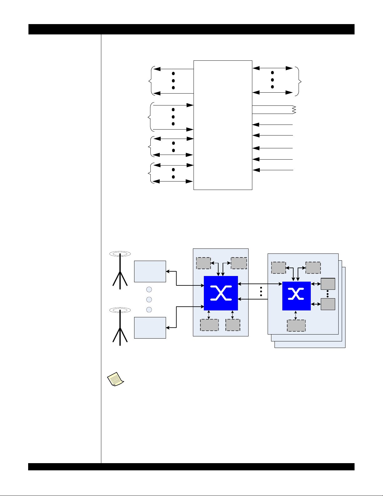
The CPS device functionality is optimized for line card and backplane switching. Its primary function is to
switch data plane and control plane data packets via Serial Rapid IO (SRIO) between a set of devices that
reside on the same line card. In addition, it supports the ability to bridge communications between multiple
on-board (or local) devices and a set of external line cards by providing long run Rapid IO backplane interconnects. In this manner, for example, the device can serve as a switch between a set of RF cards and a
set of Rapid IO based DSPs in a wireless basestation.
The CPS device supports packet switching from up to 16 ports which are comprised of 16 SRIO Lanes. The
encoded data rate for each of the lanes are configurable to either 1.25 Gbps, 2.5 Gbps, or 3.125 Gbps. The
device supports lane grouping such that both 1x and 4x operation, as defined in the applicable RIO specifications. In addition, the device supports lane grouping in an “enhanced” mode such that a group of 4 Lanes
can be configured as four individual non-redundant 1x ports.
The CPS device supports the reception of SRIO maintenance packets (type 8) which are directed to it (i.e.
hop count of 0) in support of requirements defined for a RIO switch in the applicable version 1.3 Rapid IO
specifications. The CPS device supports the ability to properly process and forward received maintenance
packets with a hop count >0 as defined in the Rapid IO specifications. With the exception of maintenance
packets, received packets are transmitted unmodified as defined in the 1.3 versions of the applicable Rapid
IO specifications.
From a switching perspective the device functions statically. As such, all input to output port mappings are
configurable through registers. Unless register configurations are changed, the input to output mappings
remains static regardless of the received data (disregarding errors). The switching functionality does not
dynamically “learn” which destinationIDs are tied to a given port by examining RIO header fields and
dynamically updating internal routing tables.
The device supports priority levels 0 - 3 as defined in the revision 1.3 Rapid IO specifications.
The CPS device is programmable by RIO ports, I
2
C JTAG interface.
CPS-16/12/8 User Manual 1 - 1 July 10, 2012
Revision 1.5
Integrated Device Technology, Inc.
Page 12

IDT Device Overview
1.2 KEY FEATURES
Interfaces - sRIO
– Up to 16/12/8 Serial RapidIO (sRIO) v1.3 full duplex lanes, supporting 4x-ports, 1x-ports, or combi-
nations thereof
– Lane Rates selectable; 3.125Gbps, 2.5Gbps, or 1.25Gbps
– Short- or Long-haul reach for each Lane at all rates
– Both pre-emphasis and drive strength
– Software assisted error recovery supports hot swap
Interfaces - I2C
– A single I
2
C interface either in master mode or slave mode
– Hardware pin configurable address
– Power up booting from external I
Switch
2
C memory device with error checking and reporting
– Peak throughput 40Gbps (CPS-16), 30Gbps (CPS-12), and 20Gbps (CPS-8)
– Support cut-through mode
– Per priority buffering
– Support 4 RIO priorities
– Non head of line blocking
– Support Multicast control symbol
– Support Broadcast
– 10 Multicast mask
– Per port independent routing table
Packet Trace
– Each Port provides the ability to match the first 160 bits of any packet against up to four program-
mable values as comparison criteria to copy the packet to a programmable output trace port
Clock and reset
– Single input reference clock
– Global hardware reset
– Software reset
Diagnostic packet counters
Power Dissipation
– CPS-16 maximum power consumption is 3.2W
– CPS-12 maximum power consumption is 2.8W
– CPS-8 maximum power consumption is 2.4W
Full JTAG Boundary Scan Support (IEEE1149.1 & 1149.6)
Package:
– FCBGA 324-ball grid array, 19 mm x 19 mm, 1.0 mm ball pitch
1.3 ADDITIONAL RESOURCES
In addition to this User’s Reference Manual, which explains the functionality of the CPS and how to use the
device. There is the device’s datasheet which covers all electrical specifications, package pinouts, and thermal characteristics available on IDT’s secure access site. Contact your local IDT sales representative to
obtain your copy.
CPS-16/12/8 User Manual 1 - 2 July 10, 2012
Revision 1.5
Integrated Device Technology, Inc.
Page 13

IDT Device Overview
Register
File
Maintenance
&
Error
Management
JTAG
I2C
SRIO
Quad 0
Logical
SRIO
SERDES
Lane 0
SRIO
SERDES
Lane 1
SRIO
SERDES
Lane 2
SRIO
SERDES
Lane 3
SRIO
Quad 1
Logical
SRIO
SERDES
Lane 4
SRIO
SERDES
Lane 5
SRIO
SERDES
Lane 6
SRIO
SERDES
Lane 7
SRIO
Quad 2
Logical
SRIO
SERDES
Lane 8
SRIO
SERDES
Lane 9
SRIO
SERDES
Lane 10
SRIO
SERDES
Lane 11
SRIO
Quad 3
Logical
SRIO
SERDES
Lane 12
SRIO
SERDES
Lane 13
SRIO
SERDES
Lane 14
SRIO
SERDES
Lane 15
1.4 BLOCK DIAGRAM
Figure 1.1 Block Diagram
CPS-16/12/8 User Manual 1 - 3 July 10, 2012
Revision 1.5
Integrated Device Technology, Inc.
Page 14
IDT Device Overview
CPS
SRIO Tx
Differential
x16
SRIO Rx
Differential
x16
I2C Interface
14 Signals
SERDES
Drive Bias
12 K ohm
RIO
Speed
Select
JTAG
Reset Signal
System
Clock
Te st
Signals
(or x8, x12)
(or x8, x12)
RF Element
RF Element
CPU FPGA
CPS-16
Serial RapidIO
CPS-8
Serial
RapidIO
DSP
DSP
CPU FPGA
1
PROM
Central Switch Board(s)
I
2
C
PROM
I2C
Baseband Board(s)
DSP
1
2
… N
Figure 1.2 CPS Interconnect
1.5 APPLICATION EXAMPLE: THE WIRELESS BASESTATION
Central switch based wireless processing
Figure 1.3 Application Overview
In a macro wireless station, a switch-based raw data combination and distribution architecture is widely
adopted. Switch based architecture provides high flexibility and high resource efficiency. The raw data from
the Radio Unit is distributed to one or more processing cards by unicast or multicast. Aggregating raw data
from processing cards to a buffer-less chain can be done by a fast non-blocking switch. It’s also suitable in
The CPS provides direct support for backplane connections using the serial RapidIO standard.
The addition of an appropriate bridge (e.g., CPRI to sRIO) allows for further backplane flexibility,
accommodating designs based on a wide range of standards such as CPRI, OBSAI, GbE, or
PCIe.
processing card since more and more processing is moved from RNC to Node B in the emerging applica-
CPS-16/12/8 User Manual 1 - 4 July 10, 2012
Revision 1.5
Integrated Device Technology, Inc.
tions.
Page 15

IDT Device Overview
1.6 FUNCTIONAL OVERVIEW
The user may program IDT’s CPS to direct incoming packet data with a given destination ID to a packet
processor. Input packets are switched as defined by the transport layer of RIO specification. The CPS
receives the packets from up to 16 unique ports, the received packets may be processed in three ways:
a. Multicast:If a Multicast ID is received, the CPS performs a multicast as defined by the
device’s configurable RIO multicast mask registers.
b. Unicast: it is performed as specified in RIO.
c. Maintenance packets: As specified in sRIO
1.7 FUNCTIONAL DIFFERENCES WITH PPS-GEN2 (80KSW0001)
1.7.1 Enhanced Queue
It can bypass the congested head in the queue.
1.7.2 Port/Lane Count
The CPS family device provides 16/12/8 sRIO lanes which can be configured into up to 16/12/8 ports. The
80KSW0001 provides up to 12 ports
1.7.3 Bandwidth
CPS provides a 40/30/20 Gbps bandwidth.
1.7.4 PPSc Capability
The CPS family does not have PPSc
1.7.5 I2C Interface
The CPS I2C interface may work either in Master mode or Slave mode.
1.7.6 Broadcast and Broadcast Packet Filtering
The CPS support broadcast and broadcast filtering.
1.7.7 Multicast Control Symbol
The CPS can distribute multicast control symbol to all other port when a multicast control symbol is
received. It enhances all out put port synchronization.
1.7.8 Software Assisted Error Recovery
The CPS can generate link request control symbol, reset control symbol and change the inbound and
outbound AckID for hot swap applications.
1.7.9 Enhance Packet Tracking
Ability to track up to 8 packets from a given input port.
1.7.10 Support for Two Separate Port Rates for Each Quad
In the same enhanced quad, different lane may run at different speed.
CPS-16/12/8 User Manual 1 - 5 July 10, 2012
Revision 1.5
Integrated Device Technology, Inc.
Page 16

Chapter 2
sRIO Ports
2sRIO PORTS
2.1 sRIO PORT DEFINITION
The CPS provides a total of 16/12/8 Serial RapidIO lanes which are configurable into combinations of 4x
and 1x ports. Each lane supports both long- or short-haul serial transmission (as defined by version 1.3 of
the Serial RIO specification).
2.1.1 Port Types
The CPS groups lanes in counts of 4 in a compatible implementation with that of the existing CPS device. A
group of 4 lanes are defined as a “Quad”. The baseline device configuration provides 4 “enhanced” Quads.
An Enhanced Quad is capable of operation in “enhanced mode” or in “standard mode”. This mode configuration is selectable through the use Quad configuration registers. When configured in enhanced mode, the
quad supports the ability for each of its four lanes to be used as individual 1x-ports (1 lane per port). When
configured into standard mode, the quad is usable as a single 4x-port (4 sRIO lanes) or as a 1x port. When
an enhanced quad’s lanes are being used as four individual 1x-ports, redundancy as defined by the sRIO
specification is not provided.
An Enhanced Quad can be configured into either enhanced or standard mode using the mode select bit in
the QUAD_CTRL register. In Standard Mode, 4x or 1x operation is governed by the Port_Width_Overide bit
in the sRIO defined PORT_CTRL_CSR.
The complement of Standard and Enhanced Ports and Quads provided by the CPS is as shown in the
following table. This table shows the maximum complement of 16 1x-ports.
Table 2.1 Port Numbering
Lane Quad Number Quad Mode
0
1 Enhanced 1
2 Enhanced 2
3 Enhanced 3
4
5 Enhanced 5
6 Enhanced 6
7 Enhanced 7
8
0
1
Enhanced 0
Enhanced 4
Enhanced 8
Port Number
(1x Capacity)
Reset
Configuration
4 by 1x
4 by 1x
9 Enhanced 9
10 Enhanced 10
11 Enhanced 11
CPS-16/12/8 User Manual 2 - 1 July 10, 2012
Revision 1.5
Integrated Device Technology, Inc.
2
4 by 1x
Page 17

IDT sRIO Ports
Table 2.1 Port Numbering
Lane Quad Number Quad Mode
12
13 Enhanced 13
3
Enhanced 12
Port Number
(1x Capacity)
Reset
Configuration
4 by 1x
14 Enhanced 14
15 Enhanced 15
The CPS supports lane to port assignments which are numbered from lane 0 to lane 15 in ordered fashion
in groups of 4 to ports 0 through 15.
An Enhanced port is capable of either being mapped into 4 device ports (if it is configured as 4 1x types) or
a single device port (if it is configured as one 4x-port or one 1x-port).
The table below is informational and shows examples of configurations with various 1x and 4x device port
complements versus link usage.
Table 2.2 Port Configuration Examples
4x Ports 1x Ports Total Lanes Used Quad Configurations
4 0 16 1 by 4x (4 total)
3 1 16 1 by 4x (3 total)
1 by 1x (1 total)
3 4 16 1 by 4x (3 total)
4 by 1x (1 total)
2 8 16 2 by 4x (2 total)
4 by 1x (2 total)
1 12 16 1 by 4x (1 total)
4 by 1x (3 total)
1 3 16 1 by 4x (1 total)
1 by 1x (3 total)
0 16 16 4 by 1x (4 total)
2.1.2 Data Rates
Each CPS sRIO Link is capable of full functionality at configurable rates of 1.25 Gbps, 2.5 Gbps, and 3.125
Gbps as defined in the Serial RapidIO Specifications revision 1.3.
2.1.3 Lane Configuration
SRIO lane characteristics is configurable via a set of QUAD_n_CTRL registers. These characteristics
include the following:
-- Data Rate
-- Transmitter Pre-emphasis
-- Drive Strength
For the CPS device, control of each of these parameters are separately configurable, such that the characteristics for lanes 0 and 1 can be different from those for land 2 and 3
CPS-16/12/8 User Manual 2 - 2 July 10, 2012
Revision 1.5
Integrated Device Technology, Inc.
Page 18

IDT sRIO Ports
In addition, these registers supports the ability to reset lanes in the quad and to force a reinitialization of
lanes in the enhanced quad. The ability to control reset and initialization of lanes 0 and 1 versus lanes 2 and
3 through these registers are also provided.
2.1.4 Packet Forwarding
2.1.4.1 Store and Forward
CPS supports a “Store and Forward” methodology for packet forwarding. This methodology consist of validation of each received packet to the SRIO specifications (including a successful CRC verification) before
the packet is forwarded via the output port referenced by the destination ID in the packet header.
2.1.4.2 Cut Through
CPS supports “Cut Through” packet forwarding methodology. This methodology provides the ability to
begin forwarding a packet via its referenced output port before it has been validated. Packets that have
been found to be invalid after transmission has begun, is terminated with the SRIO STOMP control symbol
which will be used in compliance with the rev 1.3 SRIO protocol standard. Assuming no starvation and no
output port contention, the first byte in to first byte out latency for a maximum sized packet will be the same
as that for a minimum sized packet.
Packet counters are implemented such that packets which are STOMPED are not included in the count.
Note that Cut Through mode supports the use of the retransmit buffer for reliable transport as defined in the
SRIO protocol specification.
If a Cut Through packet is being transmitted and the transmission becomes starved for data (part of the
packet has been transmitted but the rest of the packet is not available for transmission) EOP control symbol
will be transmitted within the packet (i.e within the boundary of the packet’s SOP and EOP) until the rest (or
more) of the packet becomes available for transmission.
Cut Through is disabled at reset of the device. This mode is enabled globally via a maintenance write
command to the CUT_THRU_ENABLE bit of the CPS_CONTROL register. If this bit is set, Cut Through
forwarding methodology will be enabled for all CPS ports.
When Cut Through is enabled the devices’ output packet scheduler will consider a packet as available for
transmission/forwarding as soon as enough of the packet (i.e. the destination ID has been received and
decoded) to determine which port to use for transmission. The device does not use full packet reception as
a criteria to determine when a packet is available for transmission.
2.1.5 Port Statistics (Packet Counter)
The CPS provides the ability to generate statistics at each port. Each port provides a 32-bit packet counter
for each of the following data at that given port:
1) Ack Counter: Number of Packet-accepted control symbol has been sent; number of packet has
been successfully received.
2) Nack Counter: Number of Packet-not-accepted control symbol and packet-retry control symbol
sent. Note, during the initialization and re-initialization, it may cause some Nack count. User should
clear the Nack count after port initialization.
3) Switch Counter: Number of packets successfully sent out
3) Trace Counter: Packets which have met port’s trace criteria (when enabled)
4) Filter Counter: Packets which have been filtered
All counters will reset to 0 when read, and will hold their maximum value (saturate) when it is reached.
2.2 TRACE FUNCTION
Each port supports the ability to compare a configurable set of parameters in a given received packet
against a set of configurable predefined values and, if a match occurs, routes the packet to a configurable
output port. This function is defined as the “Trace” function.
CPS-16/12/8 User Manual 2 - 3 July 10, 2012
Revision 1.5
Integrated Device Technology, Inc.
Page 19

IDT sRIO Ports
Packet Data
bit
0
..............................................bit
n<160
bit
0
........................................................................................bit
160
Comparison Data
Comparison Mask
bit
0
..............................................bit
n<160
X
n+1
................................X
160
X = don’t care
The device supports the ability to route a packet which matches the “Trace Criteria” to the port referenced
by the packet’s destination ID (including multicast references) as well as to the trace port.
Each port provides a unique trace circuit such that the user may enable trace on up to 16 simultaneous
ports (4 for each of the 16 ports) as defined below.
2.2.1 Trace Criteria
The property of a given port matching a packet with a “Trace Criteria” refers to a successful comparison of
the first 160 bits in a received packet to multiple pre-programmed values stored at that port. A successful
match against a port’s Trace Criteria triggers a forwarding of the packet to the trace enabled output port.
Each port provides a set of four 160-bit comparison values which can be selectively applied to the first 160
bits of each packet that the port receives. Each port also provide a bit mask for each of the four programmable 160 bit comparison values which define which of the first 160 bits of packet data are relevant to the
comparison. A logical value of 1 in the comparison value mask indicate that the corresponding bits in the
programmed value and the corresponding bit in the packet data is compared. A logical value of zero in the
comparison value mask is used as a “don’t care”. A don’t care value results in an automatic match of the
corresponding bits in the programmable value with the corresponding packet data bits. When all bits of the
packet data match with a given corresponding bit in a given programmable value (after the value’s mask
has been applied) the Trace criteria has been met and the packet is forwarded to the trace enabled output
port. The packet trace is triggered by a logical “OR” of the comparison match results (packet data with the
four programmable values) such that if at least one match occurs, packet forwarding to the trace-enabled
port is performed.
The trace criteria is based on the “entire content” of the comparison value and its corresponding
bit mask. This is true in the event that the bit count of the received packet is smaller than 160
bits. In this event, in order to match the trace criteria, the number of bits in the mask which are
greater than the received packet data must be set to don’t cares as shown below.
Figure 2.1 Trace Matching Criteria
For clarification, if the user wants to trace a packet which is smaller than 160 bits, the number of mask bits
between the packet size and 160 must be set to don’t care.
A packet which matches any of the four values are forwarded to the trace enabled output port as well as
any other ports referenced by the packet’s destination ID.
The Trace Criteria architecture is illustrated in the diagram below.
CPS-16/12/8 User Manual 2 - 4 July 10, 2012
Revision 1.5
Integrated Device Technology, Inc.
Page 20

IDT sRIO Ports
0159
RIO Packet Received
at Port n of 16
First 160 bits of packet
0 159
Programmable Comparison 0
Mask 0
Mask 1
Programmable Comparison 1
Mask 2
Mask 3
Programmable Comparison 2
Programmable Comparison 3
Trigger
0 159
0159
0 159
0 159
0 159
0 159
0 159
Figure 2.2 Illustration of the Trace Function within a Given Port
From an application perspective, the support for comparison over the first 160 bits of the packet is to ensure
that the trace function can cover the worst case RapidIO header (including those using extended
addressing) plus the first 32 bits of the payload. This implementation is totally flexible across the first 160
bits of the packet and ensures that the following parameters can be used as trace criteria: 1) the header’s
ftype field (4 bits), 2) the header’s destination ID field (8 or 16 bits), 3) the header’s mbox field (up to 8 bits),
4) the first 32 bits of the packet payload (32 bits). Note that If the input port detects an error in the received
packet it will not be routed to the trace port.
2.2.2 Trace Output Port Features
At any given time the device supports a single Trace-enabled output port. It can be dynamically defined
which output port is enabled for the Trace function. All packets which match the Trace Criteria from all trace
enabled inputs is routed to the same configured trace output port.
The device supports the ability for the port defined as the output trace port to be also part of a multicast
group. At the same time it is also possible for the user to configure the trace output port to match the
intended destination port of a packet.
The trace port needs to be disable first before changing to a new trace port.
2.2.3 Trace Routing Features
CPS routing function in support of the trace function is provided in two modes.
CPS-16/12/8 User Manual 2 - 5 July 10, 2012
Revision 1.5
Integrated Device Technology, Inc.
Page 21

IDT sRIO Ports
2.2.3.1 Default Trace Routing Mode
In the default mode, the trace-enabled port accepts RapidIO traffic (referenced by the received packet’s
destination ID field) as well as traffic which matches the trace criteria of all ports. Trace-triggered packets
are treated by the trace-enabled output port in the same manner as it treats all other packets. Normal
RapidIO priority and flow control rules apply.
2.2.3.2 Optional Trace Routing Mode
In an optional mode, ONLY packets which have matched a port’s trace criteria are routed to the trace port.
For switch path, a received packet which does not match the Trace criteria, but whose destination ID field
references the Trace-enabled port is not forwarded to the trace port. If this packet has a destination ID that
references a multicast operation that includes the trace port, the packet is forwarded to all ports except for
the Trace-enabled port. However, packets from maintenance are still sent to the trace port even the packet
does not match trace criteria. Trace-triggered packets are treated by the trace-enabled output port in the
same manner as it treats all other packets. Normal RapidIO priority and flow control rules apply.
It is possible to configure the trace port into “trace only” mode and at the same time for the user to configure
a port’s route table to allow packets to be routed to the trace port (including packets which do not match the
trace criteria). With this configuration, packets received by a given port which are to be routed to the trace
port (as defined by that port’s route table) will be dropped by the device if they do not match the trace
criteria.
2.2.3.3 No Route Conditions
Packets which meet the trace criteria are routed to the trace port even if the packet destination ID reference
in the port’s route table indicates “no route”.
2.2.4 Trace Function Dynamic Programmability
By offering dynamic configurability, the CPS device provides the user with the ability to modify trace function parameters without disabling the normal operation of the port’s functionality.
The user is able to:
1) dynamically enable/disable the Trace function on a per-input port basis
2) dynamically assign the trace output port to any single output port
3) dynamically change the packet trace comparison values of any port
4) dynamically enable/disable any/all trace comparison values of any port
5) dynamically change the comparison value masks at any port
6) change a comparison value or mask (same value) for all ports with a write to a single address
2.2.5 Test feature for Trace Function
Each port provides a set of counters which increment each time the given port receives a packet that
matches the Trace criteria. Each port provides a counter for each of the four comparison values. These
counters are accessible in the same manner that all other device counters are made accessible. All trace
counters are 32-bits.
2.2.6 Flow Control with Trace Enabled
The CPS supports sRIO defined receiver flow control when Trace is enabled as well. If buffer contention
exists at the trace port such that a received packet which matches a port’s trace criteria would have to be
dropped (and therefore not be transmitted via the trace port) then the received packet is NACKed by the
port. If this condition exists the packet is not transmitted by any port regardless of its buffer condition. For
example, if the trace output port can’t receive additional packets because of buffer congestion, but there is
buffer space to support the normal (non-trace) path through the device, then the packet must be NACKed
and NOT transmitted via the normal route output port.
CPS-16/12/8 User Manual 2 - 6 July 10, 2012
Revision 1.5
Integrated Device Technology, Inc.
Page 22

IDT sRIO Ports
2.2.7 Errored Packets
The device does not trace packets with physical errors such as packet with CRC errors and packets that
are longer than 276 bytes. The device traces packets with logical errors (ex. invalid type) as long as they
match the trace criteria.
2.2.8 Trace Configuration
The Trace Function is enabled globally for the device with a write to the CPS_CONTROL register. When
global trace is enabled the Trace Output Port defined in the CPS_CONTROL register will be enabled. The
CPS_CONTROL register is used to control the mode of the Trace Output Port (Default or Trace only).
Each port supports an enable of each of its four trace criteria values in its respective PORT_n_OPS
register. This will be independent such that a match on any given value does not depend on a match of any
other value. The PORT_n_OPS register will also control whether or not a packet that matches a given port’s
trace criteria will cause the device to generate a Port Write packet.
2.2.9 Cut Through with Trace
The device supports Cut Through when Trace is enabled (see section 2.1.4.2).
2.3 PACKET FILTERING
Along with the ability to trace packets via comparisons against up to four comparison values, the CPS
device supports the ability to filter packet based on comparisons against these same values. If this packet
filtering is enabled, a successful comparison of the first 160 bits in a received packet to a port’s preprogrammed values will result in the packet being dropped or “filtered” by the device. Note that a successful
comparison will also prevent a maintenance packet from being “accepted/processed” by the CPS device (in
the event that a maintenance packet that met the filter criteria had a hop count of 0).
The device supports the ability for the packet filtering to be enabled/disable at each port individually for
each unique comparison value at that port.
The device provides the ability to enable/disable packet trace and packet filtering simultaneously for each
port individually for each unique comparison value at that port. If both packet filtering and packet trace are
enabled and a match occurs between a received packet and a comparison value, then the packet will be
dropped but will also be traced to the specified trace output port. If packet filtering is enabled but trace is
not, then the packet will be filtered and not traced to the specified output trace port.
In the case where packet does not match the filter and TRACE_OUTPUT_PORT_MODE is set
to a 1, the packet will not be routed to the destined port. IDT recommends to set the
TRACE_OUTPUT_PORT_MODE to 0 when only packet filtering is enabled.
The device provides a counter at each port for each comparison value. The counter provides a continuous
count of the number of packets that have been filtered at each port as a result of a successful match against
each comparison value.
2.4 SOFTWARE ASSISTED ERROR RECOVERY
Each port supports the software assisted error recovery registers defined in the rev 1.3 revision of the SRIO
specification. Specifically these registers include the Port n Link Maintenance CSRs, the Port n Link Maintenance Response CSRs, and the Port n Local ACKID CSRs. A set of each of these three registers are
provided per port.
2.4.1 Usage Definition for Port n Link Maintenance CSRs
A write to these registers will force CPS to transmit a Link Request Symbol on the associated link. The
command field in the transmitted symbol will be the contents of the command field written into this register.
A read of this register will return the value of the command field in the register.
Support is provided for two command field values: 1) Reset (0b011), and 2) Input Status (0b100)
CPS-16/12/8 User Manual 2 - 7 July 10, 2012
Revision 1.5
Integrated Device Technology, Inc.
Page 23

IDT sRIO Ports
2.4.2 Link Maintenance CSR Reset Command field
A write to the Port n Maintenance CSR with the command field set to 0b011 (reset) the device will:
1) cease all current and pending transmissions (data and SRIO control symbols -- including multicast control symbols),
2) transmit 4 link request -- reset symbols in succession. After transmitting the link request -- reset
symbols, the port will enter the output error state and wait for a corresponding link response.
2.4.3 Usage Definition for Port n Link Maintenance Response CSRs
The Port n Link Maintenance Response CSRs will be read only registers which contain the information
contained in the most recently received link response by the specific port. When read, it will return the data.
2.4.4 Usage Definition for Port n Local ACK ID CSRs
The CLR_OUTSTANDING_ACKIDs, INBOUND_ACKID, OUTSTANDING_ACKID, & OUTBOUND_ACKID
fields defined for this register are supported.
2.4.4.1 CLR_OUTSTANDING_ACKIDs
This single bit field will be treated as write only. When this bit is written to a value of 1, CPS treats all previously transmitted packet for which acks have not been received as having been properly received by the
link partner. Acknowledgment processing for these packets will no longer be required.
2.4.4.2 INBOUND_ACKID
CPS supports both reads from and writes to the INBOUND_ACKID parameter. If read, CPS will return the
value of the expected ack ID of the next received packet.
A write of this parameter will set the expected ack ID for the next received packet to the value supplied with
the write. If the port receiver state machine is in a stopped state it will return to the normal operational state
after updating the expected ID value. If a packet is being received during this transition, it will be dropped
without response.
2.4.4.3 OUTBOUND ACKID
CPS supports both reads from and writes to the OUTBOUND_ACKID parameter. If read, CPS will refer to
the value that the device will use for the next transmitted packet ack.
If written, the effect will be dependant upon whether or not there are outstanding ackIDs. If there are no
outstanding ackIDs, the next transmitted packet will use the ackID written into this register. If there are
outstanding ack IDs, the packets that have been previously transmitted (without the device having received
an acknowledgement), will be retransmitted using ack IDs which start from the value written into this
register.
2.4.4.4 OUTSTANDING ACKID
CPS supports both reads from and writes to the OUTSTANDING_ACKID parameter. If read, this parameter
will indicate the value of the next expected acknowledgement (control symbol ack ID field) from the port’s
link partner. The effect of writing this parameter will depend upon the current state of the port’s outstanding
ack ID status as follows:
1) If the port has no outstanding ack IDs the write will have no effect on the port. Because of the
Outstanding AckID always reflects the ackID that the port expects to received next, so if the outbound ID change, then the outstanding ID will be changed.
2) If the port has outstanding ack IDs and the written value is one of them, the port will accept all
existing ack IDs with lower values. Which means the port will accept the existing packets with this
written value ackID and following values. The write in this case will have no effect on the ack ID of
the next packet to be transmitted.
3) If the port has outstanding ack IDs and the written value is not one of them an error will be
recorded and the port will take no action.
CPS-16/12/8 User Manual 2 - 8 July 10, 2012
Revision 1.5
Integrated Device Technology, Inc.
Page 24
Chapter 3
Switch Description
3 SWITCH DESCRIPTION
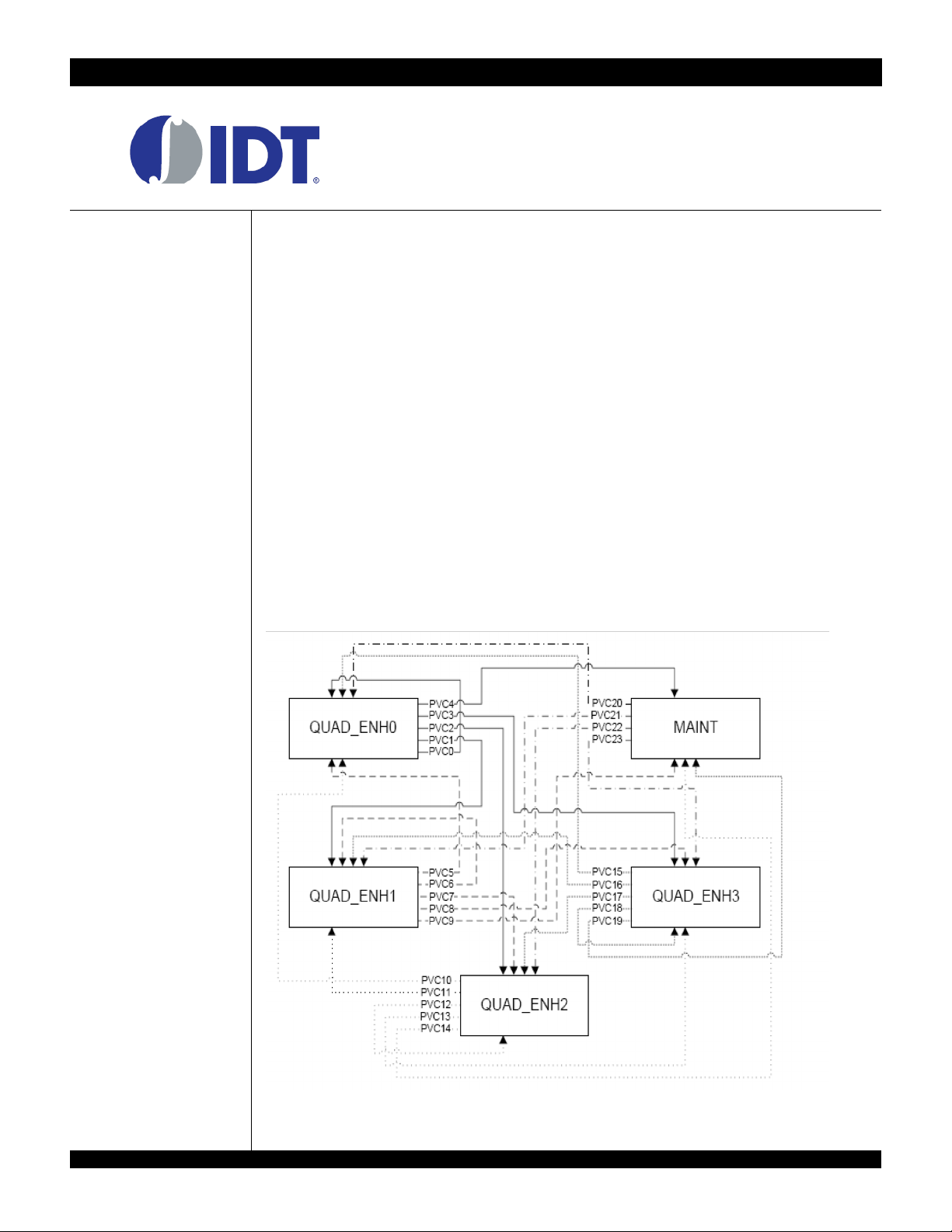
3.1 CONCEPTUAL FUNCTIONALITY
The CPS pseudo mesh architecture is a combination of full mesh and TDM. The architecture is intended to
avoid numerous parallel data paths within the switch, as opposed to a centralized arbitration scheme.
Permanent Virtual Circuits (PVC) connections supports 10Gb/s of unidirectional data traffic. In systems
where the QUAD_ENH modules are operating as a single port with a maximum data bandwidth of 10Gb/s
then the PVCs connected to each quad is dedicated to supporting that port. In systems where the
QUAD_ENH modules are operating as 4 independent ports each with a maximum 2.5Gb/s data bandwidth,
the PVCs connected to that quad supports all 4 ports by granting bandwidth to each port in 32bit (word)
portions. It is this time sharing concept that is the origin of many of the sub-modules that refer to time division multiplexing (TDM) in regard to PVC operation. This TDM method is strictly per PVC and is not functional as an overall switch-wide time division scheme. The packet ordering and sRIO protocol enforcement
is handled in a distributed nature as well. The CPS switch core acts like a three stage switch composed of
TDM, full mesh and TDM.
3.2 SWITCHING BLOCK AND ELEMENTS
The block diagram of the figure below shows the topology of the CPS Switch architecture. The PVC
acronym refers to the interconnections illustrated in the figure which may be considered as permanent
virtual channels. Inside each QUAD, TDM connects each port to PVC.
Figure 3.1 CPS Switch Core Block Diagram
CPS-16/12/8 User Manual 3 - 1 July 10, 2012
Revision 1.5
Integrated Device Technology, Inc.
Page 25
IDT Switch Description
1
2
3
14
:
140B
Priority0
28B
pack et
1
st
packet
2nd
packet
1
2
3
14
:
140B
Priority0
28B
pack et
1
st
packet
2nd
packet
3.3 SWITCH DESCRIPTION
The CPS device consists of three parts; the input buffers, the switching core, and the output buffers. Each
of the three portions of the switch will be described in further details in the following sub-sections.
3.3.1 Input Buffers
There are separate buffer resources for maintenance packets and data packets. This effectively allows a
separate maintenance path through the switch. With judicious use of priorities, user can guarantee
minimum latency through the system for maintenance packets even when data packets are congesting at
these same ports.
For data packet, there is buffer space with room for 7 max size packets (1960 Byte) for each of the ports on
the device. The port buffer space can be allocated through registers to the four priority levels, and can be
configured on a per port basis. There will always be allocated room for at least one full size packet for each
priority level. The buffer space is allocated in units of 35 word (140 Byte), so 2 units are required for storing
one full maximum sized packet. The default buffer setting is 4 max size packets for priority 0 and 1 max size
packet for all other priority. The recommended allocation of buffer space is 3 maximum size packet for
priority 0, 2 maximum sized packets for priority 1, and 1 maximum sized packet for priority 2 and 3, but this
is subject to change by user. The input buffer simply provides a temporary storage for incoming packets
and absorbs the burst.
For maintenance packet, the buffer size is 88Bytes per priority per port. Separate maintenance packet input
buffer will avoid being blocked due to resource sharing.
For each priority of a specific port, the input buffers can keep track of up to 4 or 8 packets, giving that there
is enough buffer space to hold them. The EXTENDED_PKT_RX_ENABLE bit in Port Operation register
selects the number 4 or 8. See 3.3.3 Extended Packet Tracking.
When a packet arrives it will only be accepted into an input buffer if that buffer has room for at least one
data word of 32 bits, for each additional data word of the packet if there is no more room in the buffer the
packet will be aborted and a RETRY will be sent back out on the sRIO link. See Figure below.
Figure 3.2 Input Buffer Diagram
3.3.2 Extended Packet Tracking
CPS-16/12/8 User Manual 3 - 2 July 10, 2012
Revision 1.5
Integrated Device Technology, Inc.
The extended packet tracking function allows input buffer keep track up to 8 packet per priority. (See
register 0xF40004 bit 18). It is typically for small packet application. When the extended packet tracking
function is enabled, the non-blocking within the priority function will be disabled automatically.
Page 26

IDT Switch Description
3.3.3 Switch Core
The switch core acts like a three stage switch composed of TDM, Mesh and TDM. Full mesh PVC connects
QUAD to QUAD, and QUAD to maintain block as well, TDM connect Ports to PVCs.
3.3.3.1 QUAD to QUAD Full Mesh PVC
The PVC module is used to connect every quad to every other quad as well as all quads to the maintenance handler and the maintenance handler to all quads. It handles data transfer as well as control. The
PVC module serves as a pipeline connection between nodes. It provides no other functionality beyond this
and simply made up of registers for all incoming signals that then drive the outputs. It has all the advantages of full mesh.
3.3.3.2 PORT to PVC TDM
Inside each QUAD, the PORTs are connected to PVC network in TDM manner. It is this time sharing
concept that is the origin of many of the sub-modules that refer to time division multiplexing (TDM) in regard
to PVC operation. This TDM method is strictly per PVC and is not functional as an overall switch-wide time
division scheme.
3.3.4 Output Buffers
There are separate output buffer resources for maintenance packet and data packet. The output buffer
provides a temporary storage for outgoing packets, it decouples the switching and transmitting. It achieves
wire speed while transmitting different priority packets per sRIO specification.
For data packet path, the output buffer size is 448 bytes per priority per port. Each output buffer can track
up to 3 packets, given that there is enough buffer space for them. The output buffer will only allow new
packet in if it has free tracking resources and buffer space available for a full maximum sized packet.
For maintenance packet path, the buffer size is 88 bytes per priority per port. The separate maintenance
packet buffer forms an independent data path.
3.3.5 Retransmit Buffers
There is 4-max-packet-size retransmit buffer for each priority for a given port. For a given port, there is
totally 16 max-packet-size buffer. Each priority can keep track of up to 32 packets. Both data packet and
maintenance packet share the same buffer. The retransmit buffer is enough to deal with normal response
delay.
3.4 SWITCHING SCHEDULER AND PRIORITIES
3.4.1 Input Buffer to Output Buffer
First arrive first served is the basic rule of moving data from input buffer to output buffer. For the same
source port, strict-priority is applied. That means packets in the higher priority queue always is served first.
For a given queue of given source port, it can bypass the destination-blocked packet to serve subsequent
packets. Maintenance packets are always treated as higher priority than data packet.
For the same destination, same priority, different sources to this destination are done in a Round-Robin
manner.
These rules apply to multicast and unicast. The difference is that the input buffer will not be released until
the packet has been forwarded to all destinations in the multicast list. In another words, one blocked destination port of the multicast list will not block the forwarding to other destination ports (multicast splitting), but
it does hold the input buffer resource.
CPS-16/12/8 User Manual 3 - 3 July 10, 2012
Revision 1.5
Integrated Device Technology, Inc.
Page 27

IDT Switch Description
3.4.2 Output Buffer to Transmit Buffer and Transmit Buffer to Line
3.4.2.1 Unicast Packets
If a tx port fails in an attempt to transmit a priority N packet (call it PA) due to CRC error, and there is a
priority >N Packet (call it PB) available at the port’s retransmit buffer, then that higher priority packet PB
must be the next one sent. Specifically, if tx port A transmits a packet of priority N (call it PA) but receives a
“not accepted” response, then the next packet transmitted after receiving the response must be a packet of
priority > N if one is available in the retransmit buffer. Since the “not accepted” result is due to CRC error,
then the original packet PA will be retransmitted up to X times (See port operation register, bit 3-1, number
of retransmissions). Before each of the X attempts, the retransmit buffer will be reviewed to verify that there
are no priority > N packets available. If after X attempts the original packet PA is still not accepted, then PA
will be discarded and transmission of the next packet in tx port A’s retransmit buffer will be attempted. If the
“not accepted” cause by the traffic flow control such as the endpoint is busy or endpoint input buffer is full,
then PA will remain in retransmit buffer and keep retransmit until PA pass through. The following is standard
behavior:
1) The retransmit buffer must have room for at least one maximum size packet of each of the four
priorities. If the highest priority packet in the retransmit buffer is priority N, then the retransmit buffer
must reserve space sufficient to store at least S maximum size packets, where S = 3-N. The minimum size retransmit buffer that can meet this requirement is 4 times the maximum packet size.
2) If the highest priority packet in the retransmit buffer has priority N, and a packet of priority > N is
being offered to the retransmit buffer by the switch's TXBUFs, then the retransmit buffer must
accept the packet from the TXBUFs. This is true even if the tx port is blocked by a packet of priority
N or less.
3) If TX/RX BUFs has lower priority packet A in buffer and continuously received higher priority
packet which reach the port bandwidth, then the lower priority packet will continuously hold off until
higher priority packet bandwidth drop below the port bandwidth. The same rule apples to all ports.
Also, the following behavior is standard:
1) Not blocking with the same priority. If rx port B receives a packet (call it PC) of priority M
(where M <= N) targeted for tx port A, but port A cannot receive it due to the conflict resulting from
PA described above, then PC will remain in the input buffer. All subsequent packets received at rx
port B of priority M or higher targeted for other tx port will still switch over. For the subsequent
packet with priority < M targeted for ANY tx port will delayed until packet PB can be forwarded to
the switch.
3.4.2.2 Multicast Packets
In general, multicast packets will be treated similarly to unicast packets. Specifically, if tx port A transmits a
multicast packet of priority N (call it PA) but receives a “not accepted” response, then the next packet transmitted after receiving the response must be a packet (unicast OR multicast) of priority > N if one is available
in the retransmit buffer. If the “not accepted” cause by the CRC error, then the original packet PA will be
retransmitted up to X times (See port operation register, bit 3-1, number of retransmissions). Before each of
the X attempts, the retransmitted buffer will be reviewed to verify that there are no priority > N packets available. If after X attempts the original packet PA is still not accepted, then PA will be discarded and transmission of the next packet in tx port A’s retransmit buffer will be attempted. If the “not accepted” cause by the
traffic flow control such as the endpoint is busy or input buffer is full, then PA will remain in retransmit buffer
and keep retransmit until PA pass through. The following is standard behavior:
1) The retransmit buffer must have room for at least one maximum size packet of each of the four
priorities. If the highest priority packet in the retransmit buffer is priority N, then the retransmit buffer
must reserve space sufficient to store at least S maximum size packets, where S = 3-N. The minimum size retransmit buffer that can meet this requirement is 4 times the maximum packet size. It is
not necessary to distinguish between unicast and multicast packets in filling these buffers. They
may be filled with 4 unicast packets, 4 multicast packets, or any combination of unicast and multicast packets.
CPS-16/12/8 User Manual 3 - 4 July 10, 2012
Revision 1.5
Integrated Device Technology, Inc.
Page 28

IDT Switch Description
2) If the highest priority packet in the retransmit buffer (unicast OR multicast) has priority N, and a
unicast or multicast packet of priority > N is being offered to the retransmit buffer by the switch's
txbuf, then the retransmit buffer must accept the packet from the TXBUFs.
Also, the following behavior is standard:
Multicast Split: If rx port B receives a packet (call it PC) of priority M (where M <= N) tar-
geted for tx port A, but port A cannot receive it due to the conflict resulting from PA described
above, then PC will remain in the input buffer but it will continue multicast to other available tx
port. All subsequent packets (multicast or unicast) received at rx port B with priority => M targeted for other tx port will still switch over. For the subsequent packet with priority < M targeted
for ANY tx port will delayed until packet PB can be forwarded to the switch. PC will not remove
from the input buffer until port A is available to receive new packet.
For multicast, sRIO specification is limited to request transactions that do not require responses,
such as SWRITE transactions. So it is user’s responsibility to multicast non-response packet.
The CPS will blindly forward packet based on the ID and routing table. If user multicast a transactions with responses, the CPS will not drop any response. All responses will forward to the
sender base on the DestID.
3.4.2.3 Re-Transmission MIMIC
The intent of RT-mimic was to allow for streaming data application where low-latency is preferable even at
the cost of occasional packet loss. It is implemented by not storing packets in the retransmit buffer. In this
way, if a retry was received because the link partner has a full input buffer or if a NAK was received because
of a transmission error, then CPS would simple resent the next available packet instead of retransmitting
the previous one. RT-mimic affects behavior on the output-port only and all packet traffic if it is enabled.
3.5 FLOW CONTROL AND CONGESTION MANAGEMENT
3.5.1 Flow Control Internal
Internally, self defined protocol coordinate each module. The flow control is always companioned with data
in the anti-direction. Data is moving from input buffer to output buffer, flow control is send from output buffer
to input buffer. Quick transportation and quick response minimize the buffer dimension.
3.5.2 Flow Control External
The CPS family SRIO port supports receiver based flow control. (See sRIO spec for detail information
about receiver based flow control)
CPS-16/12/8 User Manual 3 - 5 July 10, 2012
Revision 1.5
Integrated Device Technology, Inc.
Page 29

Chapter 4
I2C Interface
4I2C Interface
This chapter discusses the I2C capabilities of the CPS-16/12/8.
4.1 Overview
The I2C Interface is compliant with the I2C Specification as a slave device and as a temporary master. The
2
I
C port can be thought of primarily as a control plane access point for the CPS-16/12/8. An external device
such as a host processor can use it to access the CPS-16/12/8’s registers. The port can also be used by
the CPS-16/12/8 to load registers.
The use of the I
RapidIO ports. There is no special safeguard on the I
should assign the I
4.2 Master/Slave Configuration
2
C port is not targeted as a bridge to other external devices through the CPS-16/12/8’s
2
C address as per specification.
2
C address assignment inside the device. Users
The CPS-16/12/8 provides an external signal, MM, to configure the device in Master mode or Slave mode
out of reset. When this signal is tied to V
(1.2V), it configures the device into temporary Master mode
DD
after reset. If left floating, it will configure the device into Slave mode after reset.
4.3 Temporary Master Mode
The CPS-16/12/8 supports temporary Master mode to directly obtain its configuration from an external
EEPROM using I
registers from an external EEPROM. The CPS-16/12/8 will operate one burst read to download all data
from EEPROM. I
The device supports configuration into temporary Master mode in two ways:
1. If an external Master mode signal is tied to V
2. If the Master mode signal is left floating the device will come out of reset in Slave mode, but can be
configured to transition to Master mode. This is done by setting I2C frequency, slave address, and
checksum disable in I2C Master Control Register and I2C Master Status and Control Register.
2
C. As such, in Master mode the device can read/download, and optionally verify, its
2
C burst read start address 0xh00 (16bit address bit).
(1.2V), the device will come out of reset in Master mode.
DD
4.3.1 Obtaining Configuration in Master Mode
If the Master mode signal, MM, is tied to VDD (1.2V), the CPS-16/12/8 will attempt to load its configuration
registers after the device reset sequence has completed. The CPS-16/12/8 uses a 7-bit address of
1010[ID2][ID1][ID0] as the slave address of the device from which it will obtain its configuration.
[ID2][ID1][ID0] are external signals to the device, and are the same three lower bits that would be used for
the device’s I
master, the device supports communication only with an external device that has a 7-bit address. 10-bit I
addressing is not supported in this mode. The data includes a CRC value that the CPS-16/12/8 uses to
compare against its own calculated value to determine the validity of the registers load. The registers are
loaded from the EEPROM regardless of the value of the checksum, but a flag is set (I2C Master Status and
Control Register.I2C_CHKSUM_FAIL) if the CRC fails.
2
C address when configured as a slave. When configured to come out of reset as an I2C
2
C
CPS-16/12/8 User Manual 4 - 1 July 10, 2012
Revision 1.5
Integrated Device Technology, Inc.
Page 30

IDT I2C Interface
When in this mode, the state of the external ADS signal is ignored. Once the CPS-16/12/8 completes its
configuration sequence (successfully or unsuccessfully), it reverts to Slave mode (where the ADS signal
becomes active).
4.3.2 Commanded Master Mode
The CPS-16/12/8 can be commanded into temporary Master mode using a maintenance write to the I2C
Master Control Register and I2C Master Status Control Register. In this scenario, the device has come out
of reset in Slave mode with the Master mode external signal left floating, or optionally tied to GND. Writing
to START_I2C_EPROM_READ in the I2C Master Status Control Register causes the device to transition
from Slave to temporary Master mode and read the EEPROM from the address specified in the
EPROM_START_ADDR.
Commanded Master mode provides more configuration sequence flexibility. In this scenario the EEPROM
slave address, and the EEPROM start address for the download, are both programmable. Whether or not a
checksum comparison is performed to validate the download is also programmable. These configuration
sequence options are established by writes to the I2C Master Control Register and I2C Master Status
Control Register.
During (and after) the configuration sequence, the CPS-16/12/8 provides status information about the
operation. This status includes whether or not any I
finished, and whether or not the operation was successful. The ability to abort the operation using a
maintenance write to the I2C Master Status Control Register is also provided.
When the device is in temporary Master mode, the state of the external ADS signal is ignored. Once the
device completes its configuration sequence (successfully or unsuccessfully), it reverts to slave mode
(where the ADS signal will become active).
2
C errors occurred, whether the operation is active or
4.3.3 Master Clock Frequency
While in the Master mode, the CPS-16/12/8 can be configured to supply a clock of either 100 kHz (Standard
mode) or 400 kHz (Fast mode).
4.3.4 Register Map
The device’s register map is based on the concept of configuration blocks whose definition and
accompanying data is located at specific places in the EEPROM address map. The definition of the register
map is as follows:
1. Byte addresses 0x0000 and 0x0001 contain the version number to be used as an initial verification of the
registers (see Table 4.1). Each address must contain the value 0xAA, otherwise the EEPROM contents
will not be loaded.
2. Byte addresses 0x0002 and 0x0003 define the number of configuration blocks that are in the register
map. This value is one less than the number of configuration blocks in the device. For one image, the
value should be 0x00 for each address.
3. Byte address 0x0004 is the start of the first block. All blocks have the same format.
4. The first byte in the block encodes the lower 8 bits [7:0] of a 10-bit word defining the number of registers
represented in this block. A value of 0 = 1 register, 1 = 2 registers, and so on.
5. The first two bits in the second byte (bits 7 and 6) are the upper two bits of the number of registers loaded.
The lower 6 bits are the upper bits of the address (bits [21:16]).
6. Bytes 3 and 4 of the block encode the address to load the data that follows. The 22-bit address is the
24-bit device register address with the lower 2 bits dropped and assumed to be zero.
7. The remainder of the bytes of the block contain the data to be loaded into consecutive register addresses.
8. Subsequent blocks use the same format, number of registers, address, and data.
CPS-16/12/8 User Manual 4 - 2 July 10, 2012
Revision 1.5
Integrated Device Technology, Inc.
Page 31

IDT I2C Interface
9. Note, registers that are only 8 bits wide will only load 8 bits of data from the EEPROM. The data for
subsequent registers will be every 8 bits.
10. The last two bytes of the register map represent the CRC for the image. For more information, see CRC
Calculation.
A tabular view of this definition is displayed below.
Table 4.1 EEPROM Register Address Map
EEPROM
Address (byte
level addresses)
Bits EEPROM Contents Comments
0x0000 0:7 First byte of Version Number [0:7] This value must be = 0xAA. The
two version bytes are used as an
early validation of the format of the
memory block. If the read value
from the EEPROM does not equal
0xAA the read configuration
sequence will be terminated.
0x0001 0:7 Second byte of Version Number
This value must be = 0xAA.
[8:15]
0x0002 0:7 First byte of a 16-bit value that
defines the total number of
configuration blocks to read [0:7]
0x0003 0:7 Second byte of a 16-bit value that
defines the total number of
For n configuration blocks, the
value entered here is n-1
configuration blocks to read [8:15]
0x0004 0:7 The lower 8 bits of a 10-bit value
that defines the number of words in
configuration Block 1.
Represents bits [0:7] of the 10-bit
block count. For m words, the value
entered here is m-1.
0x0005 0:1 Bits 8:9 of the 10-bit block count -
0x0005 2:7 Bits 0:5 of the block address -
0x0006 0:7 Bits 6:13 of the block address -
0x0007 0:7 Bits 14:21 of the block address Bits 22:23 are zero.
0x0008:0x000B All Bits 0:31 of the data to load into
EEPROM address, 0x0005 to
0x0007
0x000C:0x000F All Bits 0:31 of the data to load into the
above address + 1
... ... Remainder of block 1 -
n 0:7 The lower 8 bits of a 10-bit value
that defines the number of words in
configuration Block 2.
Represents bits [0:7] of the 10-bit
block count. For m words, the value
entered here is m-1.
n + 1 7:6 Bits 8:9 of the 10-bit block count -
n + 1 2:7 Bits 0:5 of the block address -
CPS-16/12/8 User Manual 4 - 3 July 10, 2012
Revision 1.5
Integrated Device Technology, Inc.
Page 32

IDT I2C Interface
Table 4.1 EEPROM Register Address Map (Continued)
EEPROM
Address (byte
level addresses)
Bits EEPROM Contents Comments
n + 2 0:7 Bits 6:13 of the block address -
n + 3 0:7 Bits 14:21 of the block address Bits 22:23 are zero
n + 4:n + 7 All Bits 0:31 of the data to load into the
above address, (n + 1) to (n + 3)
n + 8:n + 11 All Bits 0:31 of the data to load into
address + 1 above
... ... Remainder of block 2 -
... ... Remainder of blocks M -
z 0:7 Bits 0:7 of CRC -
z + 1 0:7 Bits 8:15 of CRC -
4.3.5 CRC Calculation
The EEPROM’s contents are protected by a 16-bit CRC at the end of the loaded image. The CRC does not
prevent incorrect data from loading; however, the CPS-16/12/8 will set the I2C_CHKSUM_FAIL status bit in
the I2C Master Control Register to indicate that the CRC failed.
The CRC is calculated using a standard CRC-16 polynomial x16 + x15 + x2 + 1 with an initial value of zero.
The algorithm used by the CPS-16/12/8 to calculate the CRC differs from standard CRC algorithms in that
the standard CRC algorithm normally pads the data by the width of the CRC as a final 16 bits of data to shift
through the algorithm. The CPS-16/12/8 does not do that, therefore, the standard CRC-16 algorithm will not
generate a correct CRC. The following algorithm will generate the CRC-16 expected at the end of the
EEPROM.
unsigned short icrc16(unsigned char* data, int numBytes) {
unsigned short remainder = 0;
unsigned char crc[16];
unsigned char byte;
unsigned char bit_Pos;
unsigned char bit_Pos_Mask;
unsigned char carry;
unsigned char serial_data;
unsigned int word;
int data_byte_size;
int i, b;
remainder = 0;
memset(crc, 0, sizeof(crc));
for (b=0; b < numBytes; b++) {
byte = data[b];
bit_Pos_Mask = 0x80;
CPS-16/12/8 User Manual 4 - 4 July 10, 2012
Revision 1.5
Integrated Device Technology, Inc.
Page 33

IDT I2C Interface
for (bit_Pos = 0; bit_Pos < 8; bit_Pos++) {
carry = crc[15];
if (bit_Pos_Mask & byte)
serial_data = 1;
else
serial_data = 0;
for (i=15; i>=0; i--) {
if (i == 15) {
crc[i] = carry ^ crc[i-1];
} else if (i == 2) {
crc[i] = carry ^ crc[i-1];
} else if (i == 0) {
crc[i] = carry ^ serial_data;
} else {
crc[i] = crc[i-1];
}
}
bit_Pos_Mask >>= 1;
}
}
for (i=15; i>=0; i--) {
remainder |= (crc[i] << i);
}
return (remainder);
}
4.3.6 Register Map Example
The following is a list of registers to be configured through an I2C EEPROM, and the I2C values required to
set those registers.
Table 4.2 Register Map Example
Register Value Comment
0x00015C 0x00600000 Block 1
0xE00000 0x01 Block 2
0xE00004 0x02 -
0xE00008 0x03 -
0xE0000C 0x04 -
0xE00010 0x05 -
0xE00014 0x06 -
0xE00018 0x07 -
0xE0001C 0x08 -
0x6c 0x14 Block 3
CPS-16/12/8 User Manual 4 - 5 July 10, 2012
Revision 1.5
Integrated Device Technology, Inc.
Page 34

IDT I2C Interface
4.3.7 EEPROM Format Example
Table 4.3 EEPROM Format Example
EEPROM Address Data Comment
0x0000 0xAA Version Number
0x0001 0xAA -
0x0002 0x00 -
0x0003 0x02 Number of Blocks = 3
0x0004 0x00 Start of Block 1 -
Register count = 1
0x0005 0x00 -
0x0006 0x00 -
0x0007 0x57 Address = 0x158 >> 2
= 0x57
0x0008 0x00 Data for block 1 =
0x00600000
0x0009 0x06 -
0x000A 0x00 -
0x000B 0x00 -
0x000C 0x08 Start of Block 2 -
Register count = 9
0x000D 0x38 Address = 0xE00000
>> 2 = 0x380000
0x000E 0x00 -
0x000F 0x00 -
0x0010 0x01 Data for address
0xE00000
0x0011 0x02 Data for address
0xE00004
0x0012 0x03 Data for address
0xE00008
0x0013 0x04 Data for address
0xE00010
0x0014 0x05 Data for address
0xE00014
0x0015 0x06 Data for address
0xE00018
0x0016 0x07 Data for address
0xE0001C
CPS-16/12/8 User Manual 4 - 6 July 10, 2012
Revision 1.5
Integrated Device Technology, Inc.
Page 35

IDT I2C Interface
Table 4.3 EEPROM Format Example (Continued)
EEPROM Address Data Comment
0x0017 0x08 Data for address
0xE00020
0x0018 0x09 Data for address
0xE00024
0x0019 0x00 Start of Block 3 -
Register count = 1
0x001A 0x00 Address = 0x6c >> 2 =
0x1B
0x001B 0x00 -
0x001C 0x1B -
0x001D 0x00 Data for address 0x6c
= 0x00000014
0x001E 0x00 -
0x001F 0x00 -
0x0020 0x14 -
0x0021 0xD7 CRC = 0xD746
0x0022 0x46 -
4.4 Slave Mode
When the CPS-16/12/8 is configured as a slave, its physical device address is defined by 10 external pins,
ID[9:0]. The device can operate as either a 10-bit or 7-bit addressable device, as defined by an additional
external pin called ADS. If the ADS pin is tied to V
addressable device using ID[9:0]. If the ADS pin is tied to GND, then the device operates as a 7-bit
addressable device as defined by ID[6:0]
.
Table 4.4 I
Pin Name
ID [9] I2C address bit 9 (10-bit mode only)
ID [8] I2C address bit 8 (10-bit mode only)
ID [7] I2C address bit 7 (10-bit mode only)
ID [6] I2C address bit 6
ID [5] I2C address bit 5
(1.2V), then the device operates as a 10-bit
DD
2
C Address Pins
ID [4] I2C address bit 4
ID [3] I2C address bit 3
ID [2] I2C address bit 2
ID [1] I2C address bit 1
CPS-16/12/8 User Manual 4 - 7 July 10, 2012
Revision 1.5
Integrated Device Technology, Inc.
Page 36

IDT I2C Interface
2
Table 4.4 I
C Address Pins (Continued)
Pin Name
ID [0] I2C address bit 0
4.4.1 Signaling in Slave Mode
Communication with the CPS-16/12/8 in Slave mode on the I2C bus supports the following cases:
1. Master device to CPS-16/12/8:
a. Master device addresses the CPS-16/12/8 as a slave
b. Master device (master-transmitter), sends data to the CPS-16/12/8 (slave-receiver)
c. Master device terminates the transfer
2. CPS-16/12/8 to Master device:
a. Master device addresses the CPS-16/12/8 (slave)
b. Master device (master-receiver) receives data from the CPS-16/12/8 (slave-transmitter)
c. Master device terminates the transfer.
Full signaling definition is defined in the I
following figures.
2
C Specification. Standard waveforms are displayed in the
Figure 4.1 Bit Transfer on the I
2
C Bus
Figure 4.2 START and STOP Signaling
CPS-16/12/8 User Manual 4 - 8 July 10, 2012
Revision 1.5
Integrated Device Technology, Inc.
Page 37

IDT I2C Interface
Figure 4.3 Data Transfer
Figure 4.4 Acknowledgment
Figure 4.5 Master Addressing a Slave with a 7-bit Address (Transfer Direction is Not Changed)
Figure 4.6 Master Reads a Slave Immediately After the First Byte
CPS-16/12/8 User Manual 4 - 9 July 10, 2012
Revision 1.5
Integrated Device Technology, Inc.
Page 38

IDT I2C Interface
Figure 4.7 Combined Format
Figure 4.8 Master Addresses a Slave-Receiver with 10-bit Address
Figure 4.9 Master Addresses a Slave Transmitter with 10-bit Address
Figure 4.10 Combined Format: Master Addresses a Slave with 10-bit Address
1
1.Then transmits data to slave and reads data from slave.
CPS-16/12/8 User Manual 4 - 10 July 10, 2012
Revision 1.5
Integrated Device Technology, Inc.
Page 39

IDT I2C Interface
Figure 4.11 Combined Format: Master Transmits Data to Two Slaves, Both with 10-bit Address
4.4.2 Connecting to Standard-, Fast-, and Hs-Mode Devices as a Slave
The CPS-16/12/8 supports Fast / Standard (F/S) modes of operation. As per the I2C specification, in mixed
speed communication the CPS-16/12/8 supports HS and Fast-mode devices at 400 kbps, and
Standard-mode devices at 100 kbps. The CPS-16/12/8 supports speed negotiation on mixed speed buses
as defined in the I
2
C Specification.
4.4.3 CPS-16/12/8 Memory Access through I2C as a Slave
The CPS-16/12/8 supports direct memory access through its I2C Interface as defined in the I2C
Specification. It requires the memory address to be specified during writes to its registers. This provides
directed memory accesses through the I
2
C bus.
The CPS-16/12/8 write procedure requires 22 bits of memory address to be provided following the device
address. Thus, the following are required:
1. A device address (one or two bytes depending on 10-bit/7-bit addressing)
2. A memory address (3 bytes yielding 22-bits of memory address)
3. A 32-bit data payload (4 bytes)
Note that the device address can be configured to any arbitrary value using the external address select
pins. A slave address should also be used that is unique to each device on the bus. IDT also recommends
to avoid using reserved addresses as specified in the I
Providing the I
2
C access is correct, the CPS-16/12/8 will respond accordingly – even when the slave
2
C Specification, such as CBUS addresses.
address is set to specification reserved address ranges.
As a slave, the CPS-16/12/8 read procedure has the memory address section of the transfer removed. To
perform a read, the proper access will be to perform a write operation (which provides a 22-bit address) and
then to issue a repeated start after the acknowledge bit following the third byte of memory address. The
master will issue a read command selecting the CPS-16/12/8 through the standard device address
procedure with the R/W bit high. Note that in 10-bit device address mode (ADS is 1), only the two MSBs
need be provided during this read. Data from the previously loaded address will immediately follow the
device address protocol. It will be possible to issue a stop or repeated start anytime during the write data
payload procedure, but it must be before the final acknowledge; that is, canceling the write before the write
operation is completed and performed. Also, the CPS-16/12/8 I
other devices attached to the I
2
C bus before returning to select the CPS-16/12/8 for the subsequent read
operation from the loaded address. Subsequent reads will begin at the address specified I
2
C Interface will allow the master to access
2
C during the last
write.
As a slave, the CPS-16/12/8 supports both indirect and direct memory mapping though the I
2
C Interface.
The indirect memory mapping is implemented using the same standard device address/memory
address/data write and read format as defined above, but the memory address specified is the address for
the indirect memory mapping registers. For direct memory mapping, the same write and read procedures
will be followed except that the memory address specified is the direct memory address.
CPS-16/12/8 User Manual 4 - 11 July 10, 2012
Revision 1.5
Integrated Device Technology, Inc.
Page 40

IDT I2C Interface
54 63 72
27 36
82
45
A0
ACK
R/W
0
S
START
9
R=1 | W=0
Device
Address [9:8]
SLAVE ADDR A
ACK
11110SA
Device
Address [7:0]
18
Memory
Address [23:18]
Memory
Address [17:10]
Memory
Address [9:2]
DATA A
ACK
A
ACK
DATADATA A
ACK
DATA A
ACK
A
ACK
DATADATA A
ACK
DATA
_
A
P
STOP
Input Data
[31:24]
Input Data
[23:16]
Input Data
[15:8]
Input Data
[7:0]
A
ACK
73 82 9255 64
A1
ACK
R/W
R=1 | W=0
Device
Address [9:8]
11110SA
Sr
repeated
START
DATA A
ACK
A
ACK
DATADATA A
ACK
DATA
_
A
P
STOP
Output Data
[31:24]
Output Data
[23:16]
Output Data
[15:8]
Output Data
[7:0]
27 36 45
A0
ACK
R/W
0
S
START
9
R=1 | W=0
Device
Address [9:8]
SLAVE ADDR A
ACK
11110SA
Device
Address [7:0]
18
Memory
Address [23:18]
Memory
Address [17:10]
Memory
Address [9:2]
DATA A
ACK
A
ACK
DATADATA A
ACK
NACK
_
A
Memory
Address [23:18]
Memory
Address [17:10]
Memory
Address [9:2]
45 54 63
27 36
73
18
SLAVE ADDR A0
ACK
R/W
0
S
START
9
R=1 | W=0
Device
Address [6:0]
DATA A
ACK
A
ACK
DATADATA A
ACK
DATA A
ACK
A
ACK
DATADATA A
ACK
DATA
_
A
P
STOP
Input Data
[31:24]
Input Data
[23:16]
Input Data
[15:8]
Input Data
[7:0]
A
ACK
Figure 4.12 Write Protocol with 10-bit Slave Address (ADS is 1)
Figure 4.13 Read Protocol with 10-bit Slave Address (ADS is 1)
CPS-16/12/8 User Manual 4 - 12 July 10, 2012
Revision 1.5
Integrated Device Technology, Inc.
Figure 4.14 Write Protocol with 7-bit Slave Address (ADS is 0)
Page 41

IDT I2C Interface
46 55 64 73 83
Memory
Address [23:18]
Memory
Address [17:10]
Memory
Address [9:2]
27 3618
SLAVE ADDR A0
ACK
R/W
0
S
START
9
R=1 | W=0
Device
Address [6:0]
DATA A
ACK
A
ACK
DATADATA A
ACK
DATA A
ACK
A
ACK
DATADATA A
ACK
DATA
_
A
P
STOP
NACK
_
A
Output Data
[31:24]
Output Data
[23:16]
Output Data
[15:8]
Output Data
[7:0]
Sr
repeated
START
SLAVE ADDR A1
ACK
R/W
R=1 | W=0
Device
Address [6:0]
Figure 4.15 Read Protocol with 7-bit Slave Address (ADS is 0)
CPS-16/12/8 User Manual 4 - 13 July 10, 2012
Revision 1.5
Integrated Device Technology, Inc.
Page 42

Chapter 5
Error Flag R egist er
Error R eport
Error C ount er
Error Manager Stop
Error
Log
All R egis ter Bits
Error
Filter
User controls
Functionalit y
Error C odes from Internal
Functional Blocks
IRQ
Error R eport
RIO, JTAG, I2C
Error Management
Error Management
5 ERROR MANAGEMENT
The CPS provides the ability to record, manage, and report, errors and status information. The logic
required to support this functionality is collectively known as “Error Management.”
5.1 ERROR MANAGEMENT FUNCTIONAL ARCHITECTURE
The device’s error management functionality consists of a number of data structures as shown in the
diagram below.
CPS-16/12/8 User Manual 5 - 1 July 10, 2012
Revision 1.5
Integrated Device Technology, Inc.
Figure 5.1 Functional View of Error Management Block
5.1.1 Error Sources
Each functional block that supports error-reporting capability is defined as an "Error Source". The device
supports the ability for the user to enable and disable the error reporting functionality of each of these
sources. Regardless of whether or not reporting is enabled, all errors that are received by the Error
Management Block will be stored to the Error Log. The listing of Error Sources and their respective codes is
provided below.
Table 5.1 Error Sources and Codes
Error Source Code
Lane 0 0x2A
Lane 1 0x29
Lane 2 0x34
Lane 3 0x33
Lane 4 0x32
Lane 5 0x31
Lane 6 0x3C
Page 43

IDT Error Management
Table 5.1 Error Sources and Codes
Error Source Code
Lane 7 0x3B
Lane 8 0x3A
Lane 9 0x39
Lane 10 0x3D
Lane 11 0x3E
Lane 12 0x1C
Lane 13 0x1D
Lane 14 0x27
Lane 15 0x26
Maintenance Handler 0x1E
Configuration Block 0x00
JTAG 0x00
2
I
C
0x00
When an error is detected by one of the above sources, both the Error Source and Error Code number will
be logged into the Error Log FIFO. The Error Source is a 6-bit field indicating the location of the error. The
Error Code is an 8-bit field, and designates the type of error that occurred. The Error Management Block
provides a single Error Log and arbitrates between error sources for access to the Error Log. The Error
Management Block records the errors up to the speed of arbitration between all of the sources.
The device provides an Error Log Read Register which allows the user to read out the first error from the
Error Log. This is a 32-bit register which lists the location and type of error (Error Source, Error Code: 14
bits) that occurred. When this register is read, the device returns the first entry in the Error Log.
The device provides the user with the ability to reset the contents of Error Log FIFO and the Error Log Read
Register.
5.1.1.1 I2C Errors
The I2C errors shown in the table below are detectable by the device. If I2C error reporting is enabled each
of the errors defined below will sent to the Error Log when detected.
Table 5.2 I2C Errors and Codes -- Group Number 0x1
Error Code Description
Length Error 0x10 I2C Transmission has an invalid data payload
length (read or write transaction)
CPS-16/12/8 User Manual 5 - 2 July 10, 2012
Revision 1.5
Integrated Device Technology, Inc.
Page 44

IDT Error Management
Table 5.2 I2C Errors and Codes -- Group Number 0x1
Error Code Description
Ack Error 0x11 This error references an event when an acknowl-
edgement is expected but is not received. This
error can occur in Master or slave mode. If the error
happens in Master mode, the data transfer will be
terminated and the error will be captured. Note that
although a NACK can be used by an external Master to terminate a CPS transmission, this event will
not be captured as an error
22 bit Memory
Address incomplete error
Unexpected
START/STOP
EPROM checksum error
5.1.1.2 JTAG Errors
0x12 This error refers to the condition when an unex-
pected START/STOP is seen before all three bytes
of a memory address are received. This occurs
when the device is in slave mode and being
addressed by the Master I2C device. The memory
address will not be updated, and the write operation will be aborted.
0x13 This error is captured when as a slave, the device
encounters an unexpected START or STOP. When
this happens during addressing or during a memory address transfer the operation is aborted.
When this happens after memory address transfer
is complete (but before data transfer is complete)
the memory address counter will be updated, but
the memory access will be aborted.
0x14 This error occurs while the device is in Master
mode if the checksum value in the image does not
match the calculated value.
The JTAG errors shown in the table below are detectable by the device. If JTAG error reporting is enabled
each of the errors defined below will sent to the Error Log when detecting
Table 5.3 JTAG Errors and Codes -- Group Number 0x2
Error Code Description
Incomplete Write 0x20 Unexpected termination of write data to registers if serial data
input is not 32 bit aligned
CPS-16/12/8 User Manual 5 - 3 July 10, 2012
Revision 1.5
Integrated Device Technology, Inc.
Page 45

IDT Error Management
5.1.1.3 Maintenance Handler Errors
The Maintenance Handler errors shown in the table below are detectable by the device. If Maintenance
Handler error reporting is enabled each of the errors defined below will sent to the Error Log when detected.
Table 5.4 Maintenance Handler Errors and Codes -- Group Number 0x3
Error Code Description
Maintenance Handler route
error
Maintenance Read Size
invalid
Maintenance Write Size
Invalid
Maintenance Transaction
Field Error
Maintenance read request
with payload
Maintenance Write request
with no payload
Maintenance packet
exceeds maximum payload
0x30 Triggered when the destination of a received maintenance
packet is not a port or a multicast mask
0x31 Triggered when a read request maintenance packet has an
invalid size (i.e. not 8, 16, 32, or 64 bytes). A response
packet with an error status will be generated
0x32 Triggered when a write request maintenance packet has an
invalid size (i.e. not 8, 16, 32, or 64 bytes). A response
packet with an error status will be generated
0x33 An unexpected transaction field was decoded in an inbound
maintenance packet with hop count = 0.
0x34 Triggered if a Maintenance read request packet is received
with a payload. A response packet with an error status will be
generated
0x35 Triggered if a Maintenance write packet is received without a
payload. A response packet with an error status will be generate
0x36 Triggered if a Maintenance packet is received which exceeds
the RIO specified maximum payload size for maintenance
packets
CPS-16/12/8 User Manual 5 - 4 July 10, 2012
Revision 1.5
Integrated Device Technology, Inc.
Page 46

IDT Error Management
5.1.1.4 Configuration Errors
The device supports the ability to detect the following configuration errors. If configuration error reporting is
enabled each of the errors defined below will sent to the Error Log when detected.
Table 5.5 Configuration Errors and Codes -- Group Number 0x5
Error Code Description
Multicast mask config
error
0x50 Triggered whenever a direct write to a route table is attempted with
an invalid mask number. A 'NO_ROUTE' will be written into the
route table instead.
Triggered if the user attempts to program the domain table with a
multicast mask number.
Triggered whenever the mcast_msk_port_csr is written to with an
invalid mask.
Triggered when the mcast_assoc_sel_csr is written to with an
invalid mask number.
Triggered if a write-to-verify command in the mcast_assoc_op_csr
results in an access to the domain table. This is because the
domain table can only store ports and no-routes (not multicast
masks).
Reads of invalid values also trigger this error.
Port config error 0x53 Triggered when a direct write to a route table is attempted with an
invalid PORT number. A 'NO_ROUTE' will be written into the
route table instead. This is also triggered whenever the
mcast_msk_port_csr is written to that contains an invalid egress
port number.
This error is also triggered when an attempt is made to configure
the part to use an invalid output trace port.
Force Local config
error
0x54 Triggered whenever a 'FORCE_LOCAL' value is used in an
attempt to be program the device route table. A 'NO_ROUTE' will
be written into the device route table instead.
Route Table conf error 0x55 Triggered whenever a route table (or pointer table) is read and its
value reference results in an illegal port value. A value of 8'ff will
be returned to the user to indicate a failure occurred.
Multicast translation
config error
0x56 Triggered if the user accesses a multicast register and a bit is high
that does not correspond to a valid port on the device. The write
will still occur, and any other valid ports will be changed.
Triggered if the above scenario occurs during a write of the
CPSC_INPUT_PORTS and CPSC_OUTPUT_PORTS registers
as well.
CPS-16/12/8 User Manual 5 - 5 July 10, 2012
Revision 1.5
Integrated Device Technology, Inc.
Page 47

IDT Error Management
5.1.1.5 RIO SERDES Errors
The device supports the ability to detect the following RIO SERDES errors. If SERDES quad error
reporting is enabled each of the errors defined below may be sent to the Error Log when detected.
Table 5.6 RIO SERDES Errors and Codes -- Group Number 0x6
Error Code Description
Lane 0 Sync Lost 0x60 Triggered when Lane 0 of a given quad has lost sync. Reported
only when quad_err_report is enabled.
Lane 1 Sync Lost 0x61 Triggered when Lane 1 of a given quad has lost sync. Reported
only when quad_err_report is enabled.
Lane 2 Sync Lost 0x62 Triggered when Lane 2 of a given quad has lost sync. Reported
only when quad_err_report is enabled.
Lane 3 Sync Lost 0x63 Triggered when Lane 3 of a given quad has lost sync. Reported
only when quad_err_report is enabled.
Alignment Lost 0x64 Triggered when lane alignment has been lost when a port is in 4x
mode. Reported only when quad_err_report is enabled.
5.1.1.6 RIO Link Layer Errors
The device supports the ability to detect the following RIO Link Layer errors. If Port level error reporting is
enabled each of the errors defined below may be sent to the Error Log when detected.
Table 5.7 RIO Link Layer Errors and Codes -- Group Number 0x7
Error Code Description
Bad or unexpected char
received
0x70 Triggered when an invalid 8b10b char is received or when an
invalid or unexpected control symbol is received. Reported only
when Port_err_report is enabled.
Unaligned PD/SC char 0x71 Triggered when an unaligned packet delimiter (/PD) or unaligned
control symbol delimiter (/SC) is received. If this error occurs
when the quad is in 4x mode, then the error will be reported in port
0. If the quad is in 1x mode then an error detected in lane i will be
reported in port i. Reported only when Port_err_report is
enabled.
Invalid outstanding
0x72 Triggered when an invalid outstanding ackID packet received.
ackID Received
CPS-16/12/8 User Manual 5 - 6 July 10, 2012
Revision 1.5
Integrated Device Technology, Inc.
Page 48

IDT Error Management
5.1.1.7 RIO Link Protocol Errors
The device supports the ability to detect the following RIO Link Protocol errors. If Port level error reporting
is enabled each of the errors defined below may be sent to the Error Log when detected.
Table 5.8 RIO Link Protocol Errors and Codes -- Group Number 0x8
Error Code Description
Received control
symbol with bad CRC
Received packet with
bad CRC
Received unexpected
AckID
Unexpected STOMP
received
Unexpected End of
Packet received
Port initialization
reacquired
0x80 Triggered when a control symbol with a bad CRC is received.
Reported only when Port error reporting is enabled.
0x81 Triggered when a packet with a bad CRC is received. Reported
only when Port error reporting is enabled.
0x82 Triggered when a packet is received with an unexpected AckID
(not the next in sequential order). Reported only when Port error
reporting is enabled.
0x83 Triggered when a STOMP control symbol is received unexpect-
edly (i.e. not received packet to STOMP). Reported only when
Port error reporting is enabled.
0x84 Triggered when an unexpected EOP control symbol is received
(i.e. when not having currently received a packet). Reported only
when Port error reporting is enabled.
0x85 Triggered when a port which was properly initialized, lost initializa-
tion, and then properly reacquired initialization. This error will only
be detected when the output side of the port transmitter reacquires
the port init signal after having lost it. It will not be detected when
initialization is first acquired after power-up or disabling and reenabling the port of following a soft reset event. It will be detected
only when initialization is lost during the normal exchange of packets and control symbols. Reported only when Port error reporting
is enabled.
Received unexpected
non-maintenance
packet
0x86 Triggered when an unexpected non-maintenance packet is
received while the port is in a state such that is can only respond
to maintenance packets. Reported only when Port error reporting
is enabled
Received packet
accept with an
unexpected AckID
Received packet retry
with an unexpected
AckID
Received packet retry
with an valid AckID
Received packet not
accepted
Received link response
with invalid AckID
CPS-16/12/8 User Manual 5 - 7 July 10, 2012
0x87 Triggered when a packet accept control symbol is received which
is not expected (not in sequential order). Reported only when Port
error reporting is enabled.
0x88 Triggered when a packet retry control symbol is received which is
not expected (not in sequential order). Reported only when Port
error reporting is enabled.
0x89 Triggered when a packet retry control symbol is received with a
valid AckID. Reported only when Port error reporting is enabled.
0x8A Triggered when a packet not accepted control symbol is received.
Reported only when Port error reporting is enabled.
0x8B Triggered when a link response control symbol is received with an
invalid AckID. Reported only when Port error reporting is enabled.
Revision 1.5
Integrated Device Technology, Inc.
Page 49

IDT Error Management
Table 5.8 RIO Link Protocol Errors and Codes -- Group Number 0x8
Error Code Description
Fatal link response
timeout encountered
Link Timeout
encountered
Received unsolicited
restart retry
Received unsolicited
link response
5.1.1.8 RIO Logical and Transport Layer Errors
0x8C Triggered when 16 link timeouts occur while waiting for a link
response. Reported only when Port error reporting is enabled.
0x8D Triggered when a link timeout is encountered. Reported only
when Port error reporting is enabled.
0x8E Triggered when an unsolicited restart-from-retry control symbol is
received. Reported only when Port error reporting is enabled.
0x8F Triggered when an unsolicited link response control symbol is
received. Reported only when Port error reporting is enabled.
The device supports the ability to detect the following RIO Logical and Transport Layer errors. If Port level
error reporting is enabled each of the errors defined below may be sent to the Error Log when detected.
Table 5.9 RIO Logical and Transport Errors and Codes -- Group Number 0x9
Error Code Description
Packet Length error 0x90 Triggered when a packet is received which exceeds the RIO
length maximum (69 words). Reported only when Port error
reporting is enabled.
Invalid transaction
type
Pri - 0 Rx buffer overflow
0x91 Triggered when a packet is received with an invalid tt field.
Reported only when Port error reporting is enabled.
0x92 Triggered when the priority 0 packet buffer encounters an over-
flow condition. Reported only when Port error reporting is
enabled.
Pri - 1 Rx buffer overflow
0x93 Triggered when the priority 1 packet buffer encounters an over-
flow condition. Reported only when Port error reporting is
enabled.
Pri - 2 Rx buffer overflow
0x94 Triggered when the priority 2 packet buffer encounters an over-
flow condition. Reported only when Port error reporting is
enabled.
Pri - 3 Rx buffer overflow
0x95 Triggered when the priority 3 packet buffer encounters an over-
flow condition. Reported only when Port error reporting is
enabled.
Rx buffer abort 0x96 Tirggered when a packet of any priority overflows one of the
pre-switched packet buffers. Reported only when Port error
reporting is enabled. This error code is a logical or of the errors
represented by codes 0x92 through 0x95 and of those represented by codes 0x 9A through 0x9D
CPS-16/12/8 User Manual 5 - 8 July 10, 2012
Revision 1.5
Integrated Device Technology, Inc.
Page 50

IDT Error Management
Error Code Description
Dropped packet -CRC retransmit limit
0x99 Triggered when a packet in the retransmit buffer has been
retransmitted the configured maximum number of times due to
the reception of a packet_not_accept control symbol with bad
CRC status. Reported only when Port error reporting is
enabled.
Pri - 0 Rx maintenance
buffer overflow
0x9A Triggered when the priority 0 maintenance buffer encounters
an overflow condition. Reported only when Port error reporting
is enabled.
Pri - 1 Rx maintenance
buffer overflow
0x9B Triggered when the priority 1 maintenance buffer encounters
an overflow condition. Reported only when Port error reporting
is enabled.
Pri - 2 Rx maintenance
buffer overflow
0x9C Triggered when the priority 2 maintenance buffer encounters
an overflow condition. Reported only when Port error reporting
is enabled.
Pri - 3 Rx maintenance
buffer overflow
0x9D Triggered when the priority 3 maintenance buffer encounters
an overflow condition. Reported only when Port error reporting
is enabled.
Trace Match Error 0x9E Reserved for Internal Use
Filter error 0x9F Filter error
5.1.2 Special Error Structures and Functionality
5.1.2.1 Special Error Filter Register
The device provides Special Error Filter Registers which allow the user to configure special behavior when
a specific error type is received by the Error Management logic. Each register supports the ability for the
user to configure whether a detected specific error (defined by Number, Group, and Source) causes the
device to count the error, flag the error, initiate the generation and transmission of a maintenance packet, or
stop the Error Management function altogether. Each of the 8 registers also allow the user to mask the
error’s Source, Group, and Number values.
5.1.2.2 Error Flag Register
The device provides an Error Flag Register which indicates that one or more of the errors defined by the
Special Error Filter Register has been detected. If the error flag bit in the Special Error Filter register is set
for a specific error (as defined by Error Source, and Error Code), then a bit in the Error Flag Register is set
to indicate which of the 8 special configured errors has been detected. If additional errors are detected,
which are enabled by their respective Special Error Filter Register configuration to be flagged, corresponding bits in the Error Flag Register are set as well. When the user reads out the flag register, all flag
bits are de-asserted. The Error Flag Register will be reset when the Error Management module is reset, or
the Error Flag bit in Error Reset Register is set.
5.1.2.3 Error Interrupt
The device provides a single open-drain interrupt pin. Its output state is driven by the logical OR of all Error
Flag Register bits such that, if any one of the error flag bits are set, the Interrupt pin is driven to its low
voltage state. Open-drain allows multiple such devices to be connected to a single bus, likely to an interrupt
input of a host processor.
CPS-16/12/8 User Manual 5 - 9 July 10, 2012
Revision 1.5
Integrated Device Technology, Inc.
Page 51

IDT Error Management
5.1.2.4 Error Counter
The device provides an Error Counter. The user is capable, through use of the Special Error Filter Register,
to define which of 8 specific errors, when detected, will increment this counter. The Error Counter is a 16bit counter. If the counter reaches its maximum value (0xFFFF) it saturates and remains at its maximum
value until it is reset. The Counter resets when the Error Manager is reset, or the Error Counter bit in the
Error Reset Register is set.
5.1.2.5 Error Management Stop
The device provides the capability to stop the Error Manager. Through the Special Error Filter Register the
user is able the configure the Error Manager to stop if a specific error is detected.
The user is also able to stop the Error Manager by writing a logical 1 to the STOP_EM bit in the Error Reset
Register. The user must write a logical 0 to this same bit to enable the Error Management block to function
again.
Stopping the Error Manager freezes its operation such that all subsequent errors are blocked, dropped, and
not recorded.
5.1.2.6 Error Capability Register
The device provides additional support for stopping the Error Manager through the use of a Error Capability
Register.
Utilizing this register, the user is able to configure the device to set the STOP_EM bit in the Error Reset
Register if all 8 bits in the Error Flag Register are asserted (all 8) to subsequently stop the Error Management function. A maintenance packet is generated and transmitted if this sequence occurs under these
configuration conditions.
Through the use of the Error Capability Register, the user is able to configure the device to set the
STOP_EM bit in the Error Reset Register when the Error Counter value reaches 0xFF, thus stopping the
Error Manager. A maintenance packet is generated and transmitted if this sequence occurs under these
configuration conditions.
5.1.2.7 Error Reset
The device provides an Error Reset Register which allows the user to reset the Error Flag Register, the
Error Counter, and or the Error Log. This register also provides the user the ability to configure the device to
enable and disable the generation and transmission of a maintenance packet. In addition, it provides the
user the capability to stop and restart the Error Manager.
5.1.2.8 Maintenance Packet Generation
The device supports the ability to generate and transmit a maintenance packet under the conditions
described in this chapter. Any of the errors defined in the 8 Special Error Filter Registers may cause the
device to generate and transmit a maintenance packet. The maintenance packet is generated only when a
filtered error causes the error handling module to take further actions, such as incrementing the error
counter, setting an error flag, generating a maintenance packet, or stopping Error Management operation.
The destination ID used with each transmitted maintenance packet is the value programmed by the user
into the RIO_PORT_WRITE_INFO register. In this manner, the user can set the CPS to send any generated maintenance packets to a host processor elsewhere in the system. This host processor is thus notified
of the error condition type, and can then invoke appropriate error recovery processes.
Each generated maintenance packet provides the following data: 1) the 6-bit Error Source, 2) the 8-bit error
Code, 3) the Error Flag Register contents (8-bits), and 4) the Error Counter Register value (16-bit).
Each maintenance packet type is a “port-write” packet as defined in the applicable RIO specifications and
will carry one 64-bit data word. It supports the following payload layout:
CPS-16/12/8 User Manual 5 - 10 July 10, 2012
Revision 1.5
Integrated Device Technology, Inc.
Page 52

IDT Error Management
Table 5.10 Port Write Payload Definition
Reserved
Error
Source
Error
Code
Error
Flags
Error
Counter
Reserved
00 6 bit 8 bits 8 bits 16 bits 00000000000000000000000
The full maintenance packet generated appear as shown in the following table with the values described
below
Table 5.11 Maintenance Packet Format
0123456 7 8 9101112131415
AckID rsvd CRF Prio tt ftype = 0b1000
destination ID source ID
ttype rdsize/wrsize Source Transaction ID
Hop_Count Config_Offset [20:13]
Reserved W Reserved
0b00 Error Source Error Code
Error Flags Error Counter
Error Counter Data = 0x00
Data = 0x0000
CRC
i. CRF = 0
ii. Prio as defined in the register RIO_PORT_WRITE_INFO
iii. tt to be set according to LARGE_TRANS in the register RIO_PORT_WRITE_INFO
iv. destination ID as defined in the register RIO_PORT_WRITE_INFO, the size is determined
by the value of the LARGE_TRANS register field
v. source ID as defined in the register RIO_PORT_WRITE_SRCID, the size is determined by
the value of the LARGE_TRANS field in the RIO_PORT_WRITE_INFO register
vi. ttype (transaction) = 0b0100
vii. rdsize/wrsize = 0b1011
viii. Hop_Count = 0xFF
ix. W (wptr) = 0b0
CPS-16/12/8 User Manual 5 - 11 July 10, 2012
Revision 1.5
Integrated Device Technology, Inc.
Page 53

Chapter 6
JTAG & Boundary Scan
6 JTAG & BOUNDARY SCAN
The CPS supports all the mandatory instructions defined in the IEEE 1149.1 specification. To support
production testing, the device supports private instructions for Memory BIST and Scan Testing. The TAP
controller allows access to the configuration registers. Boundary scan testing of the AC-coupled IOs are
performed in accordance with IEEE 1149.6 (AC Extest).
This chapter covers the overall functionality of the JTAG TAP port interface and Configuration Registers
Access (CRA) capability. For the full specification, please refer to the device’s datasheet.
The CPS-16/12/8’s JTAG functionality does not support register access when it is part of a chain,
and must be the only device on the JTAG bus when its registers are accessed using JTAG
interface.
6.1 JTAG AND AC EXTEST COMPLIANCE
All DC pins are in full compliance with IEEE 1149.1. All AC-coupled pins fully comply with IEEE 1149.6. All
1149.1 and 1149.6 boundary scan cells are on the same chain. No additional control cells are provided for
independent selection of negative and / or positive terminals of the Tx or Rx pairs.
6.2 TEST INSTRUCTIONS
Table 6.1 Test Instructions
IR Code [3:0] Instruction Comments
0x0 Ex_Test Implemented per IEEE 1149.1-2001
0x1 Sample/Preload Implemented per IEEE 1149.1-2001
0x2 ID Code Implemented per IEEE 1149.1-2001
Device ID = 0x35B (CPS-16)
Device ID = 0x25C (CPS-8)
0x3 High Z Implemented per IEEE 1149.1-2001
0x4 Clamp Implemented per IEEE 1149.1-2001
0x5 Ex_Test Pulse Implemented per IEEE 1149.6
0x6 Ex_Test Train Implemented per IEEE 1149.6
0x7 Reserved
0x8 Reserved
0x9 Reserved
0xA Configuration Register
Access
Read and Write Access to Configuration Register space
0xB ISCAN Enables internal Scan for production test
0xC Reserved
0xD Reserved
CPS-16/12/8 User Manual 6 - 1 July 10, 2012
Revision 1.5
Integrated Device Technology, Inc.
Page 54

IDT JTAG & Boundary Scan
IR Code [3:0] Instruction Comments
6.3 DEVICE ID REGISTER
The JTAG Device ID register length is 32 bits wide. The Capture Data Register value is the Device ID.
The JTAG Device ID register is mapped to the DEV_IDENT field in the DEV_IDENT_CAR as defined in the
“Registers” section of this document. The device provides no correlation between the value in this register
and the device’s I
The 11 bit JTAG Vendor ID is 0xB3 where the MSB = 1 (the code itself uses an ODD parity bit in the 8th bit.
Per the JTAG specification, the first 7 bits of the Vendor ID will be the first 7 bits of the EIA/JEP106 code
“discarding the parity bit.” Thus, the JTAG IDCODE read from the TAP port will match 0x33, and to 0xB3.
6.4 INITIALIZATION AND RESET
Table 6.1 Test Instructions
0xE Die_Signature Dumps fab information including die location, version, and
wafer number
0xF Bypass Implemented per IEEE 1149.1-2001
2
C address. There is no provision to read the I2C address from the TAP port.
At Power-Up, TRST
must be asserted LOW to bring the TAP controller up in a known, reset state. Per
IEEE 1149.1 specification, the user can alternatively hold the TMS pin high while clocking TCK five times
(minimum) to reset the controller. To deactivate JTAG, TRST
is tied low so that the TAP controller remains
in a known state at all times. All of the other JTAG input pins are internally biased in such a way that by
leaving them unconnected they are automatically disabled. Note that JTAG inputs are OK to float because
they have leakers (as required by IEEE 1149.1 specification).
6.5 CONFIGURATION REGISTER ACCESS
The same JTAG instruction is used for both writes and reads of the Configuration Register space. Bit zero
of the TDI data stream is used to define whether the command is a write or a read.
Table 6.2 Configuration Registers
Bits Field Name Size Description
[0] jtag_config_wr_n 1 1 - read configuration register
0 - write configuration register
[22:1] jtag_config_addr 22 Starting address of the memory mapped configuration
register
[54:23] jtag_config_data 32 Reads: Data shifted out (one 32-bit word per read) is
read from the configuration register at address
jtag_config_addr.
Writes: Data shifted in (one 32-bit word per write) is
written to the configuration register at address
jtag_config_addr.
CPS-16/12/8 User Manual 6 - 2 July 10, 2012
Revision 1.5
Integrated Device Technology, Inc.
Page 55

IDT JTAG & Boundary Scan
Shift_dr
Capture_dr
Shift_drPause_dr
Exit1_ dr Ex it2_dr
Update_drEx it1_dr Exi t2_dr
Pause_ dr
Select _dr_scan
TAP cont rol ler
state
TDO
ZZZ
Int ernal
address
Address
Int ernal
data
Data
Address DataTDI
Shif t_dr
Capture _dr
Shif t_drPause_dr
Exi t1_dr E xit 2_dr
Update_drExi t1_dr
Exi t2_dr
Pause_dr
Sel ect _ dr_ scan
TAP controll er
state
TDI
Address
TDO
ZZZDat a
Read lat ency
Dat a 1
I nternal
address
Address
I nternal
data
Dat a
6.5.1 Configuration Register Access -- Writes
When bit 0 of the data stream is 0, data shifted in after the address is written to the address specified in
jtag_config_addr. The TDO pin will transmit all 0s. Timing is shown below.
The device is capable of reporting an unexpected termination of a register writes via JTAG and that JTAG
sourced write data is not on a 32-bit boundary. This will apply to writes to Configuration Registers. The
error code for this report is defined in the Error Management chapter of this document.
6.5.2 Configuration Register Access -- Reads
When bit 0 of the data stream is 1, data shifted out is read from the address specified in jtag_config_addr.
TDI is not used after the address is shifted in. Timing is shown below.
Figure 6.1 JTAG Write Access
Figure 6.2 JTAG Read Access
6.6 BOUNDARY SCAN
JTAG instructions are provided for the purpose of making all the part inputs observable and all the outputs
controllable.
All external I/Os are designed to support Boundary Scan testing as defined in IEEE 1149.1 and 1149.6
converting digital and AC-coupled I/Os respectively. All input / output possibilities are tested including
support for leakage testing, and providing users easy debugging by isolating the CPS from other devices on
a PCB board.
Revision 1.5
Integrated Device Technology, Inc.
CPS-16/12/8 User Manual 6 - 3 July 10, 2012
Page 56

Chapter 7
5686 drw07
REF_CLK_P
REF_CLK_N
REF_CLK
L
I
,CLK
C
I
,CLK
V
BIAS
,CLK
L
I
,CLK
C
I
,CLK
R
L
,CLK
R
L
,CLK
+
-
InternalExternal
to Device
to Device
Reference Clock
7 REFERENCE CLOCK
The CPS uses a reference clock (REF_CLK) to generate its RIO PHY and internal clocks. This section
outlines the definition of this clock and the auxiliary clocks used for testing.
7.1 REFERENCE CLOCK SPECIFICATION
The CPS internal timing is based on a AC coupled Reference Clock as specified below. CPS supports full
functionality when supplied with a reference clock of 156.25 MHz.
Figure 7.1 Reference Clock Representative Circuit
7.2 PLL
The device provides an internal PLL to create the 312.5MHz or half of that internal SYS_CLK that is used to
drive internal logic. The REF_CLK is multiplied by 4, 8 and 10 to generate the bit clocks needed for PHY
clocks. The resultant PHY_CLK is also divided by 5 for the byte time of the internal parallel data. If half
clock is applied to the reference clock, all the output clocks are changed to half frequency.
CPS-16/12/8 User Manual 7 - 1 July 10, 2012
Revision 1.5
Integrated Device Technology, Inc.
Page 57

IDT Reference Clock
System
Clock
PLL
REF_CLK
SYS_CLK (312 MHz)
PHY
PLL
PHY_CLK (625 MHz)
Byte_CLK (125 MHz)
PHY_CLK (1.25 GHz)
Byte_CLK (250 MHz)
PHY_CLK (1.56 GHz)
Byte_CLK (312 MHz)
x4
x8
x10
x4/5
x8/5
x10/5
Figure 7.2 Internal PLL Clock Generator
CPS-16/12/8 User Manual 7 - 2 July 10, 2012
Revision 1.5
Integrated Device Technology, Inc.
Page 58

Chapter 8
Programming the
Device
8 PROGRAMMING THE DEVICE
This chapter focuses on actual real-world usage of the device. This covers configuring and using the switch.
8.1 DEVICE ACCESS
The device can be programmed through three different interfaces: in-band through any of the RIO ports, or
out of band through the I
interfaces is used for programming. The subsequent sections provide the register and memory map which
will be the target of all programming operations on these interfaces.
8.1.1 RIO Access
The CPS device provides in-band control plane access each of its RapidIO ports through sRIO maintenance packets. By sending RIO maintenance packets to the CPS, the user is capable of accessing the
device’s supported RIO registers and all other memory-mapped registers and internal memories.
In terms of Maintenance Packets, the CPS functions per the RapidIO specifications as a switch. It identifies
a Maintenance Packet by decoding the ftype field to be 0b1000. The CPS decodes the RIO defined
hop_count field of the Maintenance Packet. If it has the value of 0, the CPS terminate and process the
packet. If the hop_count field is greater than 0, the CPS decrements the value by 1, recalculate the CRC
and forward the packet to the destined port.
2
C & JTAG interfaces. This section provides an overview of how each of those
The CPS device supports both 8- and 16-bit destination IDs, where the size of the destination ID is defined
by the tt field. The size of the destination ID in both cases are 8 bits. The format of the RIO Maintenance
Request Packet with 8 bit addressing is as shown in the CPS destined Maintenance Packet figure shown
below. If a Maintenance Packet is received with a transaction field (ttype) different from 0b0000 or 0b0001,
then the CPS terminates the packet and logs an error.
Table 8.1 RIO Defined Maintenance Packet with CPS as Destination
0123456789101112131415
AckID rsvd CR
F
destination ID source ID
ttype rdsize/wrtsize Source Transaction ID srcTID
Hop_Count Config_Offset [20:13]
Config_Offset [12:0] W 0b00
Data......................................................................................................Data
Prio tt ftype = 0b1000
Data
Data
CRC
CPS-16/12/8 User Manual 8 - 1 July 10, 2012
Revision 1.5
Integrated Device Technology, Inc.
Page 59

IDT Programming the Device
As the response to a Maintenance Request Packet, a Maintenance Response Packet is created using the
format below with the hop_count field set to 0xFF. Responses are sent via the port on which the Maintenance Packet was received.
0 1 2 3 4 5 6 7 8 9 10 11 12 13 14 15
Table 8.2 RIO Defined Maintenance Response Packet generated by CPS
AckID rsvd CRF Prio tt ftype = 0b1000
destination ID source ID
ttype rdsize/wrtsize Target Transaction ID (targetTID)
Hop_Count = 0xFF Config_Offset [20:13]
Config_Offset [12:0] W 0b00
Data
Data......................................................................................................Data
Data
CRC
In the response packet, the following fields are turned around from the request packet as defined below:
1) rsvd
2) CRF: The CPS copies this from the request maintenance packet, but otherwise will ignore the
received value.
3) tt
4) ftype
5) targetTID(srcTID in the request packet)
Other fields are generated as follows:
1) AckID is generated as defined in sRIO at the PHY link level
2) the prio field is increased by one compared to the request packet. If the request priority was 3
then the response will be kept at priority 3
3) destinationID uses the value of the request packet’s sourceID field
4) sourceID uses the value of the request packet’s destinationID field
5) transaction is set to the correct response type as defined in the RIO specification
6) status is always set to 0b0000
7) hop_count is set to 0xFF
8) read data as requested is provided in response packets
The device support the ability to process all self destined (i.e. with a hop count of 0) maintenance packets
(without dropping them) as long as they are received with a spacing (time between packets -- SOP to SOP)
of 32 ns.
8.1.2 I2C access
Please refer to I2C chapter.
8.1.3 JTAG access
Please refer to JTAG chapter.
CPS-16/12/8 User Manual 8 - 2 July 10, 2012
Revision 1.5
Integrated Device Technology, Inc.
Page 60

IDT Programming the Device
Rx
Packet
tt
field
Device ID Size
destination ID [15:8]
Enable
Domain
Comparison
16 bit
Domain
Comparison
Device Route
Table Lookup
8 bit
Comparison Matches
or
destination ID [15 :8] = 0x00
No Match
Domain Route
Table Lookup
Force
Local?
Destination
No
Yes
Destination
Select
Destination
Destination Selection i s passed to switching function
Packet
References
Device Domain
Enable
Device
Comparison
Enable
Device
Comparison
destination ID [7:0]
8.2 ROUTE TABLES
8.2.1 Route Tables
The CPS device provides route tables which are used to determine the port(s) to which packets must be
output. The CPS performs lookups into these route tables to associate the destination ID of each received
packet with an output port configuration. Note that the device supports received destination ID associations
to multiple output ports (in support of multicast). The CPS provides two route table types: 1) Device Route
Tables and, 2) Domain Route Tables. Each table type is 256 entries in depth and 8 bits in width. The
Domain Route Tables in conjunction with the Device Route Tables provide the user the capability of using
both an 8-bit addressing scheme and a 16-bit addressing scheme simultaneously. Control Plane access to
all of these tables (both read and write) is provided at the applicable addresses defined in the Memory Map
(see Memory Map section).
8.2.2 Global Route Tables
The CPS provides both a global domain route table and a global device route table. Along with the global
tables, the CPS provides a set of route tables (domain and device) for each of its ports. Any write to the
global route tables force a replication of the written data into all local route tables. The CPS supports the
ability for the user to read the global route table by referencing the global route table’s address.
8.2.3 Individual Local Route Tables Access
In addition to the ability to globally access the routing tables, the CPS provides the user with the ability to
write and read each individual port’s local route tables (both device and domain). This provides the user
with the ability to route packets with the same destination ID, (if received on different ports), to different
output destination. A write to an individual port’s local route table causes no change to any other route table
in the device. Note that programming via global route table method will program ALL individual local route
tables. The user can perform global and or local route table configuration. Neither has higher priority.
8.2.4 Route Table Usage
Regardless of how the device is configured (i.e. with either writes to the global tables or to the individual
local tables), each port always uses its local route tables to determine how to route a specific packet. The
routing of received maintenance packets which have a hop count greater than zero is routed based on the
local route table for the port at which it was received.
The figure below is an informative view of the functional flow details of a Route Table lookup.
CPS-16/12/8 User Manual 8 - 3 July 10, 2012
Revision 1.5
Integrated Device Technology, Inc.
Figure 8.1 Route Table Lookup Diagram
Page 61

IDT Programming the Device
When a packet is received, the CPS decodes the tt field to determine if the destination ID is 16 bits or 8 bits.
If the tt field indicates that the destination ID is 16 bits:
If the destination ID is only 8 bits, CPS uses these 8 bits as a direct address offset into the route table to
obtain its forwarding information.
8.2.5 Route Table Programming
The CPS device allows the user access to each of the tables via RIO type 8 maintenance commands as
defined in the RIO Part 1 rev 1.3 specification. The CPS provides the user with the ability to program the
route tables by making associations between destination IDs and several device architectural constructs
including:
In addition to these constructs, the device supports destination ID associations with the “default route”
action, and with the “no route” action. Note that after reset, route tables associate all destination IDs to the
default route.
Destination ID associations in the route tables are dependent upon the port configurations of the device.
The CPS supports the ability for the user to modify the QUAD_CTRL registers and the PORT_CTRL_CSRs
to configure the device’s ports. Specifically, these register definitions determine the number of ports that are
available at any time.
The device’s port configuration is as shown in the table below after reset.
1) The CPS divides the field into two 8-bit fields -- the domain ID and the device ID.
2) The upper 8 bits of the destination ID (the domain ID) is compared to the value programmed
into the RIO_Domain Register (0xF20020).
3) If these upper 8-bits are 0, or if upper 8-bits match the value in the domain register the CPS
device treats the packet as being within the domain of the device.
4) If a match of the above criteria occurs, the CPS uses the lower 8-bits of the packet’s destination ID field (device ID) as an address offset into the applicable Route Table to access the necessary data to use for its forwarding decision.
5) If the above upper 8-bit match criteria is not met, the CPS uses the upper 8-bits, i.e. the
domain ID, as an address offset. The device uses the Domain Route Table content referenced by
this address offset for its forwarding decision.
6) If the result of the domain route table lookup is "Force-Local", a lookup into the device route
table with the lower 8 bits (config_destID) is forced.
1) Output ports,
2) Multicast Mask Registers
Table 8.3 Port Configuration
Lane
Port
Mode
Port Number
(1x Capacity)
0 Enhanced 1x 0
1 Enhanced 1x 1
2 Enhanced 1x 2
3 Enhanced 1x 3
4 Enhanced 1x 4
5 Enhanced 1x 5
6 Enhanced 1x 6
7 Enhanced 1x 7
CPS-16/12/8 User Manual 8 - 4 July 10, 2012
Revision 1.5
Integrated Device Technology, Inc.
Page 62

IDT Programming the Device
Lane
Port
Mode
Port Number
(1x Capacity)
8 Enhanced 1x 8
9 Enhanced 1x 9
10 Enhanced 1x 10
11 Enhanced 1x 11
12 Enhanced 1x 12
13 Enhanced 1x 13
14 Enhanced 1x 14
15 Enhanced 1x 15
8.2.5.1 Indirect Route Table Programming (sRIO CSRs Route Programming)
The CPS supports indirect updates to its route tables through the use of three registers: 1) the Standard
Route Configuration destination ID Select CSR (STD_RTE_CONF_DESTID_SEL_CSR 0x000070), 2) the
Standard Route Configuration Port Select CSR (STD_RTE_CONF_PORT_SEL_CSR 0x000074), and 3)
the Local Route Configuration destination ID Select Register (LOCAL_RTE_CONF_DESTID_SEL_CSR
0x001070). The first two registers listed above are implemented as defined in the RIO Part 3 rev 1.3 Specification. The third listed register is an IDT specific RIO register which is used to determine which route
tables are referenced for a given access request.
Through the use of these three registers, the device supports the ability for the user to indirectly access a
particular location in each of the CPS’s routing tables (local and global).
The CPS supports the following statement in the RIO Interconnect Specification Part 3: Common Transport
Specification: “The Standard Route Configuration destination ID Select CSR specifies the destination ID
entry in the switch routing table to access when the Standard Route Configuration Port Select CSR is read
or written”.
Block writes (i.e. writing four consecutive entries into the route table) are also supported. In the case of a
block write, if the 8 MSBs of a 16-bit destination ID do not match the value programmed in the RIO_Domain
register, only one entry is written into the Domain Route Table. If the 8 MSBs match the value in the
RIO_Domain register or are all 0s (8-bit destination ID), then 4 writes are performed into the Device Route
Table.
Note that the upper 8 bits are always fixed for a block write into the Device Route Table. Addresses that
increment into a new domain address (upper 8 bits) are ignored by the CPS. An example of this is given
below:
A Block-write to 00000000 11111110 result s in the f ollowin g writes:
1) 00000000 11111110
2) 00000000 11111111
3) 00000001 00000000
4) 00000001 00000001
But the actual CPS write result will be:
1) 00000000 11111110
2) 00000000 11111111
3) 00000000 00000000
4) 00000000 00000001
CPS-16/12/8 User Manual 8 - 5 July 10, 2012
Revision 1.5
Integrated Device Technology, Inc.
Page 63

IDT Programming the Device
8.2.5.2
Direct Route Table Programming (IDT Standard Route Programming)
The CPS device supports direct programming of the route tables without using the RIO CSRs described
above. There is global route table (0xE00000 - 0xE00400) and per-port route table (Port0: 0xE10000 0xE10400). A write to global route table will broadcast to all port route table register. A write to pre-port
route table will update pre-port route table only. It will not update the global route table. Register address
0xE00000 is represent destination ID 0x00, 0xE00004 is represent destination ID 0x01, etc. The value in
the register address 0xE00000 is represent output port number. For example, register address 0xE00000
has value 0x09, which means destination ID 0x00 output to port9. For more detail see section of Destination Address to Route Table Mapping below.
The routing table is accessed (read/write) through the use of RIO maintenance packets (or alternatively
through I
2
C or JTAG) by providing the address (which is the destination ID) and the data (which is the desti-
nation address) to the routing table.
When a packet is received, the device performs a read of the routing table at the address referred to by the
packet’s destination ID location and retrieves the destination reference to which it will forward the incoming
packet.
8.2.6 Programming Multicast Mask registers
The CPS supports the ability to access each of its 10 multicast mask registers indirectly through use of the
Multicast Mask Port CSR, the Multicast Associate Select CSR, and the Multicast Associate Operation CSR
as defined in "RapidIO Interconnect Specification, Part 9: Multicast Extensions Specification". The CPS
supports the use of a Multicast Mask Port CSR as defined in RIO Part 9 in order to assign ports to multicast
mask registers. It supports multicast mask querying via use of the Multicast Mask Port CSR as defined in
RIO Part 9. The CPS supports the association of destination IDs to multicast mask registers by providing a
Multicast Associate Select CSR and a Multicast Associate Operation CSR whose functionality is as defined
in RIO Part 9.
The CPS device does not support the following multicast models as defined in the part 9 RIO specification:
1) the Simple Multicast Association Model
2) the Per Ingress Port Association Model
3) the Block Association Model
Part 9 of the RIO Specification states that only non-response transactions are allowed to use
multicast. Further, Priority 3 packets should not be used since it's reserved for responses.
Unexpected behavior can results in the event of priority 3 multicast transactions are used.
The multicast mask values to be used in Multicast Mask Port CSR is as defined below.
Table 8.4 Multicast Mask Register References for Multicast Mask Port CSR Usage
A15 A14 A13 A12 A11 A10 A9 A8 A7 A6 A5 A4 A3 A2 A1 A0
0 0 0 0 0 0 000000000 0 0
0 0 0 0 0 0 000000000 1 1
0 0 0 0 0 0 000000001 0 2
0 0 0 0 0 0 000000001 1 3
0 0 0 0 0 0 000000010 0 4
0 0 0 0 0 0 000000010 1 5
0 0 0 0 0 0 000000011 0 6
0 0 0 0 0 0 000000011 1 7
CPS-16/12/8 User Manual 8 - 6 July 10, 2012
Mask
Register
Revision 1.5
Integrated Device Technology, Inc.
Page 64

IDT Programming the Device
Table 8.4 Multicast Mask Register References for Multicast Mask Port CSR Usage
A15 A14 A13 A12 A11 A10 A9 A8 A7 A6 A5 A4 A3 A2 A1 A0
0 0 0 0 0 0 000000100 0 8
0 0 0 0 0 0 000000100 1 9
8.2.7 Destination Address to Route Table Mapping
Mask
Register
CPS use Destination Addresses in the route tables in order to determine the proper output mapping of a
given packet. The device use the destination ID provided in the packet header to reference its internal route
tables for this mapping. Before the route tables are updated by the user, the device maps all packets to its
default output port which is port zero (see the reset value of the STD_RTE_DEF_PORT_CSR).
The device provide the ability to route packets to any of two separate constructs: 1) direct unicast to output
ports 2) multicast output to multiple ports. In order to properly map packets to the proper device construct
the user must use the route table values defined below.
Table 8.5 Region Select
A7 A6 Region
0 0 Port Numbering
0 1 Multicast Mask Register
8.2.7.1 Direct Output Port Mapping
Packets are routed directly to output ports in a unicast fashion. To configure the device for this type of functionality the values in the table below is used.
Table 8.6 Port Number References
A7 A6 A5 A4 A3 A2 A1 A0 Port Number
00000000 0
00000001 1
00000010 2
00000011 3
00000100 4
00000101 5
00000110 6
00000111 7
00001000 8
00001001 9
00001010 10
00001011 11
00001100 12
00001101 13
CPS-16/12/8 User Manual 8 - 7 July 10, 2012
Revision 1.5
Integrated Device Technology, Inc.
Page 65

IDT Programming the Device
Port number references are supported in both the Domain Route Table and the Device Route table.
8.2.7.2 Multicast Mask References
The device supports the ability to multicast packets to multiple output ports. In support of this, the Multicast
Mask Registers must be referenced in the Device Route Table. Multicast Mask Registers are referenced in
the Device Route Table as shown in the table below.
A7 A6 A5 A4 A3 A2 A1 A0 Mask Register Number
01000000 0
01000001 1
01000010 2
Table 8.6 Port Number References
A7 A6 A5 A4 A3 A2 A1 A0 Port Number
00001110 14
00001111 15
Table 8.7 Multicast Mask References
01000011 3
01000100 4
01000101 5
01000110 6
01000111 7
01001000 8
01001001 9
If one of the above values is encountered in the route table at the route table reference defined by the destination ID in the packet header, the CPS device moves the packet through its internal RIO switch, accesses
the referenced multicast register, and multicasts the packet via the output ports specified by the per-port
bitmapped value in the register.
The Multicast Mask Register addresses are supported in the Device Route Table, but not in the Domain
Route Table.
8.2.7.3 Default Route
The CPS supports references to its default port in both its Device Route Table and its Domain Route Table.
The default value of routing table is 0xDE for all destination ID. 0xDE means route packet to the default
port. The default port can be programmable through Standard Default Route Register (0x78).
8.2.7.4 No Route
The CPS supports references to “no route” in both its Device Route Table and its Domain Route Table. To
reference “no route” the user uses a value of 0xDF. If this value is encountered as a result of a lookup into
either of its route tables, the device will drop the packet.
CPS-16/12/8 User Manual 8 - 8 July 10, 2012
Revision 1.5
Integrated Device Technology, Inc.
Page 66

IDT Programming the Device
8.2.7.5 Force Local
The CPS supports “force local” references in its Domain Route Table. A Force Local reference of 0xDD in
the Domain Route Table forces a lookup with the 8 lower (lsb) bits of the destination ID in the Device Route
Table.
8.3 DEVICE PROGRAMMING
This section provides a overview of device programming sequence and reference.
8.3.1 Power Up and Reset
There are no power-up sequencing requirements with respect to the multiple supplies on the device. There
is no power ramp up rate requirement.
With the device powered-up and the DC pins held static, it is time to issue a reset to the device. A reset is
REQUIRED prior to performing any other operations on the device. Described here are the necessary
steps. Please refer to the Reset & Initialization chapter for full detail.
There are three options to affect a hard reset of the CPS: driving the RST
pin, writing to the Soft Reset
Register, or receipt of an sRIO link-request reset control symbol.
A hard reset MUST be performed after power-up. All three methods are equivalent. Each sets all internal
registers to default values, and resets all PLLs. It also resets all port configurations to default, and sets the
port speeds according the speed pins previously mentioned.
A hard reset can also be performed any time after power-up by writing to the Soft Reset Register. Writing to
the reset register can be accomplished via the I
2
C port, the JTAG port, or a host processor appropriately
configured to communicate through the default sRIO port configuration of the CPS.
The third method is performed via sRIO control symbol. RapidIO defines a Link-Request Control Symbol
that resets the receiving device. The CPS defines two options that define the behavior of the CPS when this
control symbol is received from one of the RIO ports. The user can program the ENABLE_PORT_RESET
field in CPS_CONTROL register. If this bit is set to 0, the whole device will be reset upon receipt of a reset
symbol. Otherwise it will reset the port on which the symbol was received.
8.3.2 Per Port Reset
Per Port reset is reset to a single port only which is invoked when that port receives a sequence of four linkrequest or reset-device controls (also called a link-reset) as described by the sRIO spec in part-6. The
reception of a local reset to the port is referred to below as a local soft reset event and affects the port in the
following ways:
1. The input-retry state machine and input-error state machine are returned to their initial states, regardless of what the state was at the time the reset was received (including the stopped states).
2. The condition of actively receiving a packet is cleared on the input port, as if the packet had been
cancelled. Packet word counters for measuring packet length are cleared to zero.
3. The local soft reset event causes any current packet being received to be discarded and not
accepted by the switch.
4. Logic exists in the input port to detect when two link-requests are received before the port has transmitted a link-response for the first-link request. This logic is reset by local soft reset event.
5. The status control symbol counters are reset to zero. These are the counters which track the number
of status control symbols that have been received and transmitted by the port following link bring up
for the purpose of placing the port in the normal mode (i.e.- for asserting the port_OK bit).
6. The local soft reset event causes the register to be reset which tracks the value of the ackid that is
expected in the next packet that the port receives. Thus, following the local soft reset event, the port
will be expecting the next packet that it receives to have ackid of zero.
CPS-16/12/8 User Manual 8 - 9 July 10, 2012
Revision 1.5
Integrated Device Technology, Inc.
Page 67

IDT Programming the Device
7. The ackid queue in the input side of the port which buffers up the ackids of packets received is
8. Detectable errors on control symbols or packets received by the port in the cycle in which the local
9. Packets committed to the switch input buffer associated with the port being reset are not cleared by
10. Packets delivered by the switch to the switch output buffer associated with the port being reset are
11. All packets in the retransmit buffered are cleared. In addition all state machine associated with the
12. All counter registers associated with packet and control symbols statistics are reset by the local soft
13. When a port's link maintenance response CSR is written such as to cause the port to transmit a
14. There is a symbol counter in the output side of the port that counts the number of link-request/reset-
15. There is a symbol queue in the output port that buffers control symbols that need to be transmitted
16. There is an ackid scoreboard in the output side of the port which tracks the ackids that are in use
17. There is a counter in the output port which measures the elapsed time between when a packet is
18. When the port_disable bit of the port_control1_CSR is asserted the all link traffic is disabled and the
cleared. This queue buffers up the ackids for which the port must send packet-accept control
symbols.
soft reset event occurs are suppressed from being asserted.
the local soft reset event.
not cleared out by the local soft reset event. Note that for the CPS family parts, the switch output
buffer and the retransmit buffer are separate and distinct.
control of the retransmit buffer are returned to their initial states. This includes the state machines
that control storing packets, reading packets out for transmission, clearing packets, tracking the
number and order of packets to be cleared, retransmitting packets, and arbitrating for the next
packet to transmit. All packet counters and packet trackers associated with packets in the retransmit
buffer are reset. These actions effectively clear the retransmit buffer.
reset event. This includes number of packets transmit and received, particular control symbols
transmitted and received, etc.
sequence of link-request/reset-device control symbols, then a counter is used to establish a lockout
window to prevent any other control symbols from being transmitted within the link-request/resetdevice control symbol sequence (as required by sRIO spec for the link-reset sequence). This
lockout counter is cleared by a local soft reset event.
device control symbols for the port to transmit when the port's link maintenance response CSR is
written with a request to send a link-reset sequence. This symbol counter is cleared by a local soft
reset event.
by the port. This queue is cleared by a local soft reset event.
(i.e.- outstanding on transmitted but unacknowledged packets). It also tracks the value of ackid to
be transmitted in the next outbound packet as well as tracks the value of the ackid expected in the
next acknowledge control symbol (accept, retry, or link-response) which the port receives. This
ackid scoreboard is cleared by a local soft reset event. This means that the next packet to be transmitted following the port reset will start with ackid zero.
transmitted and when the packet accept control symbol is received. A second counter measures the
time between when a link-request control symbol is transmitted and when the associated linkresponse control symbol is received. The values of these counters is used to enforce the timeouts
required by sRIO. Both counters are cleared by a local soft reset event.
port can enter a lower-power condition by not clocking most of the registers in the port. The CSRs
in the port need to remain accessible to the user even when the port is in a low power state, so the
registers referred to here which have their clocks gated off are non-CSR registers in the port logic
(state machines, counters, pipeline stages, etc.). Before gating off the clocks to these registers, a
local soft reset event is asserted, even though it was not caused by link-request/reset-device control
symbols received by the port. The reason the local soft reset is asserted is to assign the registers
CPS-16/12/8 User Manual 8 - 10 July 10, 2012
Revision 1.5
Integrated Device Technology, Inc.
Page 68

IDT Programming the Device
19. The output-retry state machine and output-error state machine are returned to their initial states,
20. When the port does not receive a link-response control symbol following the transmission of a link-
21. Most of the sRIO-defined port-level CSRs are not modified or cleared by a local soft reset event. The
22. The 1x/2x/Nx initialization state machine is returned to the initial state, regardless of what the state
8.3.3 Reset Configuration
After resetting the CPS, the ports are set to their default configuration, with the port speed dictated by the
speed pins (refer to the Reset & Initialization chapter). Since the serial RapidIO
power-up speed setting, subsequent in-band sRIO programming requires the system designer ensure there
is a path of connectivity from the host processor to the CPS via sRIO ports of compatible speed and configuration.
If CPS device boots from external EEPROM, the setting dependents on the setting image. The booting
status is reflected in the I2C master status register.
to favorable values (typically zero) before the clocks are gated off. In this way, when the register
clocks are restored, there will not be any stale values in the registers that could cause the port logic
to behave in expected ways.
regardless of what the state was at the time the reset was received (including the stopped states
and the fatal error state).
request/input-status control symbol, a link-response timeout event occurs. The port will then
retransmit the link-request/input-status symbol which may again timeout. The CPS parts allow this
process to iterate repeatedly up to 16 timeouts of the link-response before declaring a fatal-error
condition. There is a counter associated with counting how many times the link-request/input-status
symbol has been transmitted in this loop. That counter is cleared by a local soft reset event.
exceptions in the CPS design are in the PortN_error_and_status CSR and include the port_uninit
bit which is set high and the following fields which are cleared to zero: port_ok, port_error,
input_error, input_error_encountered, input_retry, output_error, output_error_encountered,
output_retry, output_retried, and output_retry_encountered.
was at the time the reset was received. Since this involves returning to the SILENT state, the traffic
on all lanes will be disabled which will force loss of link with the lane partner. This will cause link renegotiation to occur in the same way as if the force_reinit function had been invoked.
standard does not dictate a
8.3.4 Port Configuration
The next step after resetting the CPS to its default state is to configure the physical ports. As usual, this can
be accomplished by the I
8.3.5 Error Report Enables
2
C or JTAG ports, or by in-band sRIO maintenance packets.
To detect errors as early as possible (even those during the initial programming sequence), the error
reporting features of the CPS should be taken advantage of in this early stage of configuring the CPS.
Errors are reported from any of several major architectural blocks aboard the CPS. Since the error reporting
field defaults to OFF at reset, it is recommended that the user enable reporting for all architectural blocks.
For early debug, the Err_Report_Enable bit should be set for each of the following:
Config_mod_err_report_enable
I2C_err_report_enable
JTAG_err_report_enable
Quad_err_report_enable
Errors will then be reported by all enabled blocks to the Error Management block. Refer to the “Error
Management” chapter for full detail on the error handling features, and a full listing of error codes that is
reported.
To better isolate a given type of fail, or as the system is fully debugged, the user might choose to throttle
back the number of reporting blocks.
CPS-16/12/8 User Manual 8 - 11 July 10, 2012
Revision 1.5
Integrated Device Technology, Inc.
Page 69

IDT Programming the Device
8.3.6 Quad Configuration (PHY Layer)
The physical layer ports on the CPS are next to be programmed. Doing so establishes the port configuration, and the CPS’s response to sRIO reset control symbols. This functionality is controlled through three
main register sets:
By programming the above three register sets, one can accomplish a full configuration of the physical layer
of all CPS ports. This is key to configuring the device to interface properly to adjacent devices in the system
prior to any sRIO bring-up and initialization routines take place.
CPS Control Registers
– This register dictates whether the CPS is completely reset, or just the port is reset upon receipt of
an sRIO reset control symbol.
Quad Control Registers
– This register defines the behavior of a given quad (4 logically-grouped lanes). This includes
enabling / disabling, setting the port speed, drive strength and pre-emphasis levels, and forcing a
reset of the PLLs among others. This register dictates how the CPS’s ports are physically enabled,
and logically enumerated.
– In standard Quad configuration, the PLL_reset bit 10 and 11 both must be the same value.
Program to “00” for reset and “11” to deassert reset. In the enhance mode, bit 10 and 11 can
operate independently. During the PLL_reset, the port status in the port_n_err_stat_csr is not
valid. If the PLLs are being reset, the port is always initialized, even if the Port_OK is read from
port_n_err_stat_csr.
To force an standard Quad to 1x mode, use RIO CSRs Port_CTRL register (0x15C), bit 24-26
(PORT_WIDTH_OVERRIDE). Don’t use Quad Control Register, PLL_Reset bit.
CPS Port Operation Registers
– These registers control how ports retransmit new packets and allows limits placed on the number
of packets the are retransmitted upon CRC fail among others.
Anytime a quad is configured or reconfigured, the user must also reinitialize the link by writing to the
FORCE_REINIT field in the QUAD_CTRL register. See the “Registers” chapter for more detail.
8.3.7 sRIO Bring-Up and Initialization
The next task in configuring the CPS is going into the sRIO bring-up and initialization routines (refer to the
RapidIO Software/System Bring Up specification).
8.4 EXAMPLE OF PROGRAMMING
There are only three steps to program the CPS switch route.
1. Program the QUAD_CTRL_Register (0xFF0000 - 0xFF3000).
Quad Mode (bit 5): Standard or Enhance
Quad Speed (bit 1-0): 3.125, 2.5 or 1.25 Gbps.
Transmitter Pre- emphasis (bit 4-2), Drive Strength (bit 9-7)
2. Program the Routing table (0xE00000 - 0xE00400 Global Device Route Table).
Register 0xE00000 is for Destination ID 0x00. The value in the register is the port number. For
example, Destination ID 0x00 connected to Port 8, then write 0x8 into register 0xE00000. If destination ID 0x01 is multicast ID, then write 0x40 into register 0xE00004. It will call the
multicast_register_0 when Dest_ID is matched. See
Route Table Mapping
for more detail.
8.2.9 Destination Address to
3. Enable the input and output port. (0x15C - 0x33C).
All input and output port are disabled by default. It will only receive maintenance packet only.
Therefor, the input and output port need to be enabled before sending traffic.
CPS-16/12/8 User Manual 8 - 12 July 10, 2012
Revision 1.5
Integrated Device Technology, Inc.
Page 70

IDT Programming the Device
8.5 OPTIONAL API CALLS
The IDT API fully supports all calls necessary to control the CPS’s switch functionality as detailed above.
These high level calls include the following:
Configure_Quads
– This call passes the appropriate parameterized data structure per standard sRIO HAL require-
ments. The data structure is comprised of all required fields of the Quad Control register
mentioned above.
Configure_Ports
– This call passes the appropriate data structure to the appropriate port’s control CSR per sRIO
standard requirements for this CSR.
Read_Quad_Configuration
– This call retrieves as an output data structure the field information of the Quad Control register.
Add_Delete_Routes
– This function adds or deletes routes in the route table. Multiple number of routes can be entered
which will be either deleted or inserted. If a route can not be added, the function is terminated, and
index of unsuccessful route is returned.
Status_destID
– This function checks if a destID is in the route table.
Write_Domain_Register
– This function can be used to directly write into the domain register instead of indirectly accessing
it.
Read_RT
– This function can be used to directly read from device or domain route tables instead of indirectly
accessing them.
Read_Domain_Register
– This function can be used to directly read from domain register instead of indirectly accessing it.
Create_MC_List
– This function creates multicast (MC) lists based on user-specified member ports.
Get_MC_Occupancy_List
– This function returns a list of those MC masks which are already in use.
MC_Read
– This function reads the contents of a multicast (MC) list, identifying which ports are active.
MC_Delete
– This function deletes user-specified individual member ports of a multicast (MC) list.
CPS-16/12/8 User Manual 8 - 13 July 10, 2012
Revision 1.5
Integrated Device Technology, Inc.
Page 71

Chapter 9
Reset & Initialization
9 RESET & INITIALIZATION
9.1 REGISTERS
The registers for the CPS supports the “Reset Values” defined in the “Registers” section of this document.
9.1.1 RIO Ports
After Power Up and after device reset, the RIO Port configuration is as defined below:
Table 9.1 Port Configuration at Power Up
Lane Port Mode Port Number
0 Enhanced 1x 0
1 Enhanced 1x 1
CPS-8
CPS-12
CPS-16
2 Enhanced 1x 2
3 Enhanced 1x 3
4 Enhanced 1x 4
5 Enhanced 1x 5
6 Enhanced 1x 6
7 Enhanced 1x 7
8 Enhanced 1x 8
9 Enhanced 1x 9
10 Enhanced 1x 10
11 Enhanced 1x 11
12 Enhanced 1x 12
13 Enhanced 1x 13
14 Enhanced 1x 14
15 Enhanced 1x 15
CPS-16/12/8 User Manual 9 - 1 July 10, 2012
Revision 1.5
Integrated Device Technology, Inc.
Page 72

IDT Reset & Initialization
The device provides two external pins, (SPD0 and SPD1) which determines the initial (default) port speed.
These pins support the configurations defined below:
Table 9.2 Default Speed Settings with SPD0 and SPD1
SPD1/SPD0 States Port Speed
00 1.25 Gbits/sec
01 2.5 Gbits/sec
10 3.125 Gigabits/sec
11 R ese rve d
9.2 INITIALIZATION STEPS
The CPS supports the following initialization steps.
The reset signal need not be held low for more than 5 REF-CLK cycles.
1) Initialize RIO PHY and ports.
a. The default setting for PHYs and links are set at this point.
b. PHYs start communicating with other neighbor devices.
2) Initialize the memory, and registers
a. This includes setting registers and memories to their default values
9.3 INITIALIZATION OF RIO PORTS
The CPS device supports the initialization of RIO Ports as defined in Physical Layer Specification section
rev 1.3. It provides registers which allow the user to define port configuration, speed, and AC Timing Speci-
fication (long run/short run). These registers are programmable through the I
2
C or JTAG interfaces during
system initialization as well.
9.4 RIO SYSTEM BRING UP
The device supports the “system bring up” requirements defined in the RapidIO System Interconnect Specification Annex 1 -- Software and System Bringup Specification.
9.5 SERDES INITIALIZATION
SERDES Initialization for the CPS is defined in Chapter 6 of the RIO specification. Upon reset the TX
drivers will drive a logic “0” out onto the serial port. After reset this logical “0” is held for a predetermined
number of clock cycles. This number of clock cycles are register controlled. These register contents are
compared to an 8-bit counter. Once they match, the TX drivers are released and transmission of the idle
sequence begins. Once the lanes are synchronized, in 1X mode, or aligned in 4X mode, port_initialized (as
defined in RIO Chapter 6) will be driven to a logical “1”. This is the indicator to the PHY that the link is ready.
CPS-16/12/8 User Manual 9 - 2 July 10, 2012
Revision 1.5
Integrated Device Technology, Inc.
Page 73

Chapter 10
CPS Registers
10 REGISTERS
The register file is addressable through I2C, JTAG, and any RapidIO port and is built with 22-bit addresses
and 32-bit words, as specified by the RIO spec. All unused address space is to be considered RESERVED.
When writing to any RESERVED address, no error is reported, and nothing happens. A read of any
RESERVED address will result in a response of all 0s. Attempting to write to port registers for non-existent
ports will also have no effect.
10.1 RAPIDIO COMPLIANCE
The CPS device support applicable Rapid IO specifications to the maximum extent possible. In general the
device supports the “Generic: All devices” requirements in the Rapid IO Interconnect Specification part 7:
System and Device Interpretability Specification. This requirement suggests support for a number of Rapid
IO specific registers. The CPS supports each of these registers except for the “Destination Operations
CAR”. Rapid IO Interconnect Specification part 1: Input/Output Logical Specification defines this register as
only being applicable to end points.
10.1.1 Interpretation of Reserved Register Bits
The CPS design is based on the RIO definition for the treatment of reserved register bits to support compatibility with the existing PPS Gen 2 device (80KSW0001). This treatment is defined in Table 3-2 of the RIO
Common Transport Specification (Part 3). Under the “Target Behavior” column, the expected return of the
reserved bits of a register read is “logic 0” for all RIO defined registers. The CPS has extended this to definition to its “Implementation Defined Space” as well. Although the CPS device initializes with zeros in these
bits positions, it does not prevent the user from writing into these bits. The CPS design is based on the
expectation that the user will write zeros into reserved space when written to.
10.2 REGISTER TYPE FIELD DEFINITIONS
Table 10.1 Register Types
Type Description
R/W Both read and write from an external device are supported
RO Read Only. These registers can not be written from an
external device
WO Write Only. There registers can only be written from an
external device
RR Reset on Read. These registers can only be read by exter-
nal devices and are reset when read.
FR Fixed Read. The values in these registers are fixed and
can be only read from an external device.
W1R Write Once Reset.
CPS-16/12/8 User Manual 10 - 1 July 10, 2012
Revision 1.5
Integrated Device Technology, Inc.
Page 74

IDT CPS Registers
10.3 ADDRESS MAP
A mapping of registers to addresses exists as part of the overall memory address map of the device. This
memory map is provided below.
For most of the registers, there is one instantiation for each port. The address on each individual register
indicates the actual address for port 0. For all other ports, there is a offset to port 0.
Table 10.2 CPS Memory Map
Base Address Description
0x000000 - 0x000088 RIO Defined Registers
0x000000 DEV_IDENT_CAR
0x000004 DEV_INF_CAR
0x000008 ASSY_IDENT_CAR
0x00000C ASSY_INF_CAR
0x000010 PROC_ELEM_FEAT_CAR
0x000014 SWITCH_PORT_INF_CAR
0x000018 SRC_OP_CAR
0x000030 SW_MCAST_SUP_CAR
0x000034 SW_RTE_TBL_LIM_CAR
0x000038 SW_MCAST_INF_CAR
0x000068 HOST_BASE_DEV_ID_LOCK_CSR
0x00006C COMP_TAG_CSR
0x000070 STD_RTE_CONF_DESTID_SEL_CSR
0x000074 STD_RTE_CONF_PORT_SEL_CSR
0x000078 STD_RTE_DEF_PORT_CSR
0x000080 MCAST_MSK_PORT_CSR
0x000084 MCAST_ASSOC_SEL_CSR
0x000088 MCAST_ASSOC_OP_CSR
0x000100 - 0x0002BC RIO Extended Feature Registers
0x000100 PORT_MAINT_BLK_HEAD
0x000120 PORT_LINK_TIME_OUT_CTRL_CSR
0x00013C PORT_GEN_CTRL_CSR
0x000140 PORT_0_LINK_MAINT_REQ_CSR
0x000144 PORT_0_LINK_MAINT_RESP_CSR
0x000148 PORT_0_LOCAL_ACKID_CSR
0x000158 PORT_0_ERR_N_STAT_CSR
0x00015C PORT_0_CTRL_CSR
... ...
CPS-16/12/8 User Manual 10 - 2 July 10, 2012
Revision 1.5
Integrated Device Technology, Inc.
Page 75

IDT CPS Registers
Table 10.2 CPS Memory Map
Base Address Description
0x000140+
Registers start for port PORT_NUM
0x20*PORT_NUM
... ....
0x000320 PORT_15_LINK_MAINT_REQ_CSR
0x000324 PORT_15_LINK_MAINT_RESP_CSR
0x000328 PORT_15_LOCAL_ACKID_CSR
0x000338 PORT_15_ERR_N_STAT_CSR
0x00033C PORT_15_CTRL_CSR
0x010070 LOCAL_RTE_CONF_DESTID_SEL_CSR
0xD00000-DFFFFC Vendor access only
0xE00000-0xE1F400 Route Table
0xE00000 Global Device Route Table
0xE00400 Global Domain Route Table
0xE10000 Port 0 Device Route Table
0xE10400 Port 0 Domain Route Table
... ...
0xE10000+0x1000*PORT_
Registers start for port PORT_NUM
NUM
... ...
0xE1F000 Port 15 Domain Route Table
0xE1F400 Port 15 Device Route Table
0xE40000 - E4B08C Trace Comparison Values and Masks
0xE40000 Port 0 Trace Comparison Value 1
0xE40014 Port 0 Trace Mask 1
0xE40028 Port 0 Trace Comparison Value 2
0xE4003C Port 0 Trace Mask 2
0xE40050 Port 0 Trace Comparison Value 3
0xE40064 Port 0 Trace Mask 3
0xE40078 Port 0 Trace Comparison Value 4
0xE4008C Port 0 Trace Mask 4
... ...
0xE40000+0x100*PORT_
Registers start for port PORT_NUM
NUM
... ...
CPS-16/12/8 User Manual 10 - 3 July 10, 2012
Revision 1.5
Integrated Device Technology, Inc.
Page 76

IDT CPS Registers
Table 10.2 CPS Memory Map
Base Address Description
0xE40F14 Port 15 Trace Mask 1
0xE40F28 Port 15 Trace Comparison Value 2
0xE40F3C Port 15 Trace Mask 2
0xE40F50 Port 15 Trace Comparison Value 3
0xE40F64 Port 15 Trace Mask 3
0xE40F78 Port 15 Trace Comparison Value 4
0xE40F8C Port 15 Trace Mask 4
... ...
0xE4FF00 Broadcast Trace Comparison Value 1
0xE4FF14 Broadcast Trace Mask 1
0xE4FF28 Broadcast Trace Comparison Value 2
0xE4FF3C Broadcast Trace Mask 2
0xE4FF50 Broadcast Trace Comparison Value 3
0xE4FF64 Broadcast Trace Mask 3
0xE4FF78 Broadcast Trace Comparison Value 4
0xE4FF8C Broadcast Trace Mask 4
0xF00000 - 0xF1FFFF Vendor access only
0xF20000 - 0xF20100 Global Configuration Registers
0xF20000 - 0xF20008 Reserved
0xF2000C CPS_CONTROL
0xF20010 Vendor access only
0xF20014 CONF_MOD_ERR_REPORT_ENABLE
0xF20018 AUXPORT_ERR_REPORT_ENABLE
0xF2001C MAINT_ERR_REPORT_ENABLE
0xF20020 RIO_DOMAIN
0xF20024 RIO_PORT_WRITE_INFO
0xF20028 RIO_PORT_WRITE_SRCID
0xF2002C RIO_ASSY_IDENT_CAR
0xF20030 RIO_ASSY_INF_CAR
0xF20034 Reserved
0xF20038 Reserved
0xF20040 SOFT_RESET
0xF20050 I2C_MASTER_CONTROL
CPS-16/12/8 User Manual 10 - 4 July 10, 2012
Revision 1.5
Integrated Device Technology, Inc.
Page 77

IDT CPS Registers
Table 10.2 CPS Memory Map
Base Address Description
0xF20054 I2C_MASTER_STAT_CONTROL
0xF30000 - 0xF30024 Multicast Registers
0xF30000 MULTICAST0
0xF30004 MULTICAST1
0xF30008 MULTICAST2
0xF3000C MULTICAST3
0xF30010 MULTICAST4
0xF30014 MULTICAST5
0xF30018 MULTICAST6
0xF3001C MULTICAST7
0xF30020 MULTICAST8
0xF30024 MULTICAST9
0xF40000 - 0xF40F1C Switch Port Registers
0xF40000 PORT_0_BUF_SIZE
0xF40004 PORT_0_OPS
0xF40008 PORT_0_ERR_REPORT_ENABLE
0xF4000C PORT_0_SWITCH_BUF_STATUS
0xF40010 PORT_0_ACK_CNTR
0xF40014 PORT_0_NACK_CNTR
0xF40018 Reserved
0xF4001C PORT_0_SW_PKT_CNTR
0xF40020 PORT_0_TRACE_MATCH_CNTR_1
0xF40024 PORT_0_TRACE_MATCH_CNTR_2
0xF40028 PORT_0_TRACE_MATCH_CNTR_3
0xF4002C PORT_0_TRACE_MATCH_CNTR_4
0xF40030 PORT_0_FILTER_MATCH_CNTR_1
0xF40034 PORT_0_FILTER_MATCH_CNTR_2
0xF40038 PORT_0_FILTER_MATCH_CNTR_3
0xF4003C PORT_0_FILTER_MATCH_CNTR_4
... ...
0xF40000+0x100*PORT_
Registers start for port PORT_NUM
NUM
... ...
CPS-16/12/8 User Manual 10 - 5 July 10, 2012
Revision 1.5
Integrated Device Technology, Inc.
Page 78

IDT CPS Registers
Table 10.2 CPS Memory Map
Base Address Description
0xF40F00 PORT_15_BUF_SIZE
0xF40F04 PORT_15_OPS
0xF40F08 PORT_15_ERR_REPORT_ENABLE
0xF40F0C PORT_15_SWITCH_BUF_STATUS
0xF40F10 PORT_15_ACK_CNTR
0xF40F14 PORT_15_NACK_CNTR
0xF40F18 Reserved
0xF40F1C PORT_15_SW_PKT_CNTR
0xF40F20 PORT_15_TRACE_MATCH_CNTR_1
0xF40F24 PORT_15_TRACE_MATCH_CNTR_2
0xF40F28 PORT_15_TRACE_MATCH_CNTR_3
0xF40F2C PORT_15_TRACE_MATCH_CNTR_4
0xF40F30 PORT_15_FILTER_MATCH_CNTR_1
0xF40F34 PORT_15_FILTER_MATCH_CNTR_2
0xF40F38 PORT_15_FILTER_MATCH_CNTR_3
0xF40F3C PORT_15_FILTER_MATCH_CNTR_4
0xF4FF00 - 0xF4FF08 Broadcast to Switchport Registers
0xF4FF00 PORT_BUF_SIZE_BROADCAST
0xF4FF04 PORT_OPS_BROADCAST
0xF4FF08 PORT_ERR_REPORT_ENABLE_BROADCAST
0xF50000 Vendor access only
0xFD0000 - 0xFD0030 Error Handling Registers
0xFD0000 ERR_CAP_REG
0xFD0004 ERR_LOG
0xFD0008 SPECIAL_ERR_REG_0
0xFD000C SPECIAL_ERR_REG_1
0xFD0010 SPECIAL_ERR_REG_2
0xFD0014 SPECIAL_ERR_REG_3
0xFD0018 SPECIAL_ERR_REG_4
0xFD001C SPECIAL_ERR_REG_5
0xFD0020 SPECIAL_ERR_REG_6
0xFD0024 SPECIAL_ERR_REG_7
0xFD0028 ERR_FLAG
CPS-16/12/8 User Manual 10 - 6 July 10, 2012
Revision 1.5
Integrated Device Technology, Inc.
Page 79

IDT CPS Registers
Table 10.2 CPS Memory Map
Base Address Description
0xFD002C ERR_COUNTER
0xFD0030 ERR_RESET
0xFF0000 - 0xFFF000 Quad Control Registers
0xFF0000 QUAD_0_CTRL
0xFF0004 QUAD_0_ERR_REPORT_EN
0xFF1000 QUAD_1_CTRL
0xFF1004 QUAD_1_ERR_REPORT_EN
0xFF2000 QUAD_2_CTRL
0xFF2004 QUAD_2_ERR_REPORT_EN
0xFF3000 QUAD_3_CTRL
0xFF3004 QUAD_3_ERR_REPORT_EN
0xFFF000 QUAD_CTRL_BROADCAST
CPS-16/12/8 User Manual 10 - 7 July 10, 2012
Revision 1.5
Integrated Device Technology, Inc.
Page 80

IDT CPS Registers
10.4 RAPID IO REGISTERS
Rapid IO specifications rev 1.3 specifies that certain registers be provided. These required registers is
implemented as defined in this section.
10.4.1 Device Identity Capability Register (DEV_IDENT_CAR)
Table 10.3 DEV_IDENT_CAR 0x000000
Bit Field Name Type
Reset
Value
Comment
15 - 0 DEV_VENDOR_IDENT FR 0x0038 Device Vendor Identifier. Assigned by
the RTA specifically for IDT
31 - 16 DEV_IDENT FR 0x35B
0x35C
0x35D
Specific Device Identifier.
0x35B is for the 16 port version.
0x35C is for the 8 port version.
0x35D is for the 12 port version.
10.4.2 Device Information Capability Register (DEV_INF_CAR)
Table 10.4 DEV_INF_CAR 0x000004
Bit Field Name Type
Reset
Value
Comment
3 - 0 DEV_REG_JTAG FR 0b0000 Device Revision Level. Same as the Ver-
sion Level in the JTAG device ID register
15 - 4 Reserved
20 - 16 DEV_REG_MINOR FR 0b00000 MINOR_VER field from DIE SIG register
23 - 21 DEV_REG_MAJOR FR 0b000 MAJOR_VER field from DIE SIG register
31 - 24 Reserved
CPS-16/12/8 User Manual 10 - 8 July 10, 2012
Revision 1.5
Integrated Device Technology, Inc.
Page 81

IDT CPS Registers
10.4.3 Assembly Identity Capability Register (ASSY_IDENT_CAR)
Table 10.5 ASSY_IDENT_CAR 0x000008
Bit Field Name Type
Reset
Value
Comment
15 - 0 ASSY_VENDOR_IDENT FR 0x0000 Assembly Vendor Identifier. This field is
used to uniquely identify the manufacturing vendor of the assembly containing this
device.
31 - 16 ASSY_IDENT FR 0x0000 This field uniquely identifies the type of
assembly used. Assigned by the assembly supplier. The reader is referred to the
definition of the RIO_ASSY_IDENT_CAR
10.4.4 Assembly Information Capability Register (ASSY_INF_CAR)
Table 10.6 ASSY_INF_CAR 0x00000C
Bit Field Name Type
Reset
Value
Comment
15 - 0 EXT_FEAT_PTR FR 0x0100 Pointer to the first entry in the
extended features list.
31 - 16 ASSY_REV FR 0x0000 Assembly revision level. The reader
is referred to the
RIO_ASSY_INF_CAR
CPS-16/12/8 User Manual 10 - 9 July 10, 2012
Revision 1.5
Integrated Device Technology, Inc.
Page 82

IDT CPS Registers
10.4.5 Processing Element features Capability Register (PROC_ELEM_FEAT_CAR)
Table 10.7 PROC_ELEM_FEAT_CAR 0x000010
Bit Field Name Type
Reset
Value
Comment
2 - 0 EXT_ADDR_SUPPORT FR 0b001 Number of address bits supported
111 = 66, 50, and 34 bit addresses
101 = 66 and 34 bit addresses
010 = 50 and 34 bit addresses
001 = 34 bit addresses only
all other values are reserved
3 EXT_FEATURES FR 0b1 If enabled, the devices has and
extended features list and a valid
pointer to it.
1 = enabled
4 COMMON_TRANSPORT_LARGE
_SUPPORT
FR 0b1 If enabled, the device supports 16
bit source and destination IDs.
1 = enabled
5 CRITICAL_REQUEST_FLOW_SU
PPORT
FR 0b0 0 = Critical Request Flow not sup-
ported
1 = Critical Request Flow is supported
6 CRC_ERROR_RECOVERY FR 0b1 0 = Suppression of error recovery
on CRC error is not supported
1 = Suppression of error recovery
on CRC error is supported
7 Reserved
8 STANDARD_ROUTE_CONFIGUR
ATION_SUPPORT
FR 0b1 The device supports the standard
route table configuration mechanism
1 = supported
9 EXTENDED_ROUTE_CONFIGUR
ATIO_SUPPORT
FR 0b1 The device supports extended
route table configuration
1 = supported
10 MULTICAST_SUPPORT FR 0b1 The device supports multicast
extensions
1 = supported
27 - 11 Reserved
28 SWITCH_SUPPORT FR 0b1 The device can bridge to another
Rapid IO interface
1 = bridge support
29 PROCESSOR FR 0b0 The device does not provide a pro-
cessor that executes code
0 = processor not supported
CPS-16/12/8 User Manual 10 - 10 July 10, 2012
Revision 1.5
Integrated Device Technology, Inc.
Page 83

IDT CPS Registers
Table 10.7 PROC_ELEM_FEAT_CAR 0x000010
Bit Field Name Type
Reset
Value
Comment
30 MEMORY FR 0b0 The device does not have physi-
cally addressable local address
space and can not be accessed as
an end point through non-maintenance operations
0 = no end point support
31 BRIDGE FR 0b0 The device may or may not be
able to bridge between sRIO and
another non-sRIO interface
0 = No support for bridging to a
non-sRIO interface
10.4.6 Switch Port Information Capability Register (SWITCH_PORT_INF_CAR)
Table 10.8 SWITCH_PORT_INF_CAR 0x000014
Bit Field Name Type
Reset
Value
Comment
7 - 0 PORT_NUMBER RO 0x00 The port number from which the mainte-
nance read operation accessed this register
For I2C accessed, value is 0xFE.
15 - 8 PORT_TOTAL RO 0x10
0x0B
0x08
The total number of ports configurable
through the configuration registers
CPS-16: 16 ports.
CPS-12: 12 ports.
CPS-8: 8 ports.
31 - 16 Reserved
CPS-16/12/8 User Manual 10 - 11 July 10, 2012
Revision 1.5
Integrated Device Technology, Inc.
Page 84

IDT CPS Registers
10.4.7 Source Operations Capabilities Register (SRC_OPS_CAR)
Table 10.9 SRC_OPS_CAR 0x000018
Bit Field Name Type
Reset
Value
Comment
1 - 0 Reserved
2 PORT_WRITE FR 0b1 Defines the ability of the device to
source a port write operation
0 = no
1 = yes
3 Reserved
4 ATOMIC_CLEAR FR 0b0 Defines the ability of the device to
support an atomic clear operation
0 = no
1 = yes
5 ATOMIC_SET FR 0b0 Defines the ability of the device to
support an atomic set operation
0 = no
1 = yes
6 ATOMIC_DECREMENT FR 0b0 Defines the ability of the device to
support an atomic decrement operation
0 = no
1 = yes
7 ATOMIC_INCREMENT FR 0b0 Defines the ability of the device to
support an atomic increment operation
0 = no
1 = yes
8 ATOMIC_TEST_AND_SWAP FR 0b0 Defines the ability of the device to
support an atomic test and swap
operation
0 = no
1 = yes
9 Reserved
10 DOORBELL FR 0b0 Defines the ability of the device to
support a doorbell operation
0 = no
1 = yes
11 DATA_MESSAGE FR 0b0 Defines the ability of the device to
support a data message operation
0 = no
1 = yes
CPS-16/12/8 User Manual 10 - 12 July 10, 2012
Revision 1.5
Integrated Device Technology, Inc.
Page 85

IDT CPS Registers
Table 10.9 SRC_OPS_CAR 0x000018
Bit Field Name Type
Reset
Value
Comment
12 WRITE_WITH_RESPONSE FR 0b0 Defines the ability of the device to
support a write with response operation
0 = no
1 = yes
13 STREAMING_WRITE FR 0b0 Defines the ability of the device to
support a streaming write operation
0 = no
1 = yes
14 WRITE FR 0b0 Defines the ability of the device to
source a write operation
0 = no
1 = yes
15 READ FR 0b0 Defines the ability of the device to
source a read operation
0 = no
1 = yes
31 - 16 Reserved
10.4.8 Switch Multicast Suppor t Capabilities Register (SW_MCAST_SUP_CAR)
Table 10.10 SW_MCAST_SUP_CAR 0x000030
Bit Field Name Type
Reset
Value
Comment
30 - 0 Reserved
31 SIMPLE_ASSOC FR 0b0 Defines the device’s support of the simple
multicast model
0 = no
1 = yes
CPS-16/12/8 User Manual 10 - 13 July 10, 2012
Revision 1.5
Integrated Device Technology, Inc.
Page 86

IDT CPS Registers
10.4.9 Switch Route Table Entries Table Limit Capabilities Register (SW_RTE_TBL_LIM_CAR)
Table 10.11 SW_RTE_TBL_LIM_CAR 0x000034
Bit Field Name Type
15 - 0 MAXIMUM_DESTINATION
_IDS_SUPPORTED
FR 0xFF Maximum number of configurable des-
Reset
Value
Comment
tination IDs that are supported (0xFF =
256)
31 - 16 Reserved
10.4.10 Switch Multicast Information Capabilities Register (SW_MULT_INF_CAR)
Table 10.12 SW_MULT_INF_CAR 0x000038
Bit Field Name Type
Reset
Value
Comment
15 - 0 MULTICAST_MASKS FR 0x000A Defines the number of multicast
mask that are supported by the
device
29 - 16 MAXIMIM_DESTINATION_IDS_
PER_MULTICAST_MASK
FR 0x00FF The max number of destination
IDs that can be associated with a
multicast mask
30 PER_PORT_ASSOCIATION FR 0b0 Per Ingress port association sup-
port -- not supported by device
31 BLOCK_ASSOCIATION FR 0b0 Block association support -- not
supported by device
10.4.11 Host Base Device ID Lock Command and Status Register (HOST_BASE_DEV_ID_LOCK_CSR)
Table 10.13 HOST_BASE_DEV_ID_LOCK_CSR 0x000068
Bit Field Name Type
Reset
Value
Comment
15 - 0 HOST_BASE_DEV_ID R/W 0xFFFF Base Device ID for the device that ini-
tializes this device
31 - 16 Reserved
CPS-16/12/8 User Manual 10 - 14 July 10, 2012
Revision 1.5
Integrated Device Technology, Inc.
Page 87

IDT CPS Registers
10.4.12 Component Tag Command and Status Register (COMPONENT_TAG_CSR)
Table 10.14 COMPONENT_TAG_CSR 0x00006C
Bit Field Name Type
Reset
Value
Comment
31 - 0 COMPONENT_TAG R/W 0x00 Component Tag for this device
10.4.13 Standard Route Table Entries Configuration Destination ID Select Command and Status Register (STD_RTE_CONF_DESTID_SEL_CSR)
Note that the use of bits [19:16] are not sRIO compliant. sRIO does not provide the ability to differentiate
between the route tables of specific ports.
Table 10.15 STD_RTE_CONF_DESTID_SEL_CSR 0x000070
Bit Field Name Type
Reset
Value
Comment
7 - 0 CONF_DESTID R/W 0x00 Defines the destination ID used
to select an entry in the switch
routing table
15 - 8 LARGE_CONFIG_DESTINATION
_ID_MSB
R/W 0x00 For a large common transport
system, specifies the most significant byte of the destination
ID used to select an entry in the
switch route table when the
Route Config Port CSR is used.
30 - 16 Reserved
31 EXTENDED_CONFIGURATION_
ENABLE
R/W 0b0 Extended Configuration Enable.
0 = Disable
1 = Enabled
CPS-16/12/8 User Manual 10 - 15 July 10, 2012
Revision 1.5
Integrated Device Technology, Inc.
Page 88

IDT CPS Registers
10.4.14 Standard Route Table Entry Configuration Port Select Command and Status Register (STD_RTE_CONF_PORT_SEL_CSR)
Table 10.16 STD_RTE_CONF_PORT_SEL_CSR 0x000074
Bit Field Name Type
Reset
Value
Comment
7 - 0 CONF_OUT_PORT R/W 0x00 Destination value through which all mes-
sages intended for CON_DESTID are sent.
15 - 8 CONF_OUT_PORT_1 R/W 0x00 Destination value through which all mes-
sages intended for CON_DESTID + 1 are
sent.
23 - 16 CONF_OUT_PORT_2 R/W 0x00 Destination value through which all mes-
sages intended for CON_DESTID + 2 are
sent.
31 - 24 CONF_OUT_PORT_3 R/W 0x00 Destination value through which all mes-
sages intended for CON_DESTID + 3 are
sent.
10.4.15 Standard Route Table Entry Default Port Command and Status Register (STD_RTE_DEFAULT_PORT)
Table 10.17 STD_RTE_DEFAULT_PORT 0x000078
Bit Field Name Type
Reset
Value
Comment
7 - 0 DEFAULT_OUTPUT_PORT R/W 0x00 Defines the device’s default output
port.
31 - 8 Reserved
CPS-16/12/8 User Manual 10 - 16 July 10, 2012
Revision 1.5
Integrated Device Technology, Inc.
Page 89

IDT CPS Registers
10.4.16 Multicast Mask Port Command and Status Register (MCAST_MASK_PORT)
Table 10.18 MCAST_MASK_PORT 0x000080
Bit Field Name Type
Reset
Value
Comment
0 PORT_PRESENT RO 0b0 Indication of the existence of the
egress port and multicast mask pair
as a result of the last Write_to_Verify
command.
0 = Port not enabled in the multicast
mask
1 = Port is enabled in the multicast
mask
3 - 1 Reserved
6 - 4 MASK_CMD R/W 0b000 000 = Write to verify
001 = Add Port
010 = Delete Port
100 = Delete All Ports
101 = Add all Ports
7 Reserved
15 - 8 EGRESS_PORT_NUMBER R/W 0x00 Defines the port number which is
modified/queried by the MASK_CMD
31 - 16 MCAST_MASK R/W 0x0000 Defines the multicast mask to be
modified/queried as determined by
the MASK_CMD
10.4.17 Multicast Association Selection Command and Status Register (MCAST_ASSOC_SEL_CSR)
Table 10.19 MCAST_ASSOC_SEL_CSR 0x000084
Bit Field Name Type
Reset
Value
Comment
15 - 0 MULTICAST_MASK_NUMBER R/W 0x0000 Selects the multicast mask number
for an association
23 - 16 DESTINATION_ID R/W 0x00 Selects a destination ID for an
association operation
31 - 24 LARGE_DESTINATION_ID R/W 0x00 Selects the most significant byte of
a large transport destination ID for
an association operation
CPS-16/12/8 User Manual 10 - 17 July 10, 2012
Revision 1.5
Integrated Device Technology, Inc.
Page 90

IDT CPS Registers
10.4.18 Multicast Association Operations Command and Status Register (MCAST_ASSOC_OP_CSR)
Table 10.20 MCAST_ASSOC_OP_CSR 0x000088
Bit Field Name Type
Reset
Value
Comment
0 ASSOCIATION_PRESENT RO 0b0 Contains the result of the last write to ver-
ify command.
0 = no association
1 = association present
4 - 1 Reserved
6 - 5 ASSOCIATION_COMMAND R/W 0b00 Command when register is written
00 = Write to Verify
01 = Delete Association
11 = Add association
7 TRANPORT_ASSOCIATION R/W 0b0 0 = small transport association
1 = large transport association
31 - 8 Reserved
10.4.19 Port Maintenance Block Head (PORT_MAINT_BLOCK_HEAD)
Table 10.21 PORT_MAINT_BLOCK_HEAD 0x000100
Bit Field Name Type
Reset
Value
Comment
15 - 0 EF_ID RO 0x0009 Hard Wired Extended Features ID
31 - 16 EF_PTR RO 0x0000 Hard Wired pointer to the next block in the
data structure
10.4.20 Port Link Time Out Control Command and Status Register (PORT_LINK_TO_CTRL_CSR)
Table 10.22 PORT_LINK_TO_CTRL_CSR 0x000120
Bit Field Name Type
Reset
Value
Comment
7 - 0 Reserved
31 - 8 TIME_OUT_VALUE R/W 0xFFFFFF Time out internal value
CPS-16/12/8 User Manual 10 - 18 July 10, 2012
Revision 1.5
Integrated Device Technology, Inc.
Page 91

IDT CPS Registers
10.4.21 Port General Control Command and Status Register (PORT_GEN_CTRL_CSR)
Table 10.23 PORT_GEN_CTRL_CSR 0x00013C
Bit Field Name Type
Reset
Value
28 - 0 Reserved
29 DISCOVERED R/W 0b0 0 = device not discovered
1 = device discovered
31 - 30 Reserved
10.5 RIO EXTENDED FEATURE REGISTER
Table 10.24 RIO Extended Register Map
Base Address (hex) Associated Registers
0x000140, 0x000144,
0x000148, 0x000158,
0x00015C
PORT_0_LINK_MAINT_REQ_CSR,PORT_0_LINK_MAINT_RESP
_CSr,ORT_0_LOCAL_ACKID_CSR,PORT_0_ERR_STAT_CSR,
PORT_0_CTRL_CSR
0x000160- 0x00017C For PORT 1
0x000180- 0x00019C For PORT 2
0x0001A0- 0x0001BC For PORT 3
Comment
0x0001C0- 0x0001DC For PORT 4
0x0001E0- 0x0001FC For PORT 5
0x000200- 0x00021C For PORT 6
0x000220- 0x00023C For PORT 7
0x000240- 0x00025C For PORT 8
0x000260- 0x00027C For PORT 9
0x000280- 0x00029C For PORT 10
0x0002A0- 0x0002BC For PORT 11
0x0002C0- 0x0002DC For PORT 12
0x0002E0- 0x0002FC For PORT 13
0x000300- 0x00031C For PORT 14
0x000320- 0x00033C For PORT 15
CPS-16/12/8 User Manual 10 - 19 July 10, 2012
Revision 1.5
Integrated Device Technology, Inc.
Page 92

IDT CPS Registers
10.5.1 Port 0 Link Maintenance Request Command and Status Register (PORT_0_LINK_MAINT_REQ_CSR)
Table 10.25 PORT_0_LINK_MAINT_REQ_CSR 0x000140
Bit Field Name Type
Reset
Value
Comment
2 - 0 Command R/W 0b000 0b011 = Reset device
0b100 = Input status
0b000 - 0b010 = Reserved
0b101 - 0b111 = Reserved
See RIO part 6 table 3-6 (rev 1.3)
31 - 3 Reserved
10.5.2 Port 0 Link Maintenance Response Command and Status Register (PORT_0_LINK_MAINT_RESP_CSR)
Table 10.26 PORT_0_LINK_MAINT_RESP_CSR 0x000144
Bit Field Name Type
Reset
Value
Comment
4 - 0 LINK_STATUS RO 0b00000 Link status field from the link response
control symbol
9 - 5 ACKID_STATUS RO 0b00000 ackID status field from the link response
control symbol
30 - 10 Reserved
31 RESPONSE_VALID RO 0b0 If the previous link request causes a link
response, then this bit indicates that the
link response has been received and the
status fields are valid. If the link request
did not cause a link response, this bit indicates that the link request has been transmitted.
This bit clears on read.
CPS-16/12/8 User Manual 10 - 20 July 10, 2012
Revision 1.5
Integrated Device Technology, Inc.
Page 93

IDT CPS Registers
10.5.3 Port 0 Local ACKID Command and Status Register (PORT_0_LOCAL_ACKID_CSR)
Table 10.27 PORT_0_LOCAL_ACKID_CSR 0x000148
Bit Field Name Type
Reset
Value
Comment
4 - 0 OUTBOUND_ACKID R/W 0b00000 The next transmitted ackID value for
the port. Writing this value can force
retransmission of outstanding unacknowledged packets in order to
manually implement error recovery
7 - 5 Reserved
12 - 8 OUTSTANDING_ACKID R/W 0b00000 The output port unacknowledged
ackID status. The next acknowledge
control symbol ackID field that indicates the ackID value expected in
the next received acknowledge control symbol
23 - 13 Reserved
28 - 24 INBOUND_ACKID R/W 0b00000 Input port next expected ackID
30 - 29 Reserved
31 CLR_OUTSTANDING_ACKIDS R/W 0b0 Writing a value of 1 to this bit causes
all outstanding unacknowledged
packets to be discarded. This bit
should only be written when trying to
recover a failed link. This bit will
always return a value of zero when
read.
CPS-16/12/8 User Manual 10 - 21 July 10, 2012
Revision 1.5
Integrated Device Technology, Inc.
Page 94

IDT CPS Registers
10.5.4 Port 0 Error Status Command and Status Register (PORT_0_ERR_STAT_CSR)
Table 10.28 PORT_0_ERR_STAT_CSR 0x000158
Bit Field Name Type
Reset
Value
Comment
0 PORT_UNINIT RO 0b1 Init status.
1=Uninitialized
1 PORT_OK RO 0b0 Port status
1=Port OK
2 PORT_ERROR W1R 0b0 Port Error Status
3 Reserved
4 PORT_WRITE_PENDING FR 0b0 Pending Port Write
7 - 5 Reserved
8 INPUT_ERROR RO 0b0 Input Error - Port is stopped
9 INPUT_ERROR_ENCOUNTERED W1R 0b0 Input Error was encountered
10 INPUT_RETRY RO 0b0 Input Retry - Port is stopped
15 - 11 Reserved
16 OUTPUT_ERROR RO 0b0 Output Error - Port is stopped
17 OUTPUT_ERROR_ENCOUNTERED W1R 0b0 Output Error was encountered
18 OUTPUT_RETRY RO 0b0 Output Retry - Port is stopped
19 OUTPUT_RETRIED RO 0b0 Output retried
20 OUTPUT_RETRY_ENCOUNTERED W1R 0b0 Output Retry Encountered
31 - 21 Reserved
10.5.5 Port 0 Control Command and Status Register (PORT_0_CTRL_CSR)
Table 10.29 PORT_0_CTRL_CSR 0x00015C
Bit Field Name Type
Reset
Value
Comment
0 PORT_TYPE FR 0b1 0 = Parallel
1 = Serial
3 - 1 Reserved
11 - 4 RETRANSMIT_SUPPRESSION_MASK R/W 0b0 Mask for retransmission sup-
pression
16 - 12 Reserved
17 ENUMERATION_BOUNDARY R/W 0b0 The enumeration boundary
18 Reserved
CPS-16/12/8 User Manual 10 - 22 July 10, 2012
Revision 1.5
Integrated Device Technology, Inc.
Page 95

IDT CPS Registers
Table 10.29 PORT_0_CTRL_CSR 0x00015C
Bit Field Name Type
Reset
Value
Comment
19 MULTICAST_EVENT_PARTICIPATION R/W 0b0 Multicast event participation
20 ERROR_CHK_DISABLE R/W 0b0 Disable error checking
21 INPUT_PORT_ENABLE R/W 0b0 Enable the Input port
22 OUTPUT_PORT_ENABLE R/W 0b0 Enable the Output port
23 PORT_DISABLE R/W 0b0 Port Disable
26 - 24 PORT_WIDTH_OVERRIDE R/W 0b000 000 = no override
010 = single lane port lane 0
011 = single lane port lane 2
Others reserved
29 - 27 INIT_PORT_WIDTH RO 0b000 Initialized Port Width
000 = single lane port lane 0
001 = single lane port lane 2
010 = 4 Lane Port
Others reserved
31 - 30 PORT_WIDTH RO 0b00 00 = Single Lane Port
01 = 4 Lane Port
Others Reserved
CPS-16/12/8 User Manual 10 - 23 July 10, 2012
Revision 1.5
Integrated Device Technology, Inc.
Page 96

IDT CPS Registers
10.6 IDT SPECIFIC SRIO EXTENDED FEATURE SET
10.6.1 Local Route Configuration Destination ID Select Command and Status Register (LOCAL_RTE_CONF_DESTID_SEL_CSR)
Table 10.30 LOCAL_RTE_CONF_DESTID_SEL_CSR 0x010070
Bit Field Name Type
Reset
Value
Comment
4 - 0 PORT_ROUTE_TABLE_SELECTION R/W 0b00000 Defines the port whose route
table is affected when a write
to or a read from the Standard
Route Configuration Port
Select CSR is made.
0b00000 = Access is for
Global Route Table
0b00001 = Access is for Port 0
Route Table
0b00010 = Access is for Port 1
Route Table
0b00011 = Access is for Port 2
Route Table
0b00100 = Access is for Port 3
Route Table
0b00101 = Access is for Port 4
Route Table
0b00110 = Access is for Port 5
Route Table
0b00111 = Access is for Port 6
Route Table
0b01000 = Access is for Port 7
Route Table
0b01001 = Access is for Port 8
Route Table
0b01010 = Access is for Port 9
Route Table
0b01011 = Access is for Port
10 Route Table
0x01100 = Access is for Port
11 Route Table
0x01101 = Access is for Port
12 Route Table
0x01110 = Access is for Port
13 Route Table
0x 01111 = Access is for Port
14 Route Table
0x10000 = Access is for Port
15 Route Table
All other values are undefined
31 - 5 Reserved
CPS-16/12/8 User Manual 10 - 24 July 10, 2012
Revision 1.5
Integrated Device Technology, Inc.
Page 97

IDT CPS Registers
10.7 ROUTING TABLE REGISTERS
Table 10.31 Routing Table Register
Base Addresses (Hex) Associated Registers
0xE00000 Global Device Route Table for Device ID 0x00
0xE00004 Global Device Route Table for Device ID 0x01
... ...
0xE003FC Global Device Route Table for Device ID 0xFF
0xE00400 Global Domain Route Table for Device ID 0x00
0xE00404 Global Domain Route Table for Device ID 0x01
... ...
0xE007FC Global Domain Route Table for Device ID 0xFF
0xE10000 Port0 Device Route Table for Device ID 0x00
0xE10004 Port0 Device Route Table for Device ID 0x01
... ...
0xE103FC Port0 Device Route Table for Device ID 0xFF
0xE10400 Port0 Domain Route Table for Device ID 0x00
0xE10404 Port0 Domain Route Table for Device ID 0x01
... ...
0xE107FC Port0 Domain Route Table for Device ID 0xFF
... ...
0xE1F000 Port15 Device Route Table for Device ID 0x00
0xE1F004 Port15 Device Route Table for Device ID 0x01
... ...
0xE1F3FC Port15 Device Route Table for Device ID 0xFF
0xE1F400 Port15 Domain Route Table for Device ID 0x00
0xE1F404 Port15 Domain Route Table for Device ID 0x01
... ...
0xE1F7FC Port15 Domain Route Table for Device ID 0xFF
Table 10.32 Route Table Register 0xE00000-0xE1F7FC
Bit Field Name Type Reset Value Comment
7-0 Port_Number R/W 0xDE 0x00 - x0F for unicast port number 0-15.
0x40 - x4F for multicast register 0 - 9
CPS-16/12/8 User Manual 10 - 25 July 10, 2012
Revision 1.5
Integrated Device Technology, Inc.
Page 98

IDT CPS Registers
10.8 TRACE REGISTERS
A mapping of register to addresses exists as part of the overall memory address map of the device. This
memory map is provided below.
Table 10.33 Trace Register Map
Base Addresses (Hex) Associated Registers
0xE40000-0xE40024
0xE40028-0xE4004C
0xE40050-0xE40074
0xE40078-0xE40098
Port 0 Trace Comparison Value 1 and Mask 1 Register
Port 0 Trace Comparison Value 2 and Mask 2 Register
Port 0 Trace Comparison Value 3 and Mask 3 Register
Port 0 Trace Comparison Value 4 and Mask 4 Register
0xE40100-0xE40198 Port 1 Trace Comparison Values and Masks Register
0xE40200-0xE40298 Port 2 Trace Comparison Values and Masks Register
0xE40300-0xE40398 Port 3 Trace Comparison Values and Masks Register
0xE40400-0xE40498 Port 4 Trace Comparison Values and Masks Register
0xE40500-0xE40598 Port 5 Trace Comparison Values and Masks Register
0xE40600-0xE40698 Port 6 Trace Comparison Values and Masks Register
0xE40700-0xE40798 Port 7 Trace Comparison Values and Masks Register
0xE40800-0xE40898 Port 8 Trace Comparison Values and Masks Register
0xE40900-0xE40998 Port 9 Trace Comparison Values and Masks Register
0xE40A00-0xE40A98 Port 10 Trace Comparison Values and Masks Register
0xE40B00-0xE40B98 Port 11 Trace Comparison Values and Masks Register
0xE40C00-0xE40C98 Port 12 Trace Comparison Values and Masks Register
0xE40D00-0xE40D98 Port 13 Trace Comparison Values and Masks Register
0xE40E00-0xE40E98 Port 14 Trace Comparison Values and Masks Register
0xE40F00-0xE40F98 Port 15 Trace Comparison Values and Masks Register
0xE4FF00-0xE4FF98 Broadcast Trace Comparison Values and Masks Register
CPS-16/12/8 User Manual 10 - 26 July 10, 2012
Revision 1.5
Integrated Device Technology, Inc.
Page 99

IDT CPS Registers
10.8.1 Port 0 Trace Comparison Value 1 Registers
Table 10.34 Port_0_Trace_Value_1_Block_0 0xE40000
Bit Field Name Type Reset Value Comment
31 - 0 COMPARISON_VALUE_1_BLOCK_0 R/W 0x00000000 This value will be used
for a bit by bit comparison against the first 32
bits received in the
packet.
Bit 31 will be compared
to the first packet bit
Bit 30 will be compared
to the second packet bit
.
.
.
Bit 0 will be compared to
the 32nd packet bit
Table 10.35 Port_0_Trace_Value_1_Block_1 0xE40004
Bit Field Name Type
Reset
Value
Comment
31 - 0 COMPARISON_VALUE_1_BLOCK_1 R/W 0x00000000 This value will be used for
a bit by bit comparison
against the first 32 bits
received in the packet.
Bit 31 will be compared to
the 33rd packet bit
Bit 30 will be compared to
the 34th packet bit
.
.
.
Bit 0 will be compared to
the 64th packet bit
CPS-16/12/8 User Manual 10 - 27 July 10, 2012
Revision 1.5
Integrated Device Technology, Inc.
Page 100

IDT CPS Registers
Table 10.36 Port_0_Trace_Value_1_Block_2 0xE40008
Bit Field Name Type
Reset
Value
Comment
31 - 0 COMPARISON_VALUE_1_BLOCK_2 R/W 0x00000000 This value will be used for a
bit by bit comparison
against the first 32 bits
received in the packet.
Bit 31 will be compared to
the 65th packet bit
Bit 30 will be compared to
the 66th packet bit
.
.
.
Bit 0 will be compared to
the 96th packet bit
Table 10.37 Port_0_Trace_Value_1_Block_3 0xE4000C
Bit Field Name Type
Reset
Value
Comment
31 - 0 COMPARISON_VALUE_1_BLOCK_3 R/W 0x00000000 This value will be used for a
bit by bit comparison
against the first 32 bits
received in the packet.
Bit 31 will be compared to
the 97th packet bit
Bit 30 will be compared to
the 98th packet bit
.
.
.
Bit 0 will be compared to the
128th packet bit
CPS-16/12/8 User Manual 10 - 28 July 10, 2012
Revision 1.5
Integrated Device Technology, Inc.
 Loading...