

Page 1

FC9Y-B902
FC4A SERIES
Analog I/O Module
User’s Manual
Phone: 800.894.0412 - Web: www.clrwtr.com - Email: [email protected]
Page 2

PREFACE-1
SAFETY PRECAUTIONS
• Read this user’s manual to make sure of correct operation before starting installation, wiring, operation, maintenance, and
inspection of the FC4A series MicroSmart analog I/O modules.
• All MicroSmart modules are manufactured under IDEC’s rigorous quality control system, but users must add a backup or
failsafe provision to the control system using the MicroSmart in applications where heavy damage or personal injury may
be caused in case the MicroSmart should fail.
• In this user’s manual, safety precautions are categorized in order of importance to Warning and Caution:
•Turn of
f the power to the
MicroSmart before starting installation, removal, wiring, maintenance, and inspection of the
MicroSmart. Failure to turn power off may cause electrical shocks or fire hazard.
• Special expertise is required to install, wire, program, and operate the MicroSmart. People without such expertise must not
use the MicroSmart.
• Emergency stop and interlocking circuits must be configured outside the MicroSmar t. If such a circuit is configured inside
the MicroSmart, failure of the MicroSmart may cause disorder of the control system, damage, or accidents.
• Install the MicroSmart according to the instructions described in this user’s manual. Improper installation will result in falling, failure, or malfunction of the MicroSmart.
• The MicroSmart is designed for installation in a cabinet. Do not install the MicroSmart outside a cabinet.
• Install the MicroSmart in environments described in this user’s manual. If the MicroSmart is used in places where the
MicroSmart is subjected to high-temperature, high-humidity, condensation, corrosive gases, excessive vibrations, and
excessive shocks, then electrical shocks, fire hazard, or malfunction will result.
• The environment for using the MicroSmar t is “Pollution degree 2.” Use the MicroSmar t in environments of pollution
degree 2 (according to IEC 60664-1).
• Prevent the MicroSmar t from falling while moving or transporting the MicroSmart, otherwise damage or malfunction of
the MicroSmart will result.
• Prevent metal fragments and pieces of wire from dropping inside the MicroSmart housing. Put a cover on the MicroSmart
modules during installation and wiring. Ingress of such fragments and chips may cause fire hazard, damage, or malfunction.
• Use a power supply of the rated value. Use of a wrong power supply may cause fire hazard.
• Use an IEC 60127-approved fuse on the power line outside the MicroSmart. This is required when equipment containing
the MicroSmart is destined for Europe.
• Use an IEC 60127-approved fuse on the output circuit. This is required when equipment containing the MicroSmart is destined for Europe.
• Use an EU-approved circuit breaker. This is required when equipment containing the MicroSmart is destined for Europe.
• Make sure of safety before starting and stopping the MicroSmart or when operating the MicroSmar t to force outputs on or
off. Incorrect operation on the MicroSmart may cause machine damage or accidents.
• If relays or transistors in the MicroSmart output modules should fail, outputs may remain on or off. For output signals
which may cause heavy accidents, provide a monitor circuit outside the MicroSmart.
• Do not connect the ground wire directly to the MicroSmart. Connect a protective ground to the cabinet containing the
MicroSmart using an M4 or larger screw. This is required when equipment containing the MicroSmar t is destined for
Europe.
• Do not disassemble, repair, or modify the MicroSmart modules.
• When disposing of the MicroSmart, do so as an industrial waste.
Warning
Warning notices are used to emphasize that improper operation may cause
severe personal injury or death.
Caution
Caution notices are used where inattention might cause personal injury or
damage to equipment.
Phone: 800.894.0412 - Web: www.clrwtr.com - Email: [email protected]
Page 3

PREFACE-2
About This Manual
This user’s manual primarily describes entire functions, installation, programming, and troubleshooting procedures of the
FC4A series MicroSmart analog I/O modules.
CHAPTER 1: GENERAL INFORMATION
General information about the analog I/O modules, applicable CPU module system program version, and WindLDR version.
CHAPTER 2: MODULE SPECIFICATIONS
Specifications of the analog I/O modules.
CHAPTER 3: INSTALLATION AND WIRING
Methods and precautions for installing and wiring the analog I/O modules.
CHAPTER 4: ANALOG I/O CONTROL
General information about programming and setting up various communication systems for the analog I/O modules.
CHAPTER 5: TROUBLESHOOTING
Procedures to determine the cause of trouble and actions to be taken when any trouble occurs while operating the analog
I/O modules.
INDEX
Alphabetical listing of key words.
MicroSmart Modules
Category Modules
CPU modules
All-in-one type
FC4A-C10R2, FC4A-C16R2, FC4A-C24R2
FC4A-C10R2C, FC4A-C16R2C, FC4A-C24R2C
Slim type
FC4A-D20K3, FC4A-D20S3
FC4A-D20RK1, FC4A-D20RS1
FC4A-D40K3, FC4A-D40S3
Expansion modules
Expansion I/O modules Input modules, output modules, mixed I/O modules
Function modules Analog I/O modules, AS-Interface master module
Option modules
HMI module, RS232C communication adapter, RS485 communication
adapter, memory car tridge, clock car tridge
Communication modules
HMI base module, RS232C communication module, RS485 communi
-
cation module
IMPORTANT INFORMATION
Under no circumstances shall IDEC Corporation be held liable or responsible for indirect or consequential damages resulting
from the use of or the application of IDEC PLC components, individually or in combination with other equipment.
All persons using these components must be willing to accept responsibility for choosing the correct component to suit their
application and for choosing an application appropriate for the component, individually or in combination with other equipment.
All diagrams and examples in this manual are for illustrative purposes only. In no way does including these diagrams and examples in this manual constitute a guarantee as to their suitability for any specific application. To test and approve all programs,
prior to installation, is the responsibility of the end user.
Phone: 800.894.0412 - Web: www.clrwtr.com - Email: [email protected]
Page 4

i
TABLE OF CONTENTS
C
HAPTER 1: GENERAL INFORMATION
About the Analog I/O Modules . . . . . . . . . . . . . . . . . . . . . . . . . . . . . . . . . . . . . . . 1-1
Applicable CPU Modules and WindLDR Version . . . . . . . . . . . . . . . . . . . . . . . . . . . 1-2
Confirming System Program Version . . . . . . . . . . . . . . . . . . . . . . . . . . . . . . . . . . . 1-2
C
HAPTER 2: MODULE SPECIFICATIONS
Parts Description . . . . . . . . . . . . . . . . . . . . . . . . . . . . . . . . . . . . . . . . . . . . . . . . . 2-1
Analog I/O Module Specifications . . . . . . . . . . . . . . . . . . . . . . . . . . . . . . . . . . . . . 2-2
Analog I/O Module Terminal Arrangement and Wiring Diagrams . . . . . . . . . . . . . . . 2-8
Type of Protection . . . . . . . . . . . . . . . . . . . . . . . . . . . . . . . . . . . . . . . . . . . . . . . 2-12
Dimensions . . . . . . . . . . . . . . . . . . . . . . . . . . . . . . . . . . . . . . . . . . . . . . . . . . . 2-14
C
HAPTER 3: INSTALLATION AND WIRING
Mounting Hole Layout for Direct Mounting on Panel Surface . . . . . . . . . . . . . . . . . . 3-1
Terminal Connection . . . . . . . . . . . . . . . . . . . . . . . . . . . . . . . . . . . . . . . . . . . . . . 3-2
C
HAPTER 4: ANALOG I/O CONTROL
System Setup . . . . . . . . . . . . . . . . . . . . . . . . . . . . . . . . . . . . . . . . . . . . . . . . . . . 4-1
Programming WindLDR . . . . . . . . . . . . . . . . . . . . . . . . . . . . . . . . . . . . . . . . . . . . . 4-2
Analog I/O Control Parameters . . . . . . . . . . . . . . . . . . . . . . . . . . . . . . . . . . . . . . . 4-7
Data Register Allocation Numbers for Analog I/O Modules . . . . . . . . . . . . . . . . . . . 4-8
Analog Input Parameters . . . . . . . . . . . . . . . . . . . . . . . . . . . . . . . . . . . . . . . . . . 4-11
Analog Output Parameters . . . . . . . . . . . . . . . . . . . . . . . . . . . . . . . . . . . . . . . . . 4-15
C
HAPTER 5: TROUBLESHOOTING
Troubleshooting Diagrams . . . . . . . . . . . . . . . . . . . . . . . . . . . . . . . . . . . . . . . . . . 5-1
I
NDEX
Phone: 800.894.0412 - Web: www.clrwtr.com - Email: [email protected]
Page 5

1-1
1: GENERAL INFORMATION
Introduction
This chapter describes general information and specifications of the FC4A series MicroSmart analog I/O modules.
About the Analog I/O Modules
Analog I/O modules are available in 3-I/O types, 2-, 4-, and 8-input types, and 1- and 2-output types. The input channel
can accept voltage and current signals, thermocouple and resistance thermometer signals, or thermistor signals. The output
channel generates voltage and current signals.
Analog I/O Module Type Numbers
Name I/O Signal I/O Points Category Type No.
Analog I/O Module
Voltage (0 to 10V DC)
Current (4 to 20mA)
2 inputs
END Refresh Type
FC4A-L03A1
Voltage (0 to 10V DC)
Current (4 to 20mA)
1 output
Thermocouple (K, J, T)
Resistance thermometer (Pt100)
2 inputs
FC4A-L03AP1
Voltage (0 to 10V DC)
Current (4 to 20mA)
1 output
Analog Input Module
Voltage (0 to 10V DC)
Current (4 to 20mA)
2 inputs FC4A-J2A1
Voltage (0 to 10V DC)
Current (4 to 20mA)
Thermocouple (K, J, T)
Resistance thermometer
(Pt100, Pt1000, Ni100, Ni1000)
4 inputs
Ladder Refresh Type
FC4A-J4CN1
Voltage (0 to 10V DC)
Current (4 to 20mA)
8 inputs FC4A-J8C1
Thermistor (NTC, PTC) 8 inputs FC4A-J8AT1
Analog Output Module
Voltage (0 to 10V DC)
Current (4 to 20mA)
1 output END Refresh Type FC4A-K1A1
Voltage (–10 to +10V DC)
Current (4 to 20mA)
2 outputs Ladder Refresh Type
FC4A-K2C1
END Refresh Type and Ladder Refresh Type
Depending on the internal circuit design for data refreshing, analog I/O modules are categorized into two types.
END Refresh Type
Each END refresh type analog I/O module is allocated 20 data registers to store analog I/O data and parameters for controlling
analog I/O operation. These data registers are updated at ever y end processing while the CPU module is running. WindLDR has
ANST macro to program the analog I/O modules.
The CPU module checks the analog I/O configuration only once at the end processing in the first scan. If you have changed the
parameter while the CPU is running, stop and restart the CPU to enable the new parameter.
Ladder Refresh Type
Each ladder refresh type analog I/O module can be allocated any data registers to store analog I/O data and parameters for controlling analog I/O operation. The data registers are programmed in the ANST macro. Analog I/O data are updated at the ladder
step following the ANST macro. Analog I/O parameters are updated when the ANST macr o is executed, so analog I/O parameters can be changed while the CPU is running.
Analog I/O Module Category END Refresh Type Ladder Refresh Type
While CPU
is running
Parameter Refreshing At the end processing in the first scan When executing ANST macro
Analog I/O Data
Refreshing
At the end processing
In the step after ANST macro
(always refreshed whether input to ANST is on or off)
While CPU
is stopped
Analog Output Data
Refreshing
When M8025 (maintain outputs while CPU
stopped) is on, output data is refreshed.
When off, output is turned of f.
Maintains output status when the CPU is stopped.
Output data can be changed using STPA instruction
while the CPU is stopped.
See page 4-21.
Data Register Allocation By default Optionally designated in ANST macro
Phone: 800.894.0412 - Web: www.clrwtr.com - Email: [email protected]
Page 6

1: GENERAL INFORMATION
1-2
Applicable CPU Modules and WindLDR Version
END refresh type analog I/O modules as many as listed below can be used with any FC4A and FC5A MicroSmart CPU
modules and WindLDR versions.
Ladder refresh type analog I/O modules can be used with the FC4A and FC5A MicroSmart CPU module system program
versions and WindLDR versions as listed below.
All-in-one 10- and 16-I/O type CPU modules cannot use either END refresh or ladder refresh type analog I/O modules.
Note: FC5A all-in-one 24-I/O type CPU modules cannot use analog I/O modules in combination with the AS-Interface master
module (FC4A-AS62M) and/or expansion RS232C communication module (FC5A-SIF2). When using these modules in combination with analog I/O modules, use the slim type CPU module.
Confirming System Program Version
The system program version can be confirmed using WindLDR.
1. Connect a PC to communication port 1 or 2 on the MicroSmar t CPU module using the computer link cable 4C
(FC2A-KC4C).
2. From the WindLDR menu bar, select Online > Monitor. The monitor mode is enabled.
3. From the WindLDR menu bar, select Online > PLC Status. The PLC Status dialog box appears and shows the sys-
tem program version.
FC4A MicroSmart
CPU Module
All-in-One Type Slim Type
FC4A-C10R2
FC4A-C10R2C
FC4A-C16R2
FC4A-C16R2C
FC4A-C24R2
FC4A-C24R2C
FC4A-D20K3
FC4A-D20S3
FC4A-D20RK1
FC4A-D20RS1
FC4A-D40K3
FC4A-D40S3
CPU System Program Version — — 204 or higher 204 or higher 203 or higher
WindLDR Version — — 5.0 or higher
Quantity of Analog I/O Modules — — 4 7 7
FC5A MicroSmart
CPU Module
All-in-One Type Slim Type
FC5A-C10R2
FC5A-C10R2C
FC5A-C16R2
FC5A-C16R2C
FC5A-C24R2
FC5A-C24R2C
(Note)
FC5A-D16RK1
FC5A-D16RS1
FC5A-D32K3
FC5A-D32S3
CPU System Program Version — — 100 or higher 100 or higher 100 or higher
WindLDR Version — — 5.0 or higher
Quantity of Analog I/O Modules — — 4 7
7
System Program Version
(Special data register D8029)
Phone: 800.894.0412 - Web: www.clrwtr.com - Email: [email protected]
Page 7

2-1
2: MODULE SPECIFICATIONS
Introduction
This chapter describes parts names, functions, specifications, and dimensions of the analog I/O modules.
Parts Description
(1) Expansion Connector Connects to the CPU and other I/O modules.
(The all-in-one 10- and 16-I/O type CPU modules cannot be connected.)
(2) Module Label Indicates the analog I/O module Type No. and specifications.
(3) Power LED (PWR) END refresh type FC4A-L03A1, FC4A-L03AP1, FC4A-J2A1, FC4A-K1A1:
Turns on when power is supplied to the analog I/O module.
(3) Status LED (STAT) Ladder refresh type FC4A-J4CN1, FC4A-J8C1, FC4A-J8AT1, FC4A-K2C1:
Indicates the operating status of the analog I/O module.
(4) Terminal No. Indicates terminal numbers.
(5) Cable Terminal All analog I/O modules have a removable terminal block.
Status LED Analog Input Operating Status
OFF Analog I/O module is stopped
ON Normal operation
Flash
Initializing
Changing configuration
Hardware initialization error
External power supply error
The ter
minal style depends on the model of analog I/O modules.
(1) Expansion Connector
(2) Module Label
(3) Power LED (PWR)
(4) Terminal No.
(5) Cable Terminal
(3) Status LED (STAT)
Phone: 800.894.0412 - Web: www.clrwtr.com - Email: [email protected]
Page 8

2: MODULE SPECIFICATIONS
2-2
Analog I/O Module Specifications
General Specifications (END Refresh Type)
Note: The external current draw is the value when all analog inputs are used and the analog output value is at 100%.
General Specifications (Ladder Refresh Type)
Note: The external current draw is the value when all analog inputs are used and the analog output value is at 100%.
Type No. FC4A-L03A1 FC4A-L03AP1 FC4A-J2A1 FC4A-K1A1
Rated Power Voltage
24V DC
Allowable Voltage Range 20.4 to 28.8V DC
Terminal Arrangement See Analog I/O Module Terminal Arrangement on pages 2-8 to 2-11.
Connector on Mother Board MC1.5/11-G-3.81BK (Phoenix Contact)
Connector Insertion/Removal Durability 100 times minimum
Internal Current Draw
50 mA (5V DC)
0 mA (24V DC)
50 mA (5V DC)
0 mA (24V DC)
50 mA (5V DC)
0 mA (24V DC)
50 mA (5V DC)
0 mA (24V DC)
External Current Draw (Note) 45 mA (24V DC) 40 mA (24V DC) 35 mA (24V DC) 40 mA (24V DC)
Weight 85g
Type No. FC4A-J4CN1 FC4A-J8C1 FC4A-J8AT1 FC4A-K2C1
Rated Power Voltage
24V DC
Allowable Voltage Range 20.4 to 28.8V DC
Terminal Arrangement See Analog I/O Module Terminal Arrangement on pages 2-8 to 2-11.
Connector on Mother Board MC1.5/10-G-3.81BK (Phoenix Contact)
Connector Insertion/Removal Durability 100 times minimum
Internal Current Draw
50 mA (5V DC)
0 mA (24V DC)
40 mA (5V DC)
0 mA (24V DC)
45 mA (5V DC)
0 mA (24V DC)
60 mA (5V DC)
0 mA (24V DC)
External Current Draw (Note) 55 mA (24V DC) 50 mA (24V DC) 55 mA (24V DC) 85 mA (24V DC)
Weight 140g 140g 125g 110g
Phone: 800.894.0412 - Web: www.clrwtr.com - Email: [email protected]
Page 9

2: MODULE SPECIFICATIONS
2-3
Analog Input Specifications (END Refresh Type)
For Note 1 through Note 4, see page 2-7.
Type No. FC4A-L03A1 / FC4A-J2A1 FC4A-L03AP1
Analog Input Signal Type Voltage Input Current Input Thermocouple
Resistance
Ther
mometer
Input Range
0 to 10V DC 4 to 20 mA DC
Type K
(0 to 1300°C)
Type J
(0 to 1200°C)
Type T
(0 to 400°C)
Pt 100
3-wire type
(–100 to 500°C)
Input Impedance 1 MΩ minimum 10Ω 1 MΩ minimum 1 MΩ minimum
Allowable Conductor Resistance
(per wire)
— — — 200Ω maximum
Input Detection Current — — — 1.0 mA maximum
AD
Conversion
Sample Duration Time
20 ms maximum 20 ms maximum
Sample Repetition Time 20 ms maximum 20 ms maximum
Total Input System
Transfer Time
(Note 1)
105 ms + 1 scan time 200 ms + 1 scan time
Type of Input
Single-ended
input
Differential input
Operating Mode Self-scan
Conversion Method ∑∆ type ADC
Input Error
Maximum Error at 25°C ±0.2% of full scale
±0.2% of full scale
+ reference
junction compensation accuracy
(±4°C maximum)
±0.2% of full
scale
Temperature Coefficient ±0.006% of full scale/°C
Repeatability after
Stabilization Time
±0.5% of full scale
Non-lineality ±0.2% of full scale
Maximum Error ±1% of full scale
Data
Digital Resolution 4096 increments (12 bits)
Input Value of LSB 2.5 mV 4 µA
K: 0.325°C
J: 0.300°C
T: 0.100°C
0.15°C
Data Type in Application
Program
Default: 0 to 4095
Optional: –32768 to 32767 (selectable each channel) (Note 2)
Monotonicity Yes
Input Data Out of Range Detectable (Note 3)
Noise
Resistance
Maximum Temporary
Deviation during Electrical
Noise Tests
(Note 4)
±3% maximum Not assured
Input Filter No
Recommended Cable for
Noise Immunity
Twisted pair shielded cable —
Crosstalk 2 LSB maximum
Isolation
Isolated between input and power circuit
Photocoupler-isolated between input and internal circuit
Effect of Improper Input Connection No damage
Maximum Permanent Allowed Overload
(No Damage)
13V DC 40 mA DC —
Selection of Analog Input Signal Type Using software programming
Calibration or Verification to Maintain
Rated Accuracy
Impossible
Phone: 800.894.0412 - Web: www.clrwtr.com - Email: [email protected]
Page 10

2: MODULE SPECIFICATIONS
2-4
Analog Input Specifications (Ladder Refresh Type)
Type No. FC4A-J4CN1 / FC4A-J8C1 FC4A-J4CN1
Analog Input Signal Type Voltage Input Current Input Thermocouple
Resistance
Ther
mometer
Input Range
0 to 10V DC 4 to 20 mA DC
Type K:
0 to 1300°C
Type J:
0 to 1200°C
Type T:
0 to 400°C
Pt100, Pt1000:
–100 to 500°C
Ni100, Ni1000:
–60 to 180°C
Input Impedance 1 MΩ
FC4A-J4CN1:
12Ω
1 MΩ —
FC4A-J8C1:
100Ω
Input Detection Current — — — 0.1 mA
AD
Conversion
Sample Duration Time
2 ms maximum
Sample Repetition Time
FC4A-J4CN1: 10 ms maximum
FC4A-J8C1: 2 ms maximum
10 ms maximum 30 ms maximum
Total Input System
Transfer Time
(Note 1)
FC4A-J4CN1:
40 ms
× channels + 1 scan time
FC4A-J8C1:
8 ms
× channels + 1 scan time
45 ms
× channels
+ 1 scan time
65 ms
× channels
+ 1 scan time
Type of Input Single-ended input
Operating Mode Self-scan
Conversion Method
FC4A-J4CN1: ∑∆ type ADC
FC4A-J8C1: Successive approximation register method
Input Error
Maximum Error at 25°C
±0.2% of full scale
±0.2% of full scale
+ reference
junction compensation accuracy
(±3°C maximum)
±0.2% of full
scale
Cold Junction
Compensation Error
— —
±3.0°C
maximum
—
Temperature Coefficient ±0.005% of full scale/°C
Repeatability after
Stabilization Time
±0.5% of full scale
Non-lineality ±0.04% of full scale
Maximum Error ±1% of full scale
Phone: 800.894.0412 - Web: www.clrwtr.com - Email: [email protected]
Page 11

2: MODULE SPECIFICATIONS
2-5
For Note 1 through Note 4, see page 2-7.
Data
Digital Resolution 50000 increments (16 bits)
K:
Approx.
24000 increments
(15 bits)
J: Approx.
33000 increments
(15 bits)
T: Approx.
10000 increments
(14 bits)
Pt100: Approx.
6400 increments
(13 bits)
Pt1000: Approx.
64000 increments
(16 bits)
Ni100: Approx.
4700 increments
(13 bits)
Ni1000: Approx.
47000 increments
(16 bits)
Input Value of LSB 0.2 mV 0.32 µA
K: 0.058°C
J: 0.038°C
T: 0.042°C
Pt100: 0.086°C
Pt1000: 0.0086°C
Ni100: 0.037°C
Ni1000: 0.0037°C
Data Type in Application
Program
Default: 0 to 50000
Default:
0 to 50000
Pt100, Ni100:
0 to 6000
Pt1000, Ni1000:
0 to 60000
Monotonicity Optional: –32768 to 32767 (selectable for each channel) (Note 2)
Input Data Out of Range — Temperature: Celsius, Fahrenheit
Data
Digital Resolution Yes
Input Value of LSB Detectable (Note 3)
Noise
Resistance
Maximum Temporary
Deviation during
Electrical Noise Tests
(Note 4)
±3% maximum Not assured
Input Filter Software
Recommended Cable for
Noise Immunity
Twisted pair cable —
Crosstalk 2 LSB maximum
Isolation
Isolated between input and power circuit
Photocoupler-isolated between input and internal circuit
Effect of Improper Input Connection No damage
Maximum Permanent Allowed Overload
(No Damage)
11V DC 22 mA DC —
Selection of Analog Input Signal Type Using software programming
Calibration or Verification to Maintain
Rated Accuracy
Impossible
Type No. FC4A-J4CN1 / FC4A-J8C1 FC4A-J4CN1
Analog Input Signal Type Voltage Input Current Input Thermocouple
Resistance
Thermometer
Phone: 800.894.0412 - Web: www.clrwtr.com - Email: [email protected]
Page 12

2: MODULE SPECIFICATIONS
2-6
Analog Input Specifications (Ladder Refresh Type)
For Note 1 through Note 4, see page 2-7.
Type No. FC4A-J8AT1
Analog Input Signal Type NTC PTC
Input Range
–50 to 150°C
Applicable Thermistor 100 kΩ maximum
Input Detection Current 0.1 mA
AD
Conversion
Sample Duration Time
2 ms maximum
Sample Repetition Time 2 ms × channels
Total Input System
Transfer Time
(Note 1)
10 ms
× channels + 1 scan time (Note 1)
Type of Input Single-ended input
Operating Mode Self-scan
Conversion Method Successive approximation register method
Input Error
Maximum Error at 25°C ±0.2% of full scale
Temperature Coefficient ±0.005% of full scale/°C
Repeatability after
Stabilization Time
±0.5% of full scale
Non-lineality No
Maximum Error ±1% of full scale
Data
Digital Resolution Approx. 4000 increments (12 bits)
Input Value of LSB 0.05°C
Data Type in Application
Program
Default: 0 to 4000
Optional: –32768 to 32767 (selectable for each channel) (Note 2)
Temperature: Celsius, Fahrenheit (NTC only)
Resistance: 0 to 10000
Monotonicity Yes
Input Data Out of Range Detectable (Note 3)
Noise
Resistance
Maximum Temporary
Deviation during
Electrical Noise Tests
(Note 4)
±3% maximum
Input Filter Software
Recommended Cable for
Noise Immunity
—
Crosstalk 2 LSB maximum
Isolation
Isolated between input and power circuit
Photocoupler-isolated between input and internal circuit
Effect of Improper Input Connection No damage
Selection of Analog Input Signal Type Using software programming
Calibration or Verification to Maintain
Rated Accuracy
Impossible
Phone: 800.894.0412 - Web: www.clrwtr.com - Email: [email protected]
Page 13

2: MODULE SPECIFICATIONS
2-7
Analog Output Specifications
Note 1: Total input system transfer time = Sample repetition time + Internal processing time
When using the FC4A-J4CN1, FC4A-J8C1, or FC4A-J8AT1, the total input system transfer time increases in proportion to the
number of channels used.
Note 2: The data processed in the analog I/O module can be linear-converted to a value between –32768 and 32767. The
optional range designation, and analog I/O data minimum and maximum values can be selected using data registers allocated to analog I/O modules. See page 4-12.
Note 3: When an error is detected, a corresponding error code is stored to a data register allocated to analog I/O operating
status. See page 4-6.
Note 4: The value is measured when a 500V clamp voltage is applied to the power supply and I/O lines.
Category END Refresh Type Ladder Refresh
Type No. FC4A-L03A1 FC4A-L03AP1 FC4A-K1A1 FC4A-K2C1
Output Range
Voltage
0 to 10V DC –10 to +10V DC
Current 4 to 20 mA DC
Load
Load Impedance 2 kΩ minimum (voltage), 300Ω maximum (current)
Applicable Load Type Resistive load
DA
Conversion
Settling Time
50 ms 130 ms 50 ms 1 ms/ch
Total Output System
Transfer Time
Settling time + 1 scan time
1 ms × channels
+ 1 scan time
Output Error
Maximum Error at
25°C
±0.2% of full scale
Temperature
Coefficient
±0.015% of full scale/°C
±0.005% of full
scale/°C
Repeatability after
Stabilization Time
±0.5% of full scale
Output Voltage Drop ±1% of full scale
Non-lineality ±0.2% of full scale
Output Ripple 1 LSB maximum ±0.1% of full scale
Overshoot 0%
Total Error ±1% of full scale
Data
Digital Resolution 4096 increments (12 bits)
50000 increments
(16 bits)
Output Value
of LSB
Voltage
2.5 mV 0.4 mV
Current 4 µA 0.32 µA
Data Type in
Application Program
Default: 0 to 4095 (voltage, current)
–25000 to 25000
(voltage)
0 to 50000
(current)
Optional: –32768 to 32767 (selectable for each channel) (Note 2)
Monotonicity Yes
Current Loop Open Not detectable
Noise
Resistance
Maximum Temporary
Deviation during
Electrical Noise Tests
(Note 4)
±3% maximum
Recommended Cable
for Noise Immunity
Twisted pair shielded cable Twisted pair cable
Crosstalk No crosstalk because of 1 channel output 2 LSB maximum
Isolation
Isolated between output and power circuit
Photocoupler-isolated between output and internal circuit
Effect of Improper Output Connection No damage
Selection of Analog Output Signal Type Using software programming
Calibration or Verification to Maintain
Rated Accuracy
Impossible
Phone: 800.894.0412 - Web: www.clrwtr.com - Email: [email protected]
Page 14

2: MODULE SPECIFICATIONS
2-8
Analog I/O Module Terminal Arrangement and Wiring Diagrams
FC4A-L03A1 (Analog I/O Module) — Screw Terminal Type
Applicable Terminal Block: FC4A-PMT11P (supplied with the analog I/O module)
FC4A-L03AP1 (Analog I/O Module) — Screw Terminal Type
Applicable Terminal Block: FC4A-PMT11P (supplied with the analog I/O module)
T
erminal No. Channel
+
24V DC–
+
OUT
–
NC
IN0+
–
NC
IN1+
–
• Connect a fuse appropriate for the applied voltage and current draw, at the position shown in the
diagram. This is required when equipment containing the MicroSmar t is destined for Europe.
• Do not connect any wiring to unused terminals.
• Before turn on the power, make sure that wiring to the analog I/O module is correct. If wiring is
incorrect, the analog I/O module may be damaged.
Fuse
+–
24V DC
Analog voltage/current
input device
+
–
+
–
+
–
Analog voltage/current
output device
Analog voltage/current
output device
Terminal No. Channel
+
24V DC–
+
OUT
–
NC A
IN0+ B’
– B
NC A
IN1+ B’
– B
Thermocouple
• Connect a fuse appropriate for the applied voltage and current draw, at the position shown in the
diagram. This is required when equipment containing the MicroSmar t is destined for Europe.
• When connecting a resistance thermometer, connect the three wires to RTD (resistance temper-
ature detector) terminals A, B’, and B of input channel IN0 or IN1.
• When connecting a thermocouple, connect the two wires to terminals + and – of input channels
IN0 or IN1.
• Do not connect any wiring to unused terminals.
• Do not connect the thermocouple to a hazardous voltage (60V DC or 42.4V peak or higher).
Fuse
+–
24V DC
Resistance
thermometer
+
–
B
+
–
A
B’
Analog voltage/current
input device
Phone: 800.894.0412 - Web: www.clrwtr.com - Email: [email protected]
Page 15
2: MODULE SPECIFICATIONS
2-9
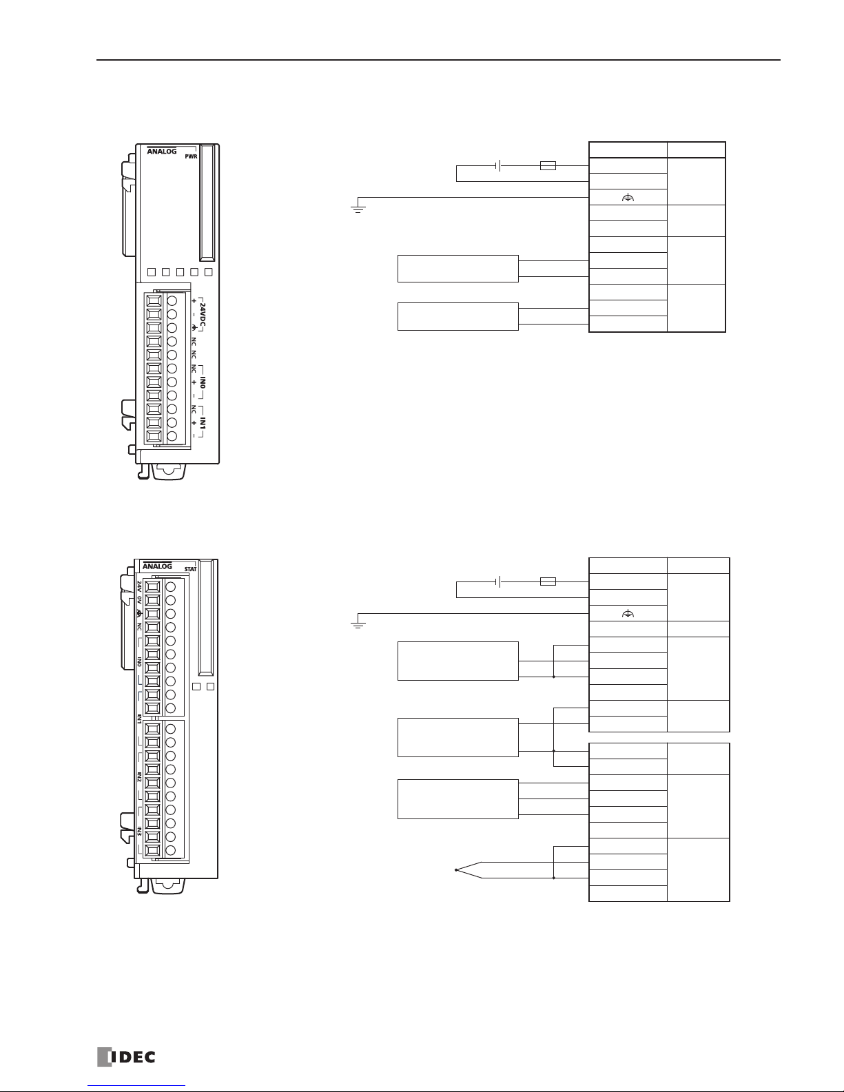
FC4A-J2A1 (Analog Input Module) — Screw Terminal Type
Applicable Terminal Block: FC4A-PMT11P (supplied with the analog input module)
FC4A-J4CN1 (Analog Input Module) — Screw Terminal Type
Applicable Terminal Block: FC4A-PMT10P (supplied with the analog input module)
Terminal No. Channel
+
24V DC–
NC
—
NC
NC
IN0+
–
NC
IN1+
–
• Connect a fuse appropriate for the applied voltage and current draw, at the position shown in the
diagram. This is required when equipment containing the MicroSmar t is destined for Europe.
• Do not connect any wiring to unused terminals.
Fuse
+–
24V DC
+
–
+
–
Analog voltage/current
output device
Analog voltage/current
output device
T
erminal No. Channel
24V
24V DC0V
NC —
CS
IN0
+
–
I–
CS
IN1
+
–
IN1
I–
CS
IN2
+
–
I–
CS
IN3
+
–
I–
• Connect a fuse appropriate for the applied voltage and current draw, at the position shown in the diagram. This is
required when equipment containing the MicroSmar t is destined for Europe.
• When connecting a resistance thermometer, connect three wires B, B’, and A to the CS (current sense), +, and – termi-
nals of input channels IN0 through IN3, respectively.
• When connecting a thermocouple, connect the + wire to the + terminal and the – wire to the CS and – terminals.
• Do not connect the thermocouple to a hazardous voltage (60V DC or 42.4V peak or higher).
• Do not connect any wiring to unused terminals.
• – terminals of input channels IN0 through IN3 are interconnected.
Fuse
+–
24V DC
Analog voltage
output device
–
+
Resistance
thermometer
A
B
B’
Thermocouple
+
–
NC
–
+
NC
NC
Analog current
output device
Phone: 800.894.0412 - Web: www.clrwtr.com - Email: [email protected]
Page 16
2: MODULE SPECIFICATIONS
2-10
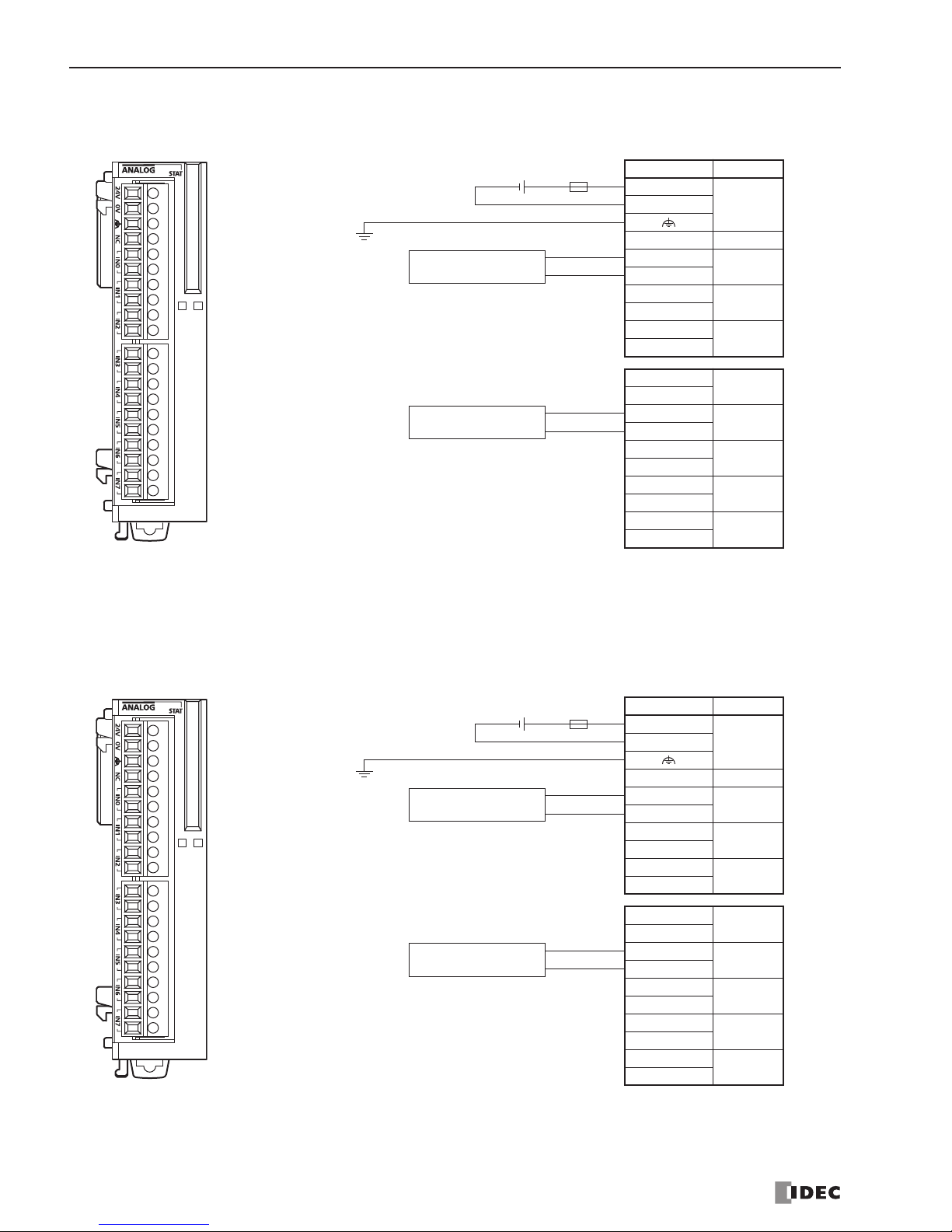
FC4A-J8C1 (Analog Input Module) — Screw Terminal Type
Applicable Terminal Block: FC4A-PMT10P (supplied with the analog input module)
FC4A-J8AT1 (Analog Input Module) — Screw Terminal Type
Applicable Terminal Block: FC4A-PMT10P (supplied with the analog input module)
T
erminal No. Channel
24V
24V DC0V
NC —
+
IN0
–
+
IN1
–
+
IN2
–
+
IN3
–
+
IN4
–
+
IN5
–
+
IN6
–
+
IN7
–
Fuse
+–
24V DC
Analog voltage
output device
–
+
Analog current
output device
–
+
• Connect a fuse appropriate for the applied voltage and
current draw, at the position shown in the diagram.
This is required when equipment containing the
MicroSmart is destined for Europe.
• Do not connect any wiring to unused terminals.
• – terminals of input channels IN0 through IN7 are
interconnected.
Terminal No. Channel
24V
24V DC0V
NC —
A
IN0
B
A
IN1
B
A
IN2
B
A
IN3
B
A
IN4
B
A
IN5
B
A
IN6
B
A
IN7
B
Fuse
+–
24V DC
NTC
Thermistor
B
A
PTC
Thermistor
B
A
• Connect a fuse appropriate for the applied voltage and
current draw, at the position shown in the diagram.
This is required when equipment containing the
MicroSmart is destined for Europe.
• Do not connect any wiring to unused terminals.
Phone: 800.894.0412 - Web: www.clrwtr.com - Email: [email protected]
Page 17
2: MODULE SPECIFICATIONS
2-11
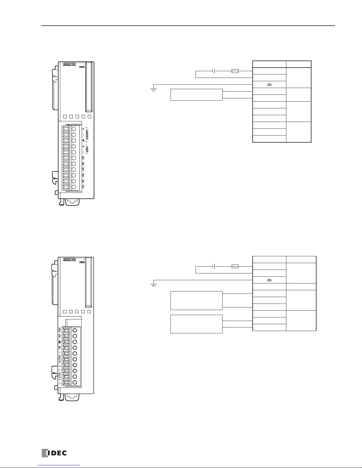
FC4A-K1A1 (Analog Output Module) — Screw Terminal Type
Applicable Terminal Block: FC4A-PMT11P (supplied with the analog output module)
FC4A-K2C1 (Analog Output Module) — Screw Terminal Type
Applicable Terminal Block: FC4A-PMT10P (supplied with the analog output module)
Terminal No. Channel
+
24V DC–
+
OUT
–
NC
—NC
NC
NC
—NC
NC
• Connect a fuse appropriate for the applied voltage and current draw, at the position shown in the
diagram. This is required when equipment containing the MicroSmar t is destined for Europe.
• Do not connect any wiring to unused terminals.
Fuse
+–
24V DC
+
–
Analog voltage/current
input device
Terminal No. Channel
24V
24V DC0V
NC —
V+
OUT0I+
–
V+
OUT1I+
–
Fuse
+–
24V DC
+
–
Analog voltage
input device
+
–
NC
NC
Analog current
input device
• Connect a fuse appropriate for the applied voltage and current draw, at the position shown in the
diagram. This is required when equipment containing the MicroSmar t is destined for Europe.
• Do not connect any wiring to unused terminals.
• – terminals of output channels OUT0 and OUT1 are interconnected.
Phone: 800.894.0412 - Web: www.clrwtr.com - Email: [email protected]
Page 18
2: MODULE SPECIFICATIONS
2-12
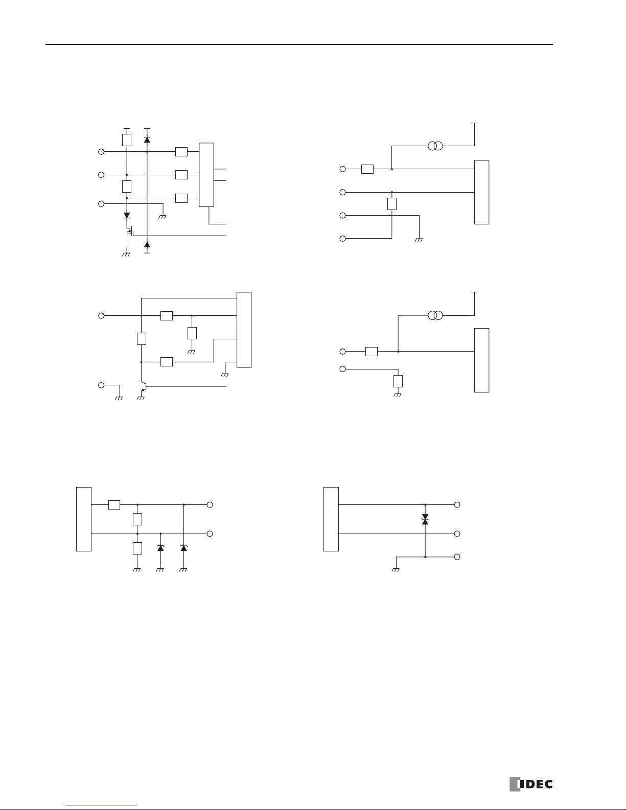
Type of Protection
Input Circuits
Output Circuits
1 k
Ω
NC (A)
Multiplexer
+ (B’)
FC4A-L03A1, FC4A-L03AP1, FC4A-J2A1
– (B)
1 kΩ
1 kΩ
+V2 +V1
–V1
10Ω
Input Data
Input
Selection
Signal
FC4A-J4CN1
15 MΩ
CS
Input Circuit
+
–
I–
15Ω
Current
Source
+
Input Circuit
–
FC4A-J8C1
10 kΩ
Input
Selection
Signal
100Ω
FC4A-J8AT1
A
Input Circuit
B
Current
Source
FC4A-L03A1, FC4A-L03AP1, FC4A-K1A1 FC4A-K2C1
Output Circuit
+
–
Output Circuit
V+
I+
–
Phone: 800.894.0412 - Web: www.clrwtr.com - Email: [email protected]
Page 19
2: MODULE SPECIFICATIONS
2-13
Power Supply for Analog I/O Modules
When supplying power to the analog I/O modules, take the following considerations.
• Power Supply for END Refresh Type Analog I/O Modules
Use separate power supplies for the MicroSmart CPU module and END refresh type analog I/O modules. Power up the
analog I/O modules at least 1 second earlier than the CPU module. This is recommended to ensure correct operation of the
analog I/O control.
• Power Supply for Ladder Refresh Type Analog I/O Modules
Use the same power supply for the MicroSmart CPU module and ladder refresh type analog I/O modules to suppress the
influence of noises.
After the CPU module has started to run, ladder refresh type analog input modules perform initialization for a maximum
of 5 seconds. During this period, the analog input data have an indefinite value. Design the user program to make sure that
the analog input data are read to the CPU module after the analog input operating status has changed to 0 (normal operation). For the analog input operating status, see page 4-13.
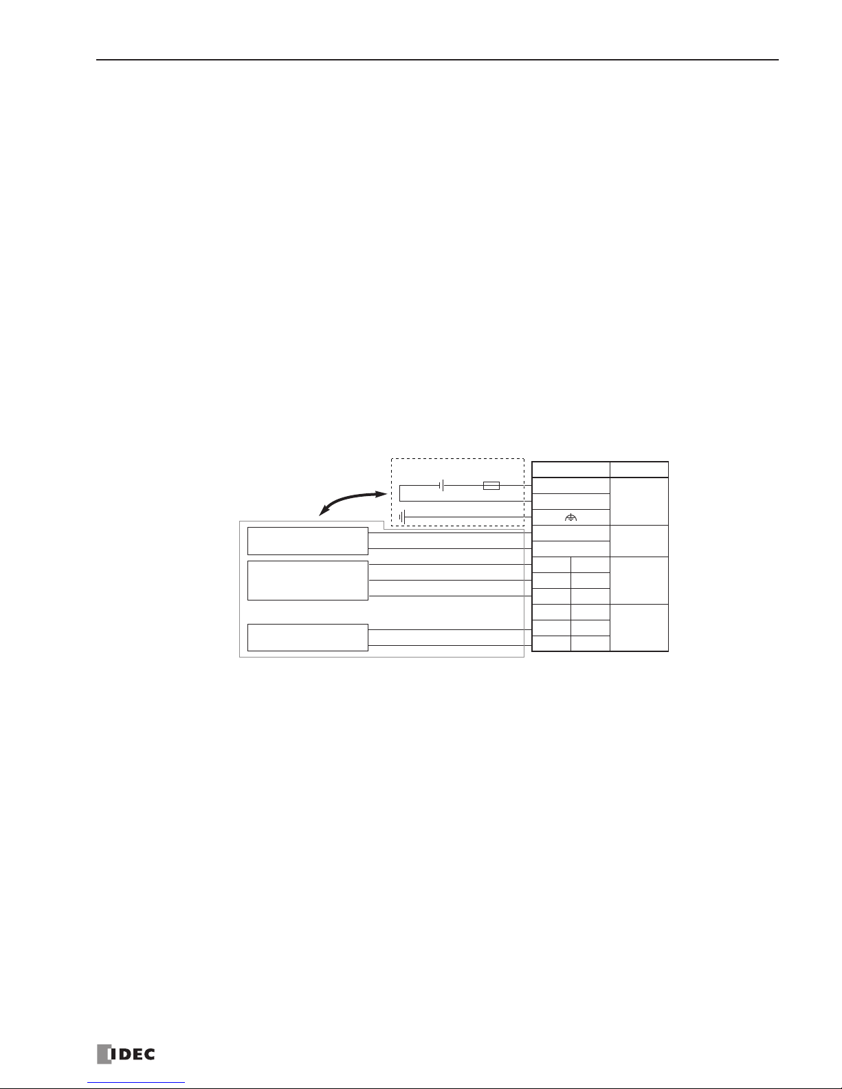
Wiring Analog I/O Lines
Separate the analog I/O lines, particularly resistance thermometer inputs, from motor lines as much as possible to suppress
the influence of noises.
T
erminal No. Channel
+
24V DC–
+
OUT
–
NC A
IN0+ B’
– B
NC A
IN1+ B’
– B
Fuse
+–
24V DC
Resistance
thermometer
B
+
–
A
B’
Analog voltage/current
input device
+
–
Analog voltage/current
output device
Separate the analog I/O line
from the power line.
Phone: 800.894.0412 - Web: www.clrwtr.com - Email: [email protected]
Page 20
2: MODULE SPECIFICATIONS
2-14
Dimensions
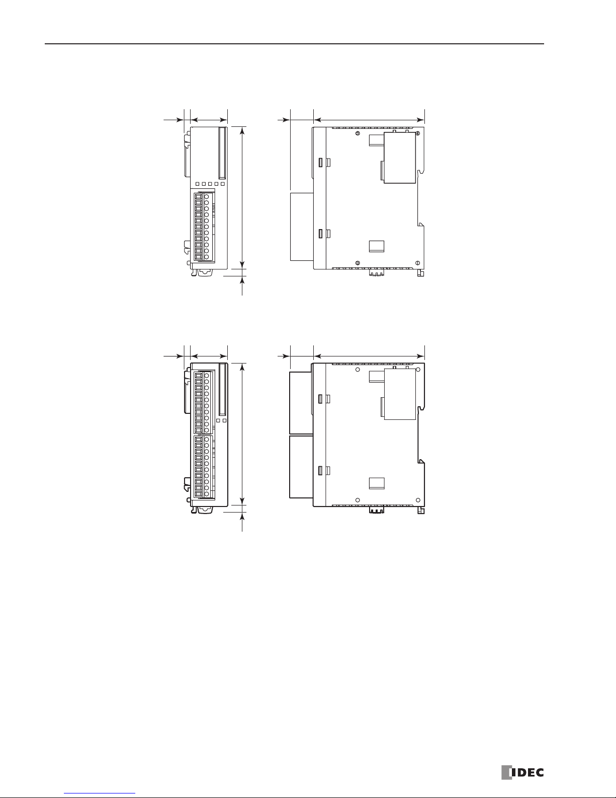
FC4A-L03A1, FC4A-L03AP1, FC4A-J2A1, FC4A-K1A1, FC4A-K2C1
FC4A-J4CN1, FC4A-J8C1, FC4A-J8AT1
23.5 14.6 70.0
90.04.5*
3.8
*8.5 mm when the clamp is pulled out.
All dimensions in mm.
23.5 14.6 70.0
90.04.5*
3.8
*8.5 mm when the clamp is pulled out.
Phone: 800.894.0412 - Web: www.clrwtr.com - Email: [email protected]
Page 21
3-1
3: INSTALLATION AND WIRING
Introduction
This chapter describes precautions for installing the analog I/O modules in connection with the internal current draw by
other expansion modules.
For general methods and precautions for installation and wiring of the analog I/O modules, see the FC4A MicroSmart
user’s manual (FC9Y-B812).
Mounting Hole Layout for Direct Mounting on Panel Surface
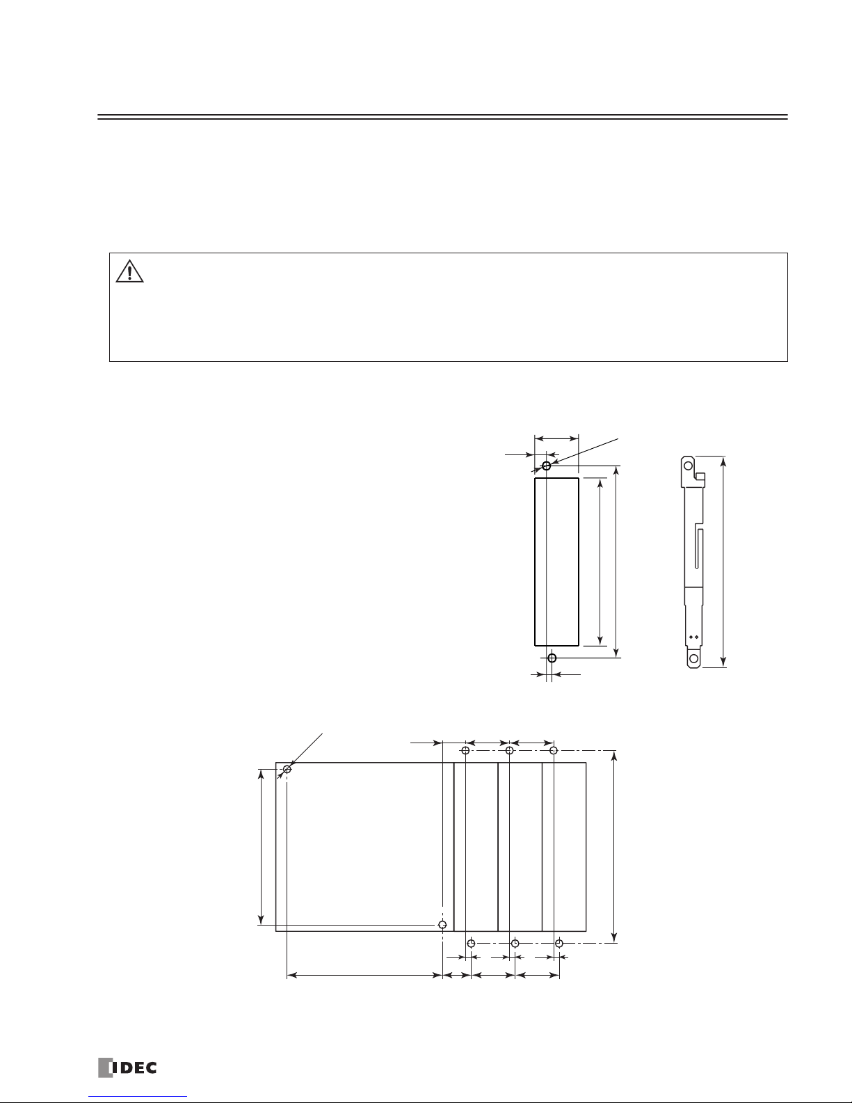
Example: Mounting hole layout for FC4A-C24R2 and three analog I/O modules
• This equipment is suitable for use in Class I, Division 2, Groups A, B, C, D or non-hazardous loca-
tions only.
• Explosion hazard — Substitution of components may impair suitability for Class I, Division 2.
• Explosion hazard — Do not disconnect equipment unless power has been switched off or the area is
known to be non-hazardous.
Warnin
g
103.0
90.0
2-ø4.3
6.3
23.5
3.0
113.0±0.2
Direct Mounting Strip
FC4A-PSP1P
To mount the analog I/O module on a panel surface, use
the direct mounting strip and two M4 screws (6 or 8 mm
long).
For details about the direct mounting strip, see the FC4A
MicroSmart user’s manual (FC9Y-B812).
All dimensions in mm.
3.0 3.0 3.0
23.583.0
83.0
10-ø4.3
103.0
15.3 23.5
12.3 23.5 23.5
Phone: 800.894.0412 - Web: www.clrwtr.com - Email: [email protected]
Page 22
3: INSTALLATION AND WIRING
3-2
Terminal Connection
Ferrules, Crimping Tool, and Screwdriver for Phoenix Terminal Blocks
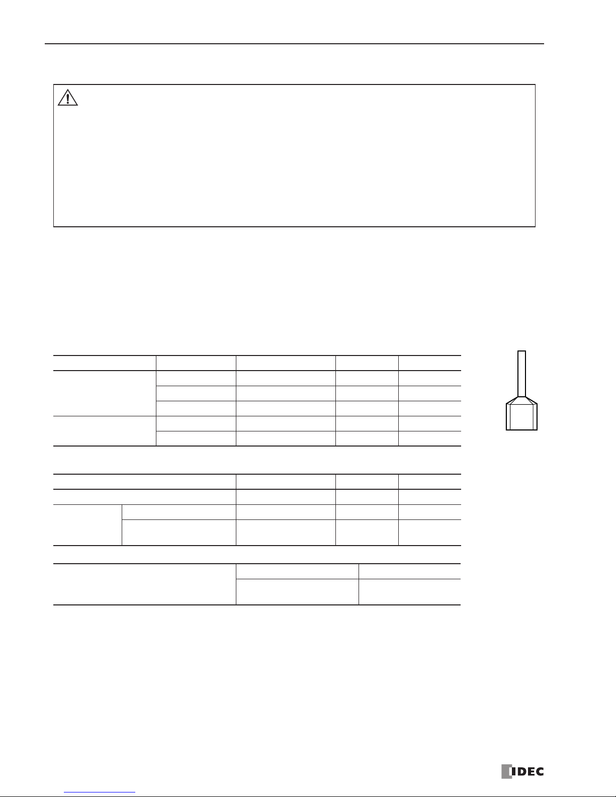
The screw terminal block can be wired with or without using ferrules on the end of cable. Applicable ferrules for the Phoenix terminal blocks and crimping tool for the ferrules are listed below. The screwdriver is used for tightening the screw terminals on the MicroSmart modules. These ferrules, crimping tool, and screwdriver are made by Phoenix Contact and are
available from Phoenix Contact.
Type numbers of the ferrules, crimping tool, and screwdriver listed below are the type numbers of Phoenix Contact. When
ordering these products from Phoenix Contact, specify the Order No. and quantity listed below.
Ferrule Order No.
Crimping Tool and Screwdriver Order No.
Quantity of Cables Cable Size Phoenix Type Order No. Pcs./Pkt.
For 1-cable connection
UL1007 AWG16 AI 1,5-8 BK 32 00 04 3 100
UL1007 AWG18 AI 1-8 RD 32 00 03 0 100
UL1015 AWG22 AI 0,5-8 WH 32 00 01 4 100
For 2-cable connection
UL1007 AWG18 AI-TWIN 2 x
0,75-8 GY 32 00 80 7 100
UL1015 AWG22 AI-TWIN 2 x 0,5-8 WH 32 00 93 3 100
Tool Name Phoenix Type Order No. Pcs./Pkt.
Crimping Tool
CRIMPFOX ZA 3 12 01 88 2 1
Screwdriver
For CPU modules SZS 0,6 x 3,5 12 05 05 3 10
For I/O modules and
communication adapter
SZS 0,4 x 2,5 12 05 03 7 10
Screw Terminal Tightening Torque
CPU modules 0.5 N·m
I/O modules
Communication adapter
0.22 to 0.25 N·m
Caution
• Make sure that the operating conditions and environments are within the specification values.
• Be sure to connect the grounding wire to a proper ground, otherwise electrical shocks may be
caused.
• Do not touch live terminals, otherwise electrical shocks may be caused.
• Do not touch terminals immediately after power is turned off, otherwise electrical shocks may be
caused.
• When using ferrules, insert a wire to the bottom of the ferrule and crimp the ferrule.
• When connecting a stranded wire or multiple solid wires to a screw terminal block, use a ferrule.
Otherwise the wire may slip off the screw terminal block.
Phone: 800.894.0412 - Web: www.clrwtr.com - Email: [email protected]
Page 23
4-1
4: ANALOG I/O CONTROL
Introduction
The MicroSmart provides analog I/O control capabilities of 12- through 16-bit resolution using analog I/O modules.
This chapter describes the system setup for using analog I/O modules, WindLDR programming procedures, data register
allocation numbers for analog I/O modules, and application examples.
For hardware specifications of analog I/O modules, see page 2-2.
System Setup
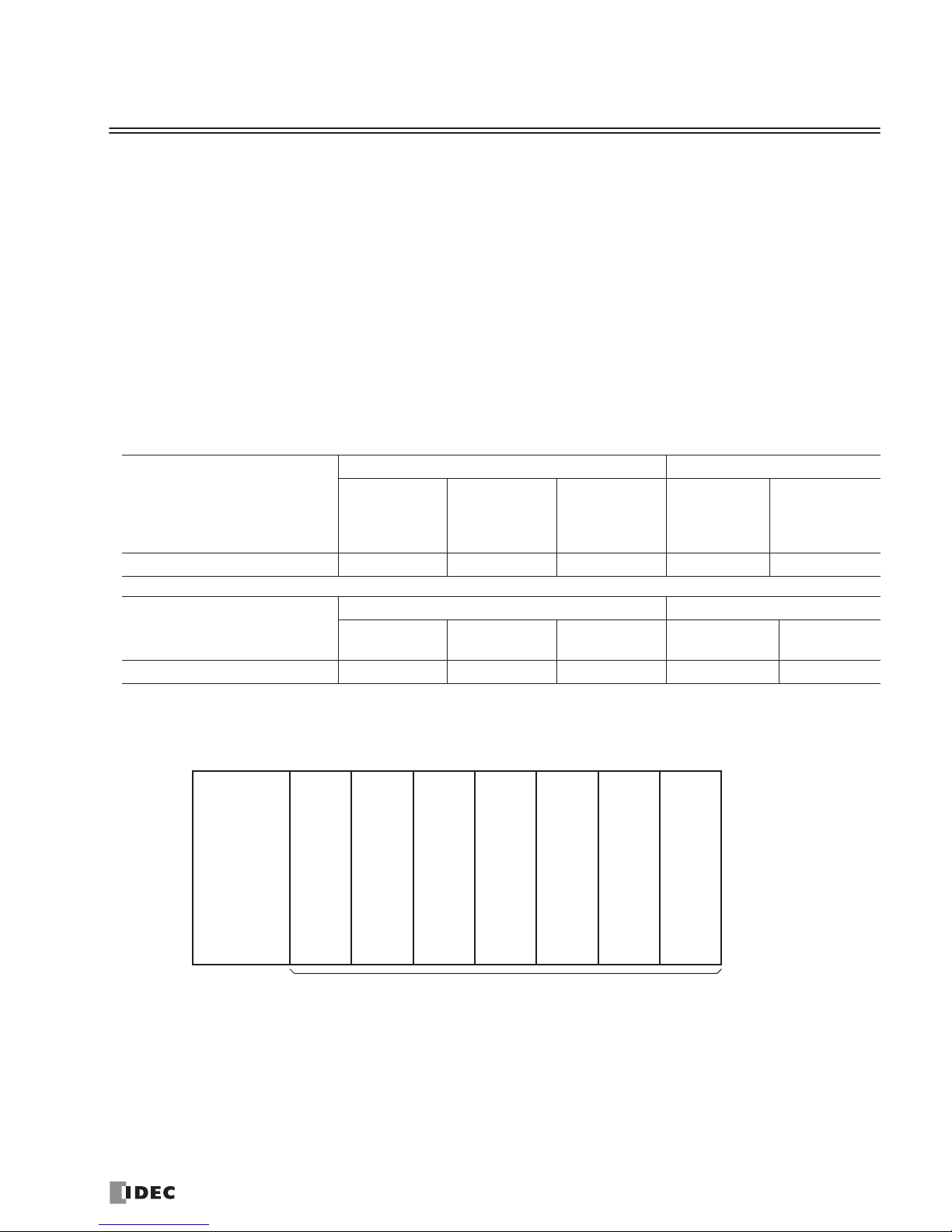
The FC4A and FC5A MicroSmart CPU modules can be used with a maximum of seven expansion I/O modules, which
include digital I/O modules and analog I/O modules.
Quantity of Applicable Analog I/O Modules
The quantity of the analog I/O modules that can be connected to the MicroSmart CPU module depends on the model of the
MicroSmart CPU modules as listed below:
System Setup Example
• Slot No.
Indicates the position where the expansion module is mounted. The slot number starts with 1 next to the CPU module up to
a maximum of 7.
Note: Analog I/O modules cannot be mounted to the right of the expansion interface module.
FC4A MicroSmart
CPU Module
All-in-One Type Slim Type
FC4A-C10R2
FC4A-C10R2C
FC4A-C16R2
FC4A-C16R2C
FC4A-C24R2
FC4A-C24R2C
FC4A-D20K3
FC4A-D20S3
FC4A-D20RK1
FC4A-D20RS1
FC4A-D40K3
FC4A-D40S3
Quantity of Analog I/O Modules — — 4 7 7
FC5A MicroSmart
CPU Module
All-in-One Type Slim Type
FC5A-C10R2
FC5A-C10R2C
FC5A-C16R2
FC5A-C16R2C
FC5A-C24R2
FC5A-C24R2C
FC5A-D16RK1
FC5A-D16RS1
FC5A-D32K3
FC5A-D32S3
Quantity of Analog I/O Modules — — 4 7 7
Analog
Slot No.:
1 2 3 4
I/O
Expansion I/O Modules (7 maximum)
Module
Slim Type
5 6 7
Digital
I/O
Module
Analog
I/O
Module
Analog
I/O
Module
Digital
I/O
Module
Digital
I/O
Module
Analog
I/O
Module
CPU Module
Phone: 800.894.0412 - Web: www.clrwtr.com - Email: [email protected]
Page 24
4: ANALOG I/O CONTROL
4-2
Programming WindLDR
Use WindLDR ver. 5.0 or later which has the ANST (Set Analog Module Parameters) macro for easy programming of analog I/O modules. For a start input of the ANST macro, use special internal relay M8120 (initialize pulse) to execute the
ANST macro only once after starting the CPU.
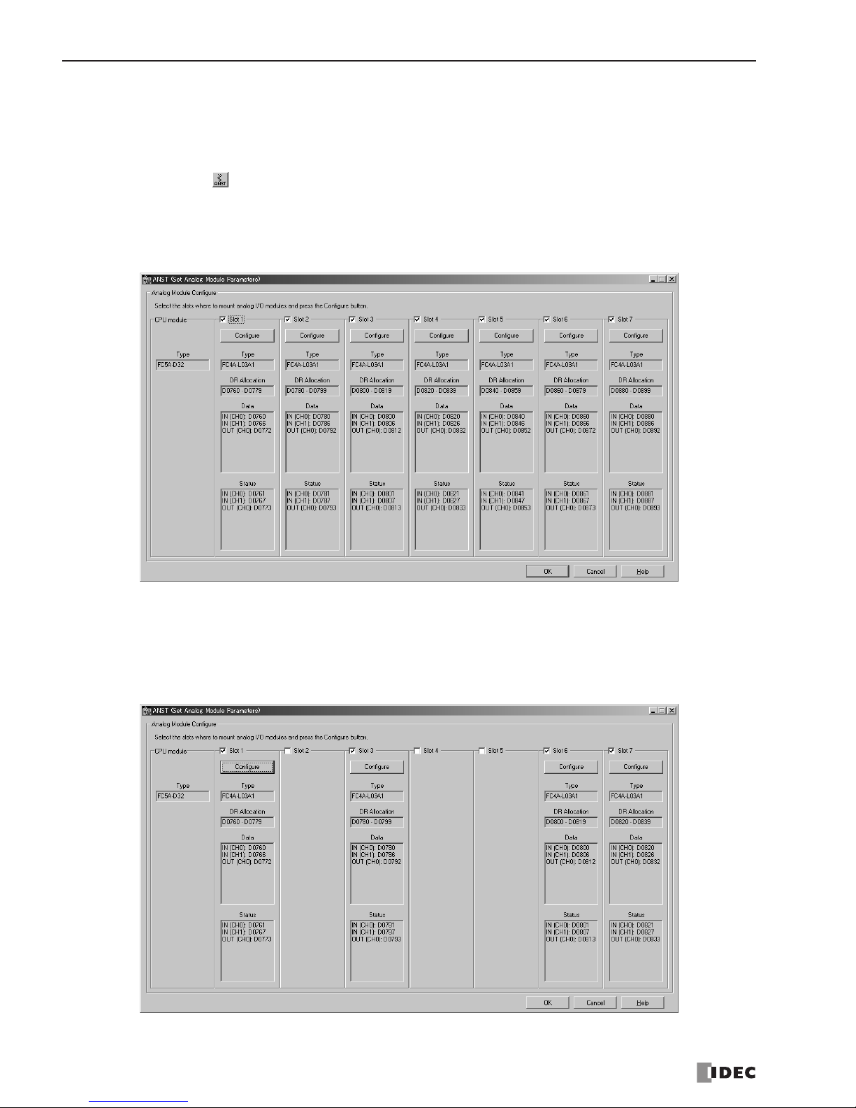
1. Click the ANST icon from the WindLDR tool bar, then place the cursor where you want to insert the ANST
instruction on the ladder editing screen, and click the mouse.
Or, place the cursor where you want to insert the ANST instruction on the ladder editing screen, and type
ANST.
The Set Analog Module Parameters dialog box appears.
2. Select the slots where analog I/O modules are mounted.
All slots are selected to use seven analog I/O modules as default. Click the check box to deselect slots where analog I/O
modules are not mounted.
When using analog I/O modules on Slots 1, 3, 6, and 7, deselect Slots 2, 4, and 5 as shown below.
Phone: 800.894.0412 - Web: www.clrwtr.com - Email: [email protected]
Page 25
4: ANALOG I/O CONTROL
4-3
3. Click the Configure button under the selected slots.
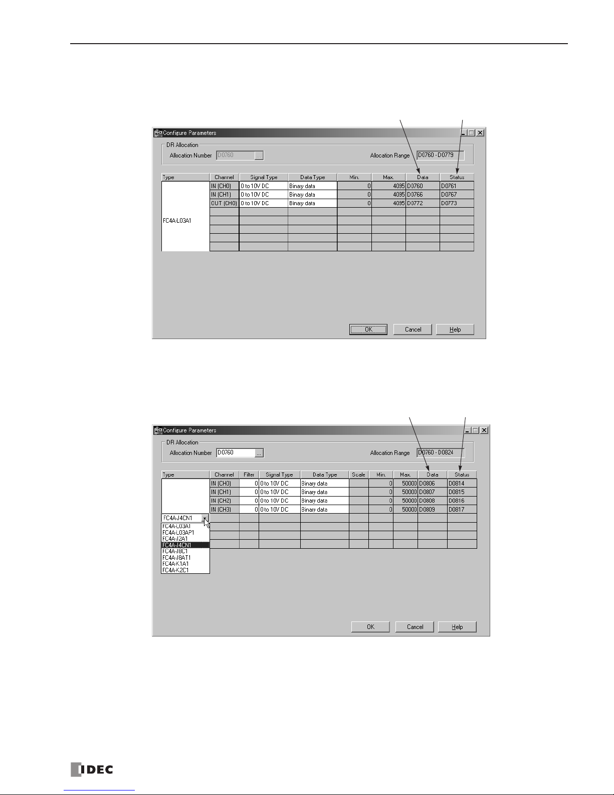
The Configure Parameters dialog box appears. All parameters for analog I/O control can be set in this dialog box. Available parameters vary with the type of the analog I/O module.
4. Select the type of the analog I/O module.
Click on the right of the analog I/O module Type No., then a pull-down list shows eight available modules.
Depending on the selected analog I/O module, other parameters available for the selected module are shown.
In the Configure Parameters dialog box, parameters in white cells are selectable while gray cells indicate default parameters. In the white cells, optional values can be selected from a pull-down list or entered by typing required values.
Note for PID Instruction Source Operand S4 (process variable)
When using the PID instruction, specify the data register number shown under Data in the Configure Parameters dialog box
as source operand S4 (process variable) of the PID instruction. The analog input data in the selected data register is used
as the process variable of the PID instruction.
END Refresh Type Configure Parameters dialog box
FC4A-L03A1
FC4A-L03AP1
FC4A-J2A1
FC4A-K1A1
Analog I/O Data (Note) Analog I/O Operating Status
Ladder Refresh Type Configure Parameters dialog box
FC4A-J4CN1
FC4A-J8C1
FC4A-J8AT1
FC4A-K2C1
Analog I/O Data (Note) Analog I/O Operating Status
Phone: 800.894.0412 - Web: www.clrwtr.com - Email: [email protected]
Page 26
4: ANALOG I/O CONTROL
4-4
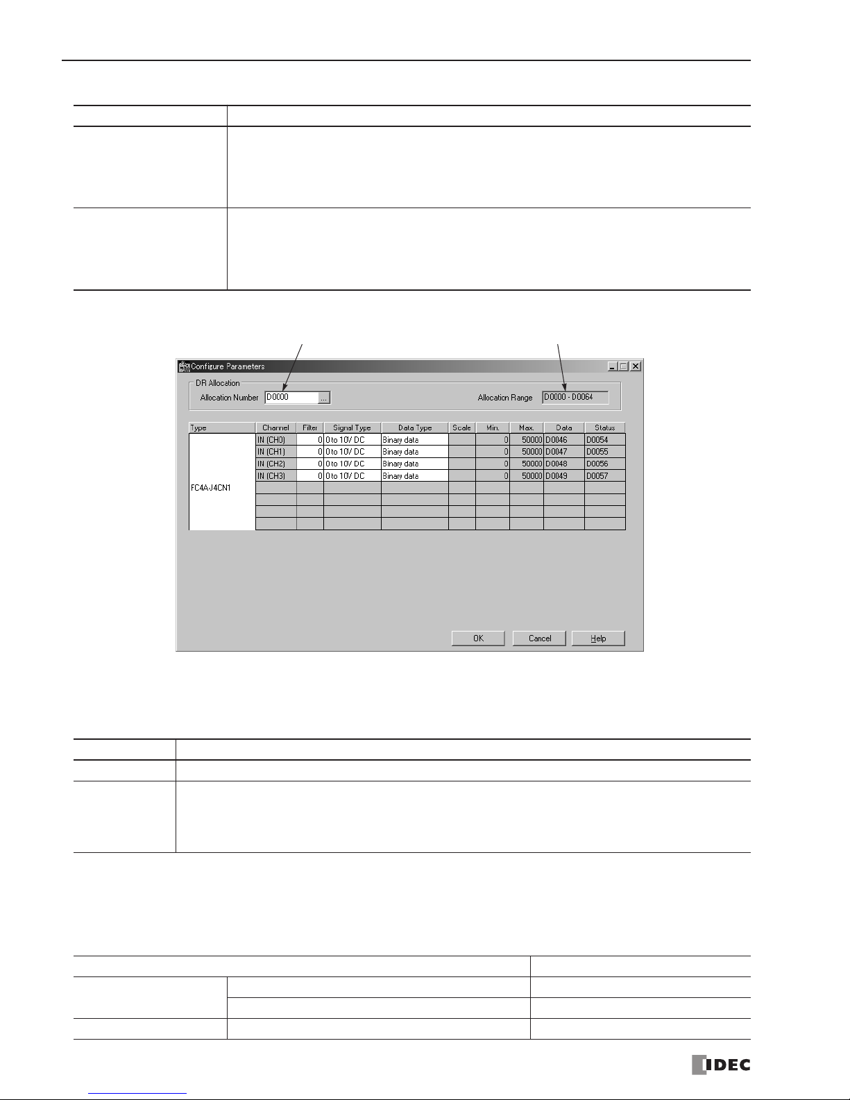
5. Select a DR allocation number (Ladder refresh type only).
6. Enter a filter value (Ladder refresh type analog input modules only).
The filter function is available for the FC4A-J4CN1, FC4A-J8C1, and FC4A-J8AT1 only. Filtering ensures smooth input
of analog data into the CPU module.
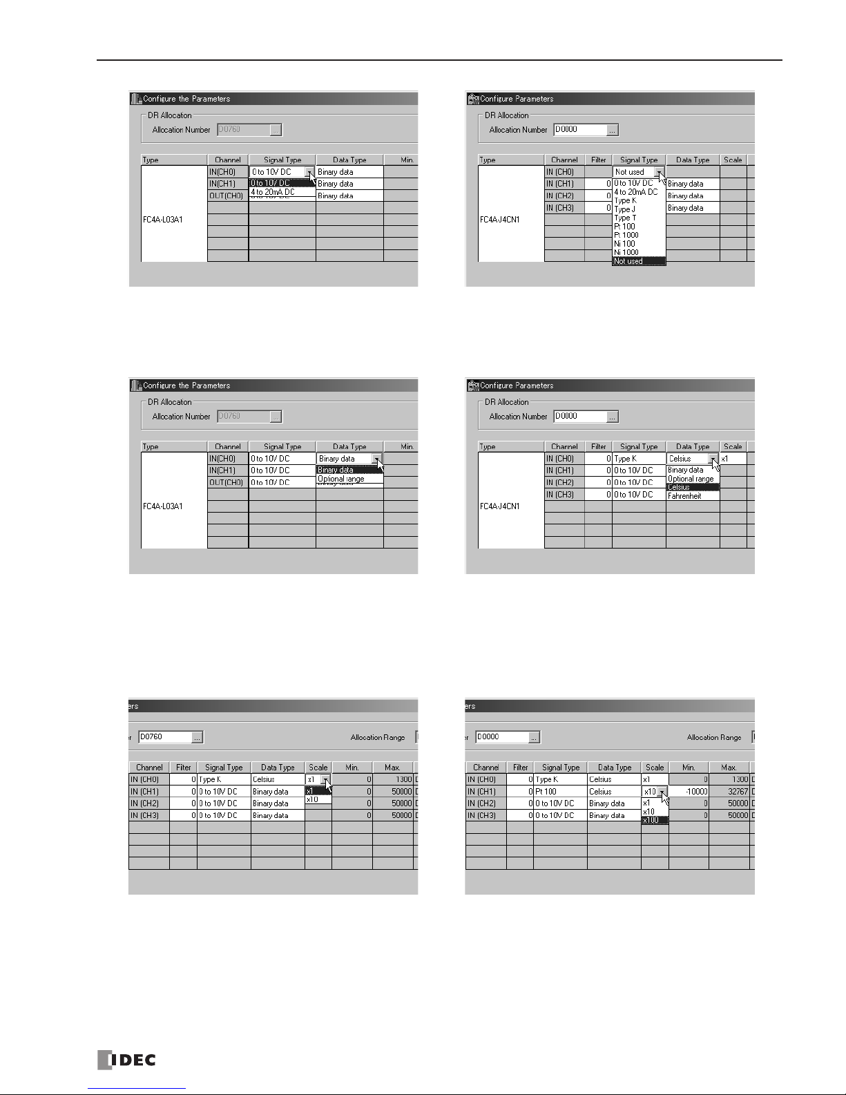
7. Select a signal type for each channel.
Click on the right of the Signal Type field, then a pull-down list appears to show all available input or output signal types.
When you do not use any input or output signal, select the default value or Not used for the channel.
CPU Module DR Allocation
END Refresh Type
FC4A-L03A1
FC4A-L03AP1
FC4A-J2A1
FC4A-K1A1
DR allocation starts with D760 as default, and the first DR number cannot be changed.
One analog I/O module occupies 20 data registers. When a maximum of seven analog I/O
modules ar
e used, data registers D760 through D899 are used for analog I/O contr
ol.
Ladder Refresh Type
FC4A-J4CN1
FC4A-J8C1
FC4A-J8AT1
FC4A-K2C1
The first data register can be selected as required. Enter the first DR number used for analog
I/O contr
ol.
One analog input module occupies a maximum of 65 data registers.
One analog output module occupies 15 data registers.
Filter Value Description
0 or 1 Without filter function
2 to 255
The average of N pieces of analog input data is read as analog input data, where N is the designated
filter value.
Analog I/O Module For unused channel, select
END Refresh Type
FC4A-L03A1, FC4A-J2A1 0 to 10V DC
FC4A-L03AP1 Type K
Ladder Refresh Type FC4A-J4CN1, FC4A-J8C1, FC4A-J8AT1, FC4A-K2C1
Not used
Ladder Refr
esh Type Configure Parameters dialog box
First Data Register No. Allocation range changes automatically.
Analog input data
(Previous analog input data) (Filter value) (Current analog input data)+×
(Filter value) 1+
--------------------------------------------------------------------------------------------------------------------------------------------------------------------------------------------=
Phone: 800.894.0412 - Web: www.clrwtr.com - Email: [email protected]
Page 27
4: ANALOG I/O CONTROL
4-5
8. Select a data type for each channel.
Click on the right of the Data Type field, then a pull-down list appears to show all available input or output data types.
9. Select a scale value (Ladder refresh type analog input modules only).
When Celsius or Fahrenheit is selected for thermocouple, resistance thermometer, or thermistor signal types on ladder
refresh type analog input modules, the scale value can be selected from ×1, ×10, or ×100 depending on the selected signal
type. Using this function, the analog input data can be multiplied to ensure precise control.
Phone: 800.894.0412 - Web: www.clrwtr.com - Email: [email protected]
Page 28
4: ANALOG I/O CONTROL
4-6
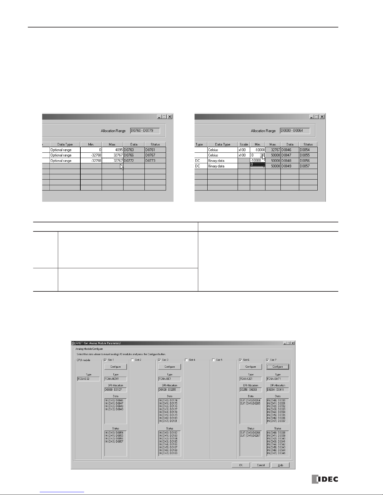
10. Select maximum and minimum values.
For analog input values, when Optional range is selected for the Data Type, designate the analog input data minimum and
maximum values which can be –32,768 through 32,767.
In addition, when using resistance thermometers (Pt100, Pt1000, Ni100, or Ni1000) with the Celsius or Fahrenheit Data
Type and the ×100 scale, select the analog input data minimum value from 0 or another value in the pull-down list. The
maximum value is changed automatically according to the selected minimum value.
For analog output values, when Optional range is selected for the Data Type, designate the analog output data minimum
and maximum values which can be –32,768 through 32,767.
11. View the data register numbers allocated to Data and Status.
12. Click the OK button to save changes and exit the Configure Parameter dialog box.
13. Repeat the same steps for other slots.
14. When finished, click the OK button to save changes and exit the Set Analog Module Parameters dialog box.
Parameter DR Allocation
Data
Analog I/O Data
Stores the digital data converted from an analog input
signal or converted into an analog output signal.
Designated as source operand S4 (process variable)
of the PID instruction.
END Refresh Type
Data registers are automatically allocated depending
on the slot where the analog I/O module is mounted.
Ladder Refresh Type
Data registers are automatically allocated depending
on the number designated in the DR Allocation Number field.
Status
Analog I/O Operating Status
Stores an analog I/O operating status code.
See pages 4-13 and 4-15
.
Phone: 800.894.0412 - Web: www.clrwtr.com - Email: [email protected]
Page 29

4: ANALOG I/O CONTROL
4-7
Analog I/O Control Parameters
Available parameters for analog I/O control depend on the type of analog I/O modules as summarized in the following
table. Designate the parameters in the Configure Parameters dialog box of the ANST macro as required by your application.
Parameter
Analog I/O Module Analog Input Module Analog Output Module
END Refresh Type Ladder Refresh Type END Ladder
FC4A-
L03A1
FC4A-
L03AP1
FC4A-
J2A1
FC4A-
J4CN1
FC4A-
J8C1
FC4A-
J8AT1
FC4A-
K1A1
FC4A-
K2C1
Analog Input Signal Type
X X X X X X — —
Page 4-11 Page 4-11 —
Analog Input Data Type
X X X X X X — —
Page 4-11 Page 4-11 —
Analog Input Data
Minimum/Maximum Values
X X X X X X — —
Page 4-13 Page 4-13 —
Filter Value
— — — X X X — —
— — Page 4-13 —
Thermistor Parameter
— — — — — X — —
— — 4-13 —
Analog Input Data
X X X X X X — —
Page 4-13 Page 4-13 —
Analog Input
Operating Status
X X X X X X — —
Page 4-13 Page 4-13 —
Analog Output Signal Type
X X — — — — X X
Page 4-15 — Page 4-15
Analog Output Data Type
X X — — — — X X
Page 4-15 — Page 4-15
Analog Output Data
Minimum/Maximum Values
X X — — — — X X
Page 4-15 — Page 4-15
Analog Output Data
X X — — — — X X
Page 4-15 — Page 4-15
Analog Output
Operating Status
X
X — — — — X X
Page 4-15 — Page 4-15
Phone: 800.894.0412 - Web: www.clrwtr.com - Email: [email protected]
Page 30

4: ANALOG I/O CONTROL
4-8
Data Register Allocation Numbers for Analog I/O Modules
Analog I/O modules are numbered from 1 through 7, in the order of increasing distance from the CPU module. Data registers are allocated to each analog I/O module depending on the analog I/O module number. END refresh type analog I/O
modules and ladder refresh type analog I/O modules have different data register allocation.
END Refresh Type Analog I/O Modules
Each END refresh type analog I/O module is automatically allocated 20 data registers to store parameters for controlling
analog I/O operation, starting with D760 through D779 for analog I/O module No. 1, up to D880 through D899 for analog
I/O module No. 7. When a maximum of seven analog I/O modules are not used, data registers allocated to the unused analog I/O module numbers can be used as ordinary data registers.
When a maximum of seven END refresh type analog I/O modules are mounted, data registers D760 through D899 are
allocated to analog modules 1 through 7 as shown below. The ANST macro is used to program data registers for the analog
I/O module configuration. The CPU module checks the analog I/O configuration only once when the CPU starts to run. If
you have changed the parameter while the CPU is running, stop and restart the CPU to enable the new parameter.
The END refresh type analog I/O module number starts with 1 next to the CPU module up to a maximum of 7.
The run-time program download and test program download cannot be used to change analog I/O parameters.
Note: Data registers allocated to the unused analog I/O module numbers can be used as ordinar y data registers.
Channel Function
END Refresh Type Analog I/O Module No.
R/W
1 2 3 4 5 6 7
Analog
Input
Ch 0
Analog input data D760 D780 D800 D820 D840 D860 D880 R
Analog input operating status D761 D781 D801 D821 D841 D861 D881 R
Analog input signal type D762 D782 D802 D822 D842 D862 D882 R/W
Analog input data type D763 D783 D803 D823 D843 D863 D883 R/W
Analog input data minimum value D764 D784 D804 D824 D844 D864 D884 R/W
Analog input data maximum value D765 D785 D805 D825 D845 D865 D885 R/W
Analog
Input
Ch 1
Analog input data D766 D786 D806 D826 D846 D866 D886 R
Analog input operating status D767 D787 D807 D827 D847 D867 D887 R
Analog input signal type D768 D788 D808 D828 D848 D868 D888 R/W
Analog input data type D769 D789 D809 D829 D849 D869 D889 R/W
Analog input data minimum value D770 D790 D810 D830 D850 D870 D890 R/W
Analog input data maximum value D771 D791 D811 D831 D851 D871 D891 R/W
Analog
Output
Analog output data D772 D792 D812 D832 D852 D872 D892 R/W
Analog output operating status D773 D793 D813 D833 D853 D873 D893 R
Analog output signal type D774 D794
D814 D834 D854 D874 D894 R/W
Analog output data type D775 D795 D815 D835 D855 D875 D895 R/W
Analog output data minimum value D776 D796 D816 D836 D856 D876 D896 R/W
Analog output data maximum value D777 D797 D817 D837 D857 D877 D897 R/W
– Reserved –
D778 D798 D818 D838 D858 D878 D898 R/W
D779 D799 D819 D839 D859 D879 D899
R/W
Phone: 800.894.0412 - Web: www.clrwtr.com - Email: [email protected]
Page 31
4: ANALOG I/O CONTROL
4-9
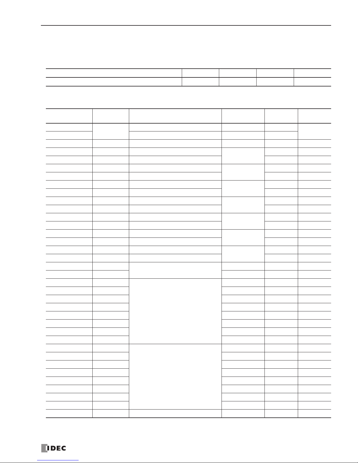
Ladder Refresh Type Analog I/O Modules
When using a ladder refresh type analog input or output module, the first data register number can be designated in the
ASNT macro dialog box. The quantity of required data registers depends on the model of the ladder refresh type analog
input or output module.
Data register numbers and parameters are shown in the table below.
Ladder Refresh Type Analog Input Module Data Register Allocation (FC4A-J4CN1, FC4A-J8C1, and FC4A-J8AT1)
* Data registers for channels 4 through 7 are reser ved on the FC4A-J4CN1.
Analog I/O Module FC4A-J4CN1 FC4A-J8C1 FC4A-J8AT1 FC4A-K2C1
Quantity of Data Registers for Analog I/O Operation
65 65 65 15
Data Register
Number Offset
Data Size
(word)
Parameter Channel Default R/W
+0 (Low Byte)
1
Analog input signal type CH0 FFh
R/W
+0 (High Byte) — Reserved — All channels 00h
+1 4 Analog input data configuration CH0 0 R/W
+5 1 Analog input signal type
CH1
00FFh R/W
+6 4 Analog input data configuration 0 R/W
+10 1 Analog input signal type
CH2
00FFh R/W
+11 4 Analog input data configuration 0 R/W
+15 1 Analog input signal type
CH3
00FFh R/W
+16 4 Analog input data configuration 0 R/W
+20 1 Analog input signal type
CH4 *
00FFh R/W
+21 4 Analog input data configuration 0 R/W
+25 1 Analog input signal type
CH5 *
00FFh R/W
+26 4 Analog input data configuration 0 R/W
+30 1 Analog input signal type
CH6 *
00FFh R/W
+31 4 Analog input data configuration 0 R/W
+35 1 Analog input signal type
CH7 *
00FFh R/W
+36 4 Analog input data configuration 0 R/W
+40 3
Thermistor parameters
(FC4A-J8AT1 only)
CH0 to CH3 0 R/W
+43 3 CH4 to CH7 * 0 R/W
+46 1
Analog input data
CH0 — R
+47 1 CH1 — R
+48 1 CH2 — R
+49 1 CH3 — R
+50 1 CH4 * — R
+51 1 CH5 * — R
+52 1 CH6 * — R
+53 1 CH7 * — R
+54 1
Analog input operating status
CH0 — R
+55 1 CH1 — R
+56 1 CH2 — R
+57 1 CH3 — R
+58 1 CH4 * — R
+59 1 CH5 * — R
+60 1 CH6 * — R
+61 1 CH7 * — R
+62 3 — Reserved — All channels —
R
Phone: 800.894.0412 - Web: www.clrwtr.com - Email: [email protected]
Page 32
4: ANALOG I/O CONTROL
4-10
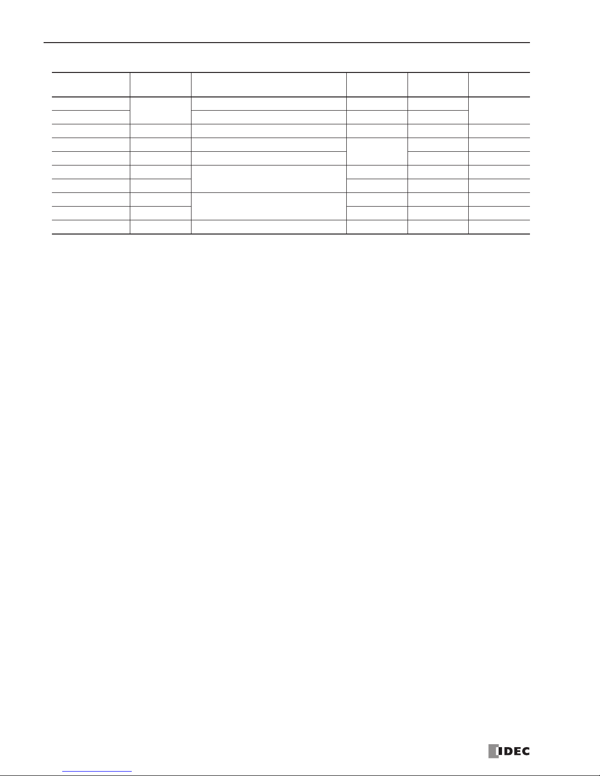
Ladder Refresh Type Analog Output Module Data Register Allocation (FC4A-K2C1)
Data Register
Number Offset
Data Size
(word)
Parameter Channel Default R/W
+0 (Low Byte)
1
Analog output signal type CH0 FFh
R/W
+0 (High Byte) — Reserved — All channels 00h
+1 3 Analog output data configuration CH0 0 R/W
+4 1 Analog output signal type
CH1
00FFh R/W
+5 3 Analog output data configuration 0 R/W
+8 1
Analog output data
CH0 0 R/W
+9 1 CH1 0 R/W
+10 1
Analog output operating status
CH0 — R
+11 1 CH1 — R
+12 3 — Reserved — All channels —
R
Phone: 800.894.0412 - Web: www.clrwtr.com - Email: [email protected]
Page 33
4: ANALOG I/O CONTROL
4-11
Analog Input Parameters
Analog input parameters include the analog input signal type, analog input data type, analog input minimum and maximum values, filter value, thermistor parameter, analog input data, and analog input operating status. This section describes
these parameters in detail.
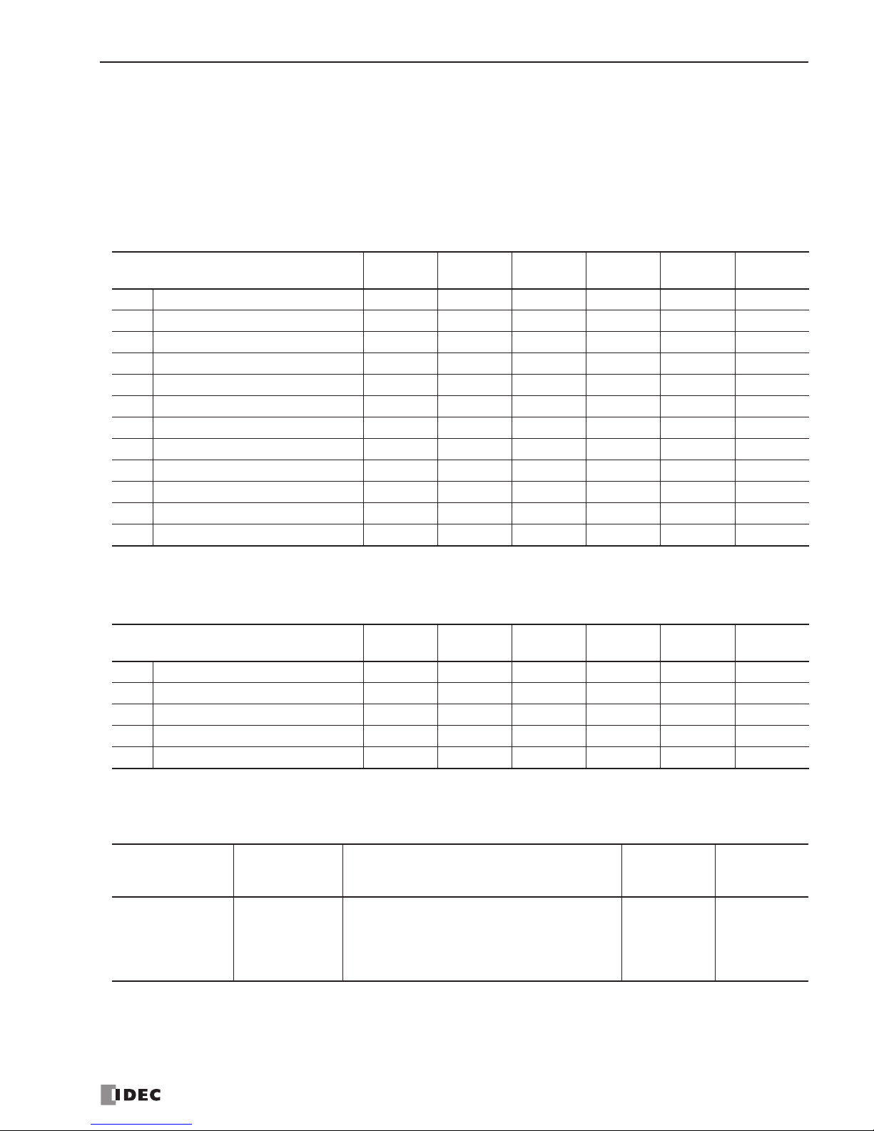
Analog Input Signal Type
A total of 11 analog input signal types are available, depending on the analog I/O or analog input module. Select an analog
input signal type for each analog input channel. When a channel is not used, select the default value or Not used for the
channel.
Analog Input Data Type
A total of five analog input data types are available, depending on the analog I/O or analog input module. Select an analog
input data type for each analog input channel.
Binary Data
When Binary data is selected as an analog input data type, the analog input is linearly converted into digital data in the
range described in the table below.
Parameter
FC4A-
L03A1
FC4A-
L03AP1
FC4A-
J2A1
FC4A-
J4CN1
FC4A-
J8C1
FC4A-
J8AT1
0 Voltage input (0 to 10V DC) X — X X X —
1 Current input (4 to 20 mA DC) X — X X X —
2 Type K thermocouple — X — X — —
3 Type J thermocouple — X — X — —
4 Type T thermocouple — X — X — —
5 Pt 100 resistance thermometer — X — X — —
6 Pt 1000 resistance thermometer — — — X — —
7 Ni 100 resistance thermometer — — — X — —
8 Ni 1000 resistance thermometer — — — X — —
9 NTC type thermistor — — — — — X
10 PTC type thermistor — — — — — X
255 Not used — — — X X X
Parameter
FC4A-
L03A1
FC4A-
L03AP1
FC4A-
J2A1
FC4A-
J4CN1
FC4A-
J8C1
FC4A-
J8AT1
0 Binar y data X X X X X X
1 Optional range X X X X X X
2 Celsius — X — X — NTC only
3 Fahrenheit — X — X — NTC only
4 Resistance — — — — — X
Type No.
FC4A-L03A1
FC4A-L03AP1
FC4A-J2A1
FC4A-J4CN1 FC4A-J8C1 FC4A-J8AT1
Analog Input Data 0 to 4095
Analog Input Signal Type Analog Input Data
Voltage/Current: 0 to 50,000
Thermocouple: 0 to 50,000
Pt100, Ni100: 0 to 6,000
Pt1000, Ni1000: 0 to 60,000
0 to 50000
0 to 4000
Phone: 800.894.0412 - Web: www.clrwtr.com - Email: [email protected]
Page 34
4: ANALOG I/O CONTROL
4-12
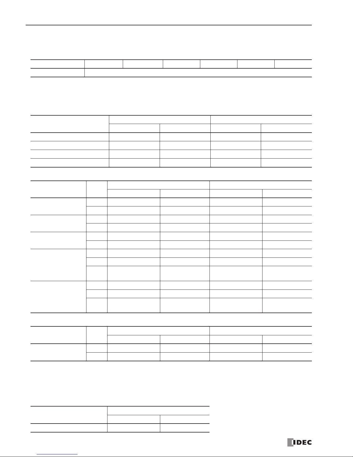
Optional Range
When Optional range is selected as an analog input data type, the analog input is linearly converted into digital data in the
range between the minimum and maximum values designated in the Configure Parameters dialog box.
Celsius and Fahrenheit
When Celsius or Fahrenheit is selected as an analog input data type, the analog input data range depends on the analog
input signal type, scale value, and the type of the analog input module, FC4A-L03AP1, FC4A-J4CN1, and FC4A-J8AT1.
• FC4A-L03AP1
• FC4A-J4CN1
• FC4A-J8AT1
Resistance
When Resistance is selected as an analog input data type, the analog input is linearly converted into digital data in the
range described in the table below. This option is available only when NTC or PTC type thermistor is selected for the
FC4A-J8AT1.
• FC4A-J8AT1
Type No. FC4A-L03A1 FC4A-L03AP1 FC4A-J2A1 FC4A-J4CN1 FC4A-J8C1 FC4A-J8AT1
Analog Input Data Analog input data minimum value to maximum value (–32768 to 32767)
Analog Input Signal Type
Celsius Fahrenheit
Temperature (°C) Analog Input Data Temperature (°F) Analog Input Data
Type K thermocouple 0 to 1300 0 to 13000 32 to 2372 320 to 23720
Type J thermocouple 0 to 1200 0 to 12000 32 to 2192 320 to 21920
Type T thermocouple 0 to 400 0 to 4000 32 to 752 320 to 7520
Pt100 resistance thermometer –100.0 to 500.0 –1000 to 5000 –148.0 to 932.0 –1480 to 9320
Analog Input
Signal Type
Scale
Celsius Fahrenheit
Temperature (°C) Analog Input Data Temperature (°F) Analog Input Data
Type K thermocouple
×1 0 to 1300 0 to 1300 32 to 2372 32 to 2372
×10 0.0 to 1300.0 0 to 13000 32.0 to 2372.0 320 to 23720
Type J thermocouple
×1 0 to 1200 0 to 1200 32 to 2192 32 to 2192
×10 0.0 to 1200.0 0 to 12000 32.0 to 2192.0 320 to 21920
Type T thermocouple
×1 0 to 400 0 to 400 32 to 752 32 to 752
×10 0.0 to 400.0 0 to 4000 32.0 to 752.0 320 to 7520
Pt100, Pt1000
resistance
thermometer
×1 –100 to 500 –100 to 500 –148 to 932 –148 to 932
×10 –100.0 to 500.0 –1000 to 5000 –148.0 to 932.0 –1480 to 9320
×100
0.00 to 500.00
–100.00 to 327.67
0 to 50000
–10000 to 32767
0.00 to 655.35
–148.00 to 327.67
0 to 65535
–14800 to 32767
Ni100, Ni1000
resistance
thermometer
×1 –60 to 180 –60 to 180 –76 to 356 –76 to 356
×10 –60.0 to 180.0 –600 to 1800 –76.0 to 356.0 –760 to 3560
×100 –60.00 to 180.00 –6000 to 18000
0.00 to 356.00
–76.00 to 327.67
0 to 35600
–7600 to 32767
Analog Input
Signal Type
Scale
Celsius Fahrenheit
Temperature (°C) Analog Input Data Temperature (°F) Analog Input Data
NTC thermistor
×1 –50 to 150 –50 to 150 –58 to 302 –58 to 302
×10 –50.0 to 150.0 –500 to 1500 –58.0 to 302.0 –580 to 3020
Analog Input Signal Type
Resistance
Resistance (Ω) Analog Input Data
NTC/PTC thermistor 0 to 100000 0 to 10000
Phone: 800.894.0412 - Web: www.clrwtr.com - Email: [email protected]
Page 35

4: ANALOG I/O CONTROL
4-13
Analog Input Minimum/Maximum Values
For analog input values, when Optional range is selected for the Data Type, designate the analog input data minimum and
maximum values which can be –32,768 through 32,767.
In addition, when using resistance thermometers (Pt100, Pt1000, Ni100, or Ni1000) with the Celsius or Fahrenheit Data
Type and the ×100 scale, select the analog input data minimum value from 0 or another value in the pull-down list. The
maximum value is changed automatically according to the selected minimum value.
Filter Value
The filter function is available for the ladder input type FC4A-J4CN1, FC4A-J8C1, and FC4A-J8AT1 only. Filtering
ensures smooth input of analog data into the CPU module. For the filtering function of analog input signals, see page 4-4.
Valid values are 0 through 255.
Thermistor Parameter
Thermistor parameters are enabled when selecting NTC thermistor for the analog input type of the FC4A-J8AT1. The
same parameters are specified for four channels: CH0 to CH3 and CH4 to CH7.
For NTC type thermistors, analog input data can be calculated from the following formula:
For PTC type thermistors, linearize the analog input data using the XYFS instruction.
Analog Input Data
The analog input signal is converted into a digital value within the range specified by the analog input data type and applicable parameters, and is stored to a data register allocated to analog input data. The analog input data register number is
shown under Data in the Configure Parameters dialog box.
END Refresh Type
The analog input signal is converted into a digital value and stored to a data register, such as D760 or D766, allocated to
analog input channel 1 or 2 on analog module number 1 through 7 depending on the mounting position.
The analog input data stored in the allocated data register is updated whether the CPU module is running or stopped. When
the CPU module is running, the update occurs at the END processing of every scan or 10 ms, whichever is longer. When
the CPU module is stopped, the update occurs every 10 ms.
Ladder Refresh Type
The analog input signal is converted into a digital value and stored to a data register determined by the data register number selected in the Configure Parameters dialog box of the ANST macro. The analog input data stored in the allocated data
register is updated when the RUNA instruction contained in the ANST macro is executed.
When a certain channel of a ladder refresh type analog input module is not used, data registers allocated to the unused
channel will store indefinite values if the values are read out of the analog input module. Do not use the allocated data registers for other purposes.
Only when the analog input status code is 0, the analog input data is assured. Make sure that a user program reads analog
input data only when the analog input status code is 0.
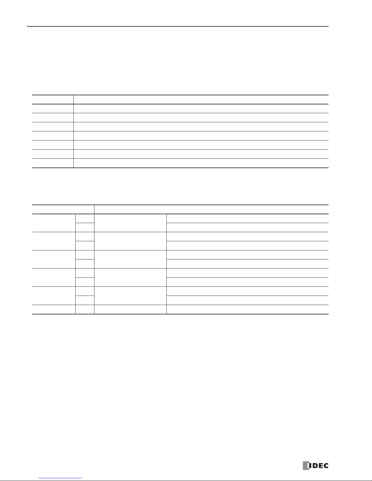
Analog Input Operating Status
The operating status of each analog input channel is stored to a data register allocated to analog input operating status.
While the analog input is operating normally, the data register stores 0. The analog input operating status data register
number is shown under Status in the Configure Parameters dialog box.
Channel
NTC Thermistor Parameters
(Values indicated on the thermistor)
Valid Range
CH0 to CH3
CH4 to CH7
R0: Thermistor resistance value at the temperature (°C) 0 to 65535
T0: Temperature (°C) –32768 to 32767
B: Thermistor B parameter (Kelvin)
0 to 65535
Analog Input Data
BT0×
BT0rR0⁄()log×+
-------------------------------------------------=
where, r = thermistor resistance (Ω)
Phone: 800.894.0412 - Web: www.clrwtr.com - Email: [email protected]
Page 36
4: ANALOG I/O CONTROL
4-14
END Refresh Type
The operating status of each analog input channel is stored to a data register, such as D761 or D767, allocated to analog
input channel 1 or 2 on analog module number 1 through 7 depending on the mounting position.
The analog input operating status data is updated whether the CPU module is running or stopped. When the CPU module
is running, the update occurs at the END processing of every scan or 10 ms, whichever is longer. When the CPU module is
stopped, the update occurs every 10 ms.
Ladder Refresh Type
The operating status of each analog input channel is stored to a data register determined by the data register number
selected in the Configure Parameters dialog box of the ANST macro.
Status Code Analog Input Operating Status (END refresh type)
0
Normal operation
1 Converting data (during the first data conversion after power-up)
2 Initializing
3 Invalid parameter or analog input channel not available on the installed analog module
4 Hardware failure (external power supply failure)
5 Incorrect wiring (input data over valid range)
6 Incorrect wiring (input data below valid range or current loop open)
Operating Status Bit Analog Input Operating Status (Ladder refresh type)
Bit 0
0
Operating status bit
Normal operation
1 Initializing, changing configuration, hardware initialization error
Bit 1
0
Parameter bit
Parameter configuration normal
1 Parameter configuration error
Bit 2
0
External power supply bit
External power supply normal
1 External power supply error
Bit 3
0
Maximum value over bit
Within the maximum value
1 Maximum value over error
Bit 4
0
Minimum value over bit
Within the minimum value
1 Minimum value under error
Bit 5 to Bit 15 0 Reserved
Normal operation
Phone: 800.894.0412 - Web: www.clrwtr.com - Email: [email protected]
Page 37
4: ANALOG I/O CONTROL
4-15
Analog Output Parameters
Analog output parameters include the analog output signal type, analog output data type, analog output minimum and
maximum values, analog output data, and analog output operating status. This section describes these parameters in detail.
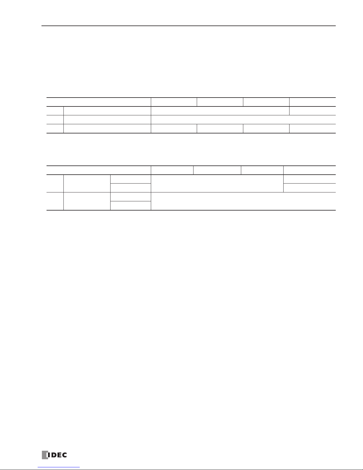
Analog Output Signal Type
A total of three analog output signal types are available, depending on the analog I/O or analog output module. Select an
analog output signal type for each analog output channel. When a channel is not used, select the default value or Not used
for the channel.
Analog Output Data Type
A total of two analog output data types are available, depending on the analog I/O or analog output module. Select an analog output data type for each analog output channel.
Analog Output Minimum/Maximum Values
For analog output values, when Optional range is selected for the Data Type, designate the analog output data minimum
and maximum values which can be –32,768 through 32,767.
Analog Output Data
The analog output data is converted into an analog output signal within the range specified by the analog output data type
and applicable parameters. The analog output data register number is shown under Data in the Configure Parameters dialog box.
END Refresh Type
The analog output data stored in a data register, such as D772, is converted into an analog output signal of voltage output
(0 to 10V DC) or current output (4 to 20 mA) as designated by the value stored in the data register allocated to analog output signal type, such as D774.
While the CPU module is running, the analog output data stored in the allocated data register is updated at the END processing of every scan or 10 ms, whichever is longer. While the CPU module is stopped, the analog output data remains at 0
or the designated analog output data minimum value, so the generated analog output signal remains at the minimum value
of 0V DC or 4 mA DC.
Ladder Refresh Type
While the CPU module is running, the analog output data stored in the allocated data register is updated when the RUNA
instruction contained in the ANST macro is executed. While the CPU module is stopped, the analog output data is not
updated. But the analog output signal can be changed by using the STPA instruction. For details, see page 4-21.
Analog Output Operating Status
The operating status of each analog output channel is stored to a data register allocated to analog output operating status.
While the analog output is operating normally, the data register stores 0. The analog output operating status data register
number is shown under Status in the Configure Parameters dialog box.
END Refresh Type
The operating status of each analog output is stored to a data register, such as D773. While the analog output is operating
normally, the data register stores 0. The analog output operating status data is updated whether the CPU module is running
or stopped. The update occurs at the END processing of every scan or 10 ms, whichever is longer.
Parameter FC4A-L03A1 FC4A-L03AP1 FC4A-K1A1 FC4A-K2C1
0 Voltage output 0 to 10V DC –10 to +10V DC
1 Current output 4 to 20 mA DC
255 Not used — — — X
Parameter FC4A-L03A1 FC4A-L03AP1 FC4A-K1A1 FC4A-K2C1
0 Binar y data
Voltage
0 to 4095
–25000 to 25000
Current 0 to 50000
1 Optional range
Voltage
Analog output data minimum value to maximum value (–32768 to 32767)
Current
Phone: 800.894.0412 - Web: www.clrwtr.com - Email: [email protected]
Page 38
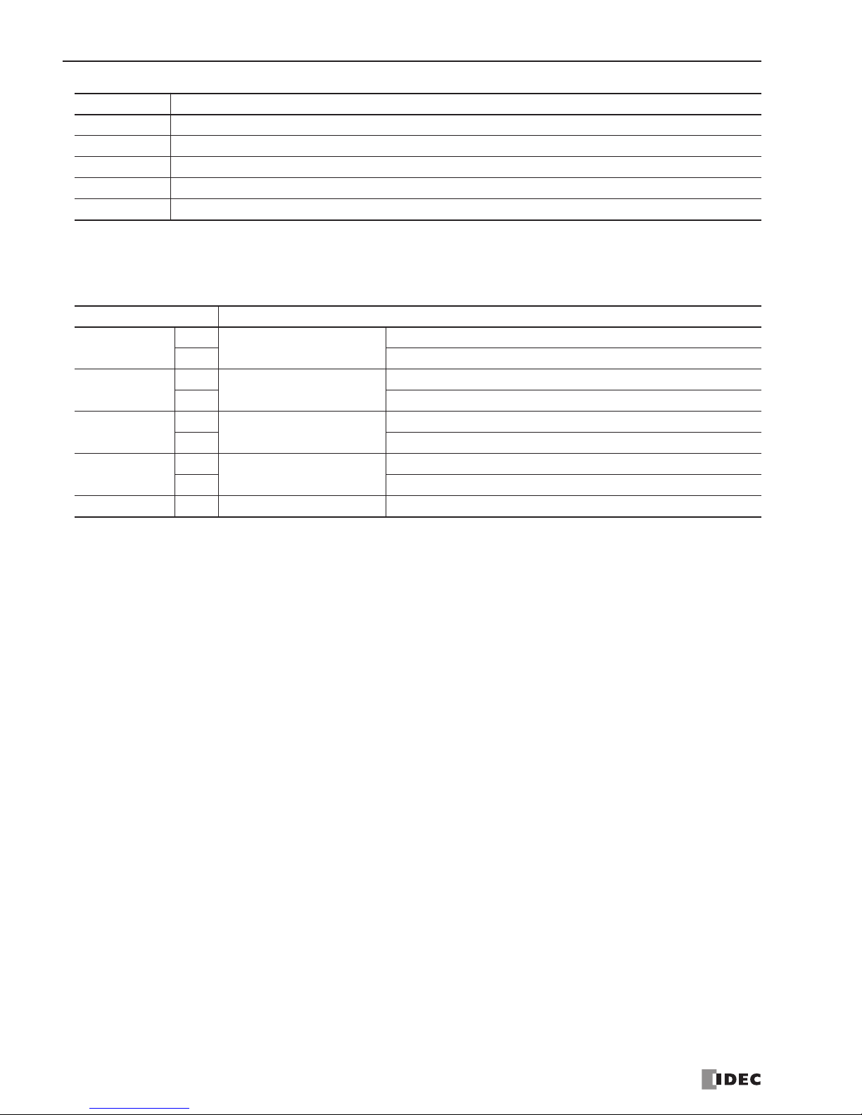
4: ANALOG I/O CONTROL
4-16
Ladder Refresh Type
The operating status of each analog output channel is stored to a data register determined by the data register number
selected in the Configure Parameters dialog box of the ANST macro.
Status Code Analog Output Operating Status (END refresh type)
0
Normal operation
1 (reserved)
2 Initializing
3 Invalid parameter or analog output channel not available on the installed analog module
4 Hardware failure (external power supply failure)
Operating Status Bit Analog Output Operating Status (Ladder refresh type)
Bit 0
0
Operating status bit
Normal operation
1 Initializing, changing configuration, hardware initialization error
Bit 1
0
Parameter bit
Parameter configuration normal
1 Parameter configuration error
Bit 2
0
External power supply bit
External power supply normal
1 External power supply error
Bit 3
0
Output data error bit
Output data normal
1 Output data range error
Bit 4 to Bit 15 0 Reserved
Normal operation
Phone: 800.894.0412 - Web: www.clrwtr.com - Email: [email protected]
Page 39
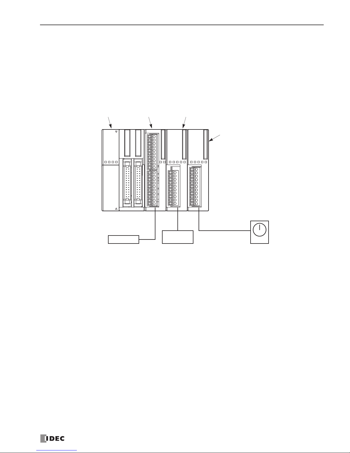
4: ANALOG I/O CONTROL
4-17
Example: Analog I/O
The following example demonstrates a program of analog I/O control using an NTC thermistor. Two analog I/O modules
are mounted in the slots shown below.
System Setup
Operation
In this example, the input value from the NTC thermistor is calibrated. When the temperature reaches the preset value, the
output is turned off. The thermistor temperature is monitored on an analog meter.
Slot No.:
1 2 3
Slim Type
CPU Module
FC4A-D40S3
Analog Input Module
(Thermistor)
FC4A-J8AT1
Output Module
(Tr. Source)
FC4A-T08S1
Thermistor
External
Device
Analog Meter
Calibrated voltage
Analog Output Module
FC4A-K1A1
Phone: 800.894.0412 - Web: www.clrwtr.com - Email: [email protected]
Page 40
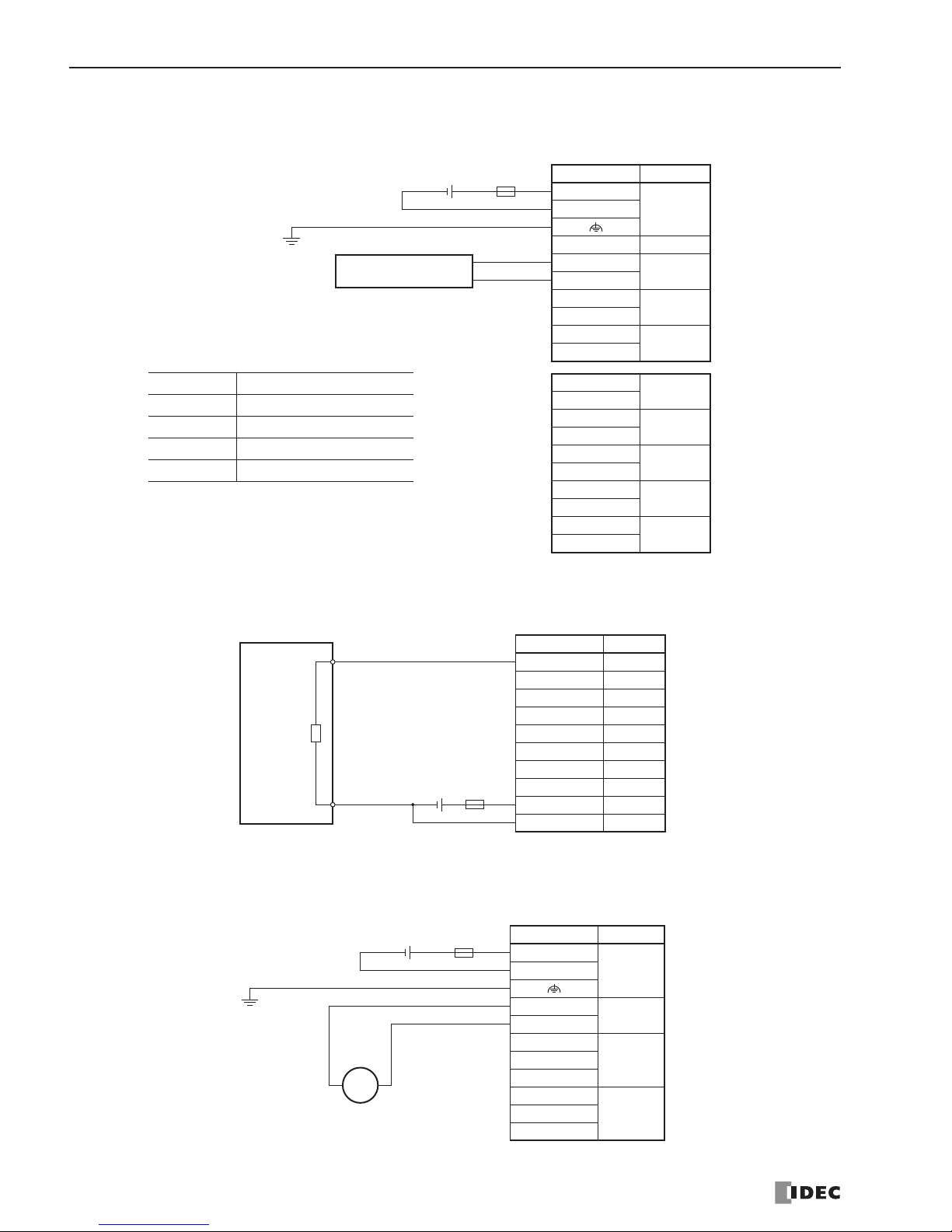
4: ANALOG I/O CONTROL
4-18
Wiring Diagram
FC4A-J8AT1 (Analog Input Module)
FC4A-T08S1 (8-point Transistor Source Output Module)
FC4A-K1A1 (Analog Output Module)
Terminal No. Channel
24V
24V DC0V
NC —
A
IN0
B
A
IN1
B
A
IN2
B
A
IN3
B
A
IN4
B
A
IN5
B
A
IN6
B
A
IN7
B
Fuse
+–
24V DC
NTC Thermistor
B
A
• Thermistor Specifications
Type No. NT731ATTD103K38J (KOA)
Type NTC
RO 10,000Ω
T0 298K (25°C)
B Parameter 3,800K
T
erminal No. Output
0 Q0
1 Q1
2 Q2
3 Q3
4 Q4
5 Q5
6 Q6
7 Q7
COM(+) COM(+)
–V –V
Fuse
+–
External
Device
+IN
–IN
Terminal No. Channel
+
24V DC–
+
OUT
–
NC
—NC
NC
NC
—NC
NC
Fuse
+–
24V DC
+ –
Analog Meter
V
Phone: 800.894.0412 - Web: www.clrwtr.com - Email: [email protected]
Page 41
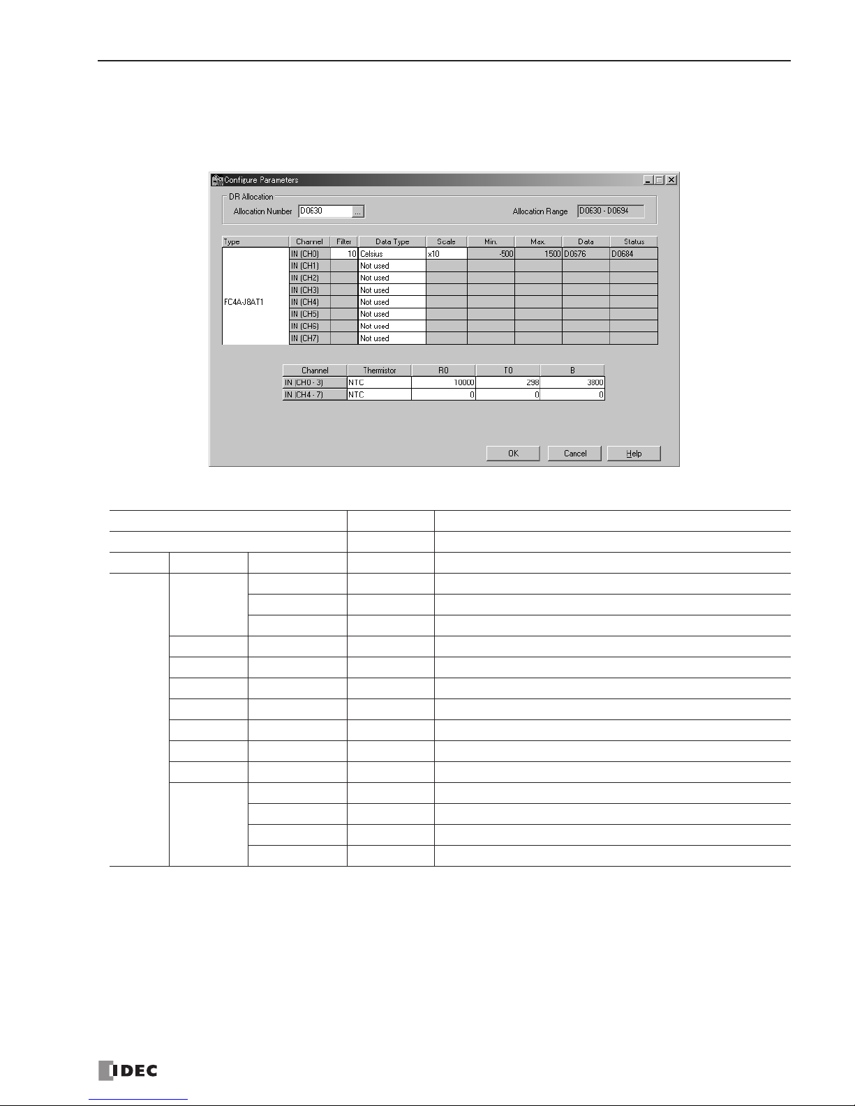
4: ANALOG I/O CONTROL
4-19
WindLDR Programming
Analog I/O modules are programmed using the ANST macro in WindLDR. Program the ANST macro as shown below.
• Analog Input Module FC4A-J8AT1 on Slot 1
Note: When CH4 through CH7 are not used, thermistor settings are not required.
DR Allocation Range Designation Description
D630 - D694 D630 Optional range allocation, 65 words
I/O Channel Item Designation Description
IN
CH0
Filter 10 Averages input values
Data Type Celsius Analog input range –50 to 150°C
Scale
×10 Analog input data –500 to 1500
CH1 Data Type Not used Unused channel
CH2 Data Type Not used Unused channel
CH3 Data Type Not used Unused channel
CH4 Data Type Not used Unused channel
CH5 Data Type Not used Unused channel
CH6 Data Type Not used Unused channel
CH7 Data Type Not used Unused channel
CH0 - CH3
Thermistor Type NTC NTC thermistor
R0 10,000 Resistance value at the absolute temperature = 10 k
Ω
T0 298 Absolute temperature = 298K (25°C)
B 3,800
B parameter = 3,800K
Phone: 800.894.0412 - Web: www.clrwtr.com - Email: [email protected]
Page 42
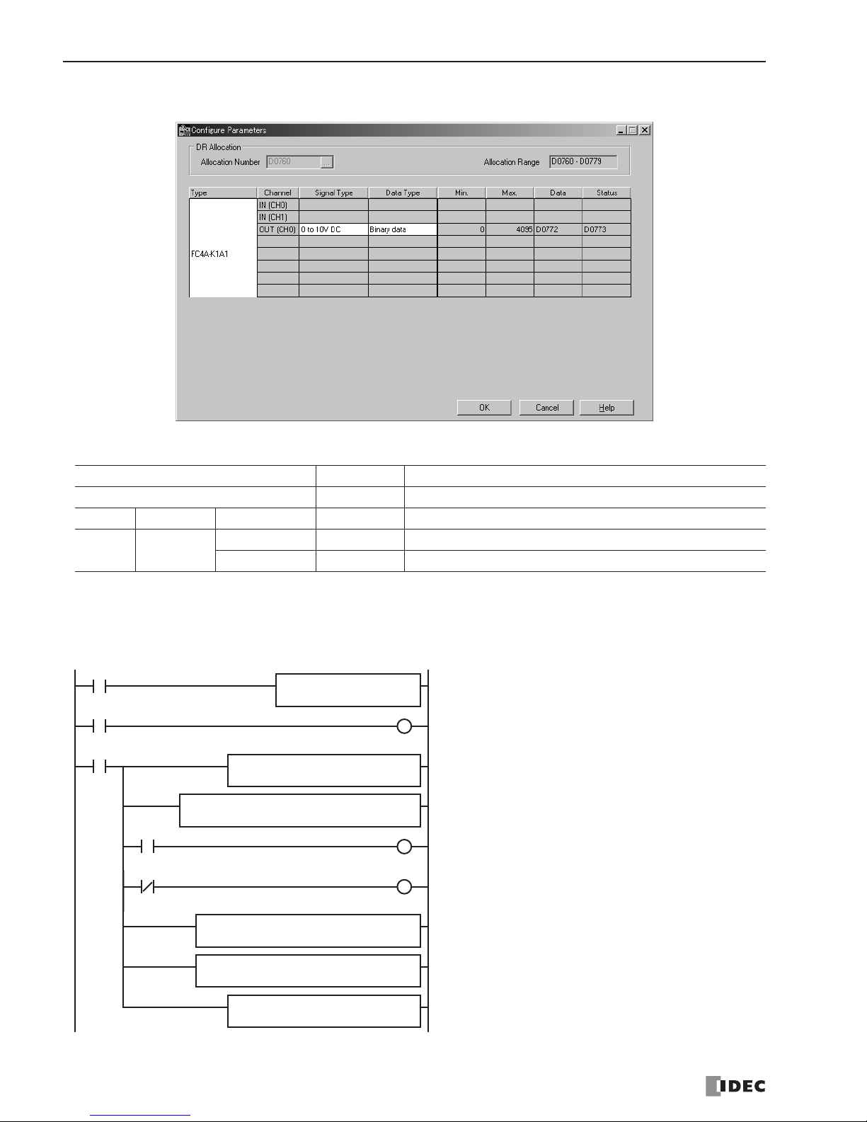
4: ANALOG I/O CONTROL
Note: The above ladder diagram is only an example and should be modified as required.
4-20
• Analog Output Module FC4A-K1A1 on Slot 3
Ladder Diagram
As shown in the ladder diagram below, when initialize pulse special internal relay M8120 is used for the ANST macro in
parallel with another instruction, load M8120 again for the other instruction.
DR Allocation Range Designation Description
D760 - D779 — Automatic range allocation, 20 words
I/O Channel Item Designation Description
OUT CH0
Signal Type 0 to 10V DC Voltage output
Data Type Binary data
0 to 4095
M8120 is the initialize pulse special internal relay.
When the CPU starts to run, ANST stores parameters to
data registers to configure analog I/O modules and Q30
is turned on.
When I0 is turned on, analog input data is moved from
D676 to D1000.
The temperature is compared with the alarm temperature of 100°C.
When the temperature is higher than 100°C, Q30 is
turned off.
When the temperature is not higher than 100°C, Q30 is
turned on.
Analog input data of –500 to +1500 is converted to 0 to
2000.
Analog input data of 0 to 2000 is converted to 0 to
4000.
Analog input data of 0 to 4000 is moved to D772 (analog output data) of the analog output module.
M8120
REPS1 –
D676
D1 –
D1000
MOV(I)
REPS1 –
D1000
D1 –
D772
MOV(W)
REPS1 –
D676
D1 –
M30
CMP>(I)
S2 –
1000
NO.1
J8AT1
NO.3
K1A1
ANST
Q30
S
Q30
R
Q30
S
M30
M30
I0
REPS2 –
500
D1 –
D1000
S1 –
D1000
ADD(I)
REPS2 –2D1 –
D1000
S1 –
D1000
MUL(W)
M8120
Phone: 800.894.0412 - Web: www.clrwtr.com - Email: [email protected]
Page 43
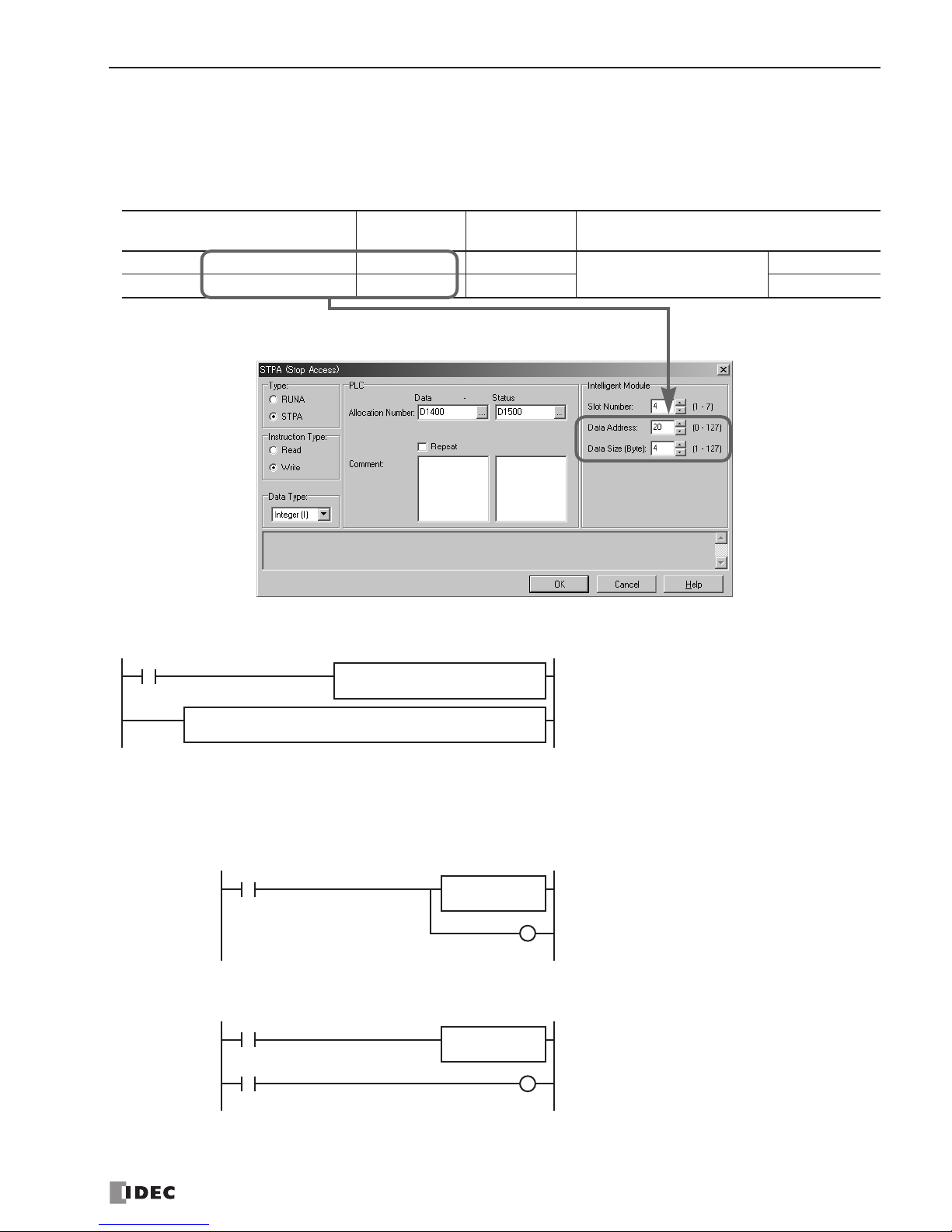
4: ANALOG I/O CONTROL
4-21
Changing Analog Output While CPU is Stopped
When using the FC4A-K2C1 analog output module, the analog output value can be changed while the CPU module is
stopped. To change the analog output value, store a required output value to the memory addresses allocated to the analog
output data.
Example: Memory Allocation of Ladder Refresh Type Analog Output Module FC4A-K2C1
STPA instruction when FC4A-K2C1 is mounted on slot 4
Ladder Diagram
Note: The above ladder diagram is only an example and should be modified as required.
Precautions for Programming ANST Macro
When using the ANST macro, do not make a branch from the ladder line of the ANST macro.
Delete the branch from the ANST macro, and start another line by inserting a LOD instruction.
Memory Address
(data address used for STPA)
Data Size
(bytes)
R/W Parameter
+20 2 R/W
Analog Output Data
CH0
+22 2 R/W CH1
M8120 is the initialize pulse special internal
relay.
MOV stores output values at the OFF state.
When the CPU stops, STPA updates the analog
output value of the analog output module.
M8120
REP
2
S1 –0D1 R
D1400
MOV(I)
DATA
D1400
SLOT
4
STATUS
D1500
BYTE
4
ADDRESS
20WRITE
STPA(I)
M8120
NO.1
J8AT1
ANST
Q1
Incorrect
M8120
NO.1
J8AT1
ANST
Q1M8120
Correct
Phone: 800.894.0412 - Web: www.clrwtr.com - Email: [email protected]
Page 44
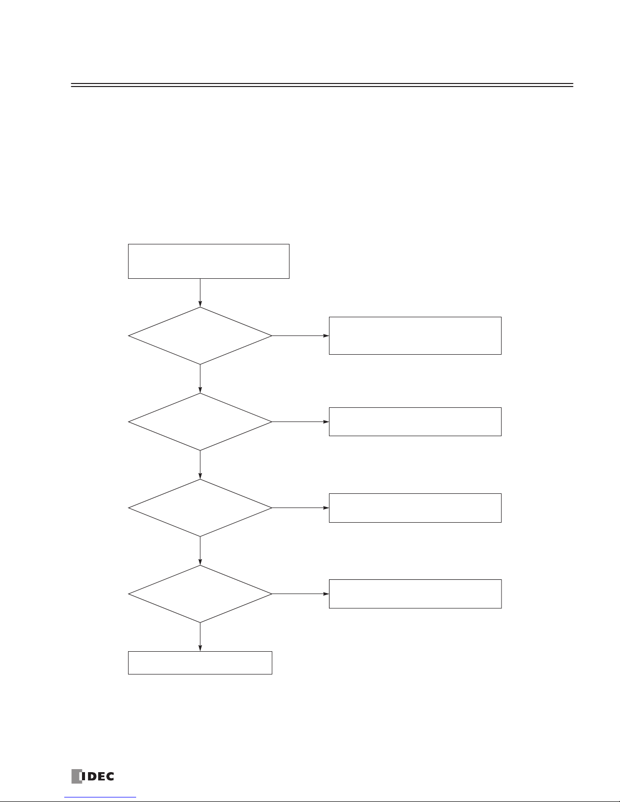
5-1
5: TROUBLESHOOTING
Introduction
This chapter describes the procedures to determine the cause of trouble and actions to be taken when any trouble occurs
while operating the analog I/O modules. When a trouble occurred, check the points and take the actions described below.
If the trouble cannot be solved, call IDEC for assistance.
Troubleshooting Diagrams
Analog I/O module does not work correctly (END Refresh Type)
YES
NO
NO
YES
Does the Status
DR store status code 4
(hardware failure)?
Call IDEC for assistance.
Analog I/O module does not work
correctly (END Refresh Type).
Make sure of correct parameters.
YES
NO
After changing settings,
was the CPU stopped and
restarted?
Stop and restar t the CPU to configure the
analog I/O settings.
Supply the rated power voltage to the
analog I/O module.
See pages 4-14 and 4-16.
Does the Status
DR store status code 3
(invalid parameter)?
YES
NO
Are data registers
duplicated?
Change data register numbers to
eliminate duplicated data registers.
Phone: 800.894.0412 - Web: www.clrwtr.com - Email: [email protected]
Page 45
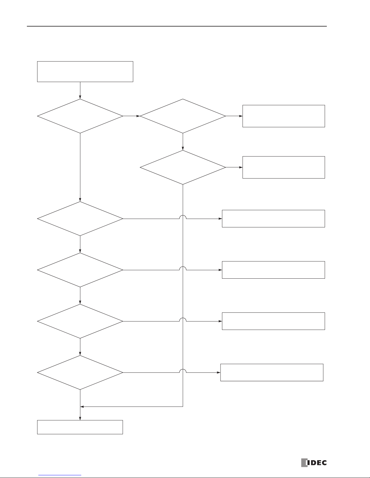
5: TROUBLESHOOTING
5-2
Analog I/O module does not work correctly (Ladder Refresh Type)
NO
YES
NO
YES
Is the status LED turned on?
Call IDEC for assistance.
Analog I/O module does not work
correctly (Ladder Refresh Type).
Make sure of correct parameters.
YES
After changing settings,
was the CPU stopped and
restarted?
Stop and restar t the CPU to configure the
analog I/O settings.
Supply the rated power voltage
to the analog I/O module.
See pages 4-14 and 4-16.
Does the Status
DR store status code 2
(parameter configuration
error)?
NO
Are data registers
duplicated?
Change data register numbers to
eliminate duplicated data registers.
Does the Status
DR store status code 4
(external power supply
error)?
NO
Program M8120 (initialize pulse)
as an input for the ANST macro,
and stop and restar t the CPU.
Does the Status
DR store status code 1
(initializing)?
NO
YES
YES
NO
Is “Not used” selected
for the Signal Type?
Select a required Signal Type for the
channel to be used.
YES
NO
YES
Phone: 800.894.0412 - Web: www.clrwtr.com - Email: [email protected]
Page 46

i
A analog
I/O
control 4-1
data 4-3, 4-6
module specifications 2-2
module type numbers 1-1
modules 1-1
operating status 4-3, 4-6
input
data 4-13
data type 4-11
minimum/maximum values 4-13
operating status 4-13
parameters 4-11
signal type 4-11
output
changing 4-21
data 4-15
data type 4-15
minimum/maximum values 4-15
operating status 4-15
parameters 4-15
signal type 4-15
ANST 4-2
applicable
CPU modules 1-2
WindLDR version 1-2
C Celsius 4-12
changing analog output 4-21
confirming system program version 1-2
crimping tool 3-2
D data register for analog I/O modules 4-8
dimensions 2-14
direct mounting strip 3-1
E END refresh type 1-1
example 4-17
F Fahrenheit 4-12
ferrule 3-2
filter value 4-13
G general
information 1-1
specifications 2-2
I installation and wiring 3-1
L ladder refresh type 1-1
M module specifications 2-1
mounting hole layout for direct mounting 3-1
O operating status 4-3
P parts description 2-1
Phoenix 3-2
PID instruction source operand S4 4-3
PLC status 1-2
power supply 2-13
precautions for programming ANST macro 4-21
programming WindLDR 4-2
protection type 2-12
R resistance 4-12
S screwdriver 3-2
specifications
analog
I/O module 2-2
input 2-3, 2-4, 2-6
output 2-7
general 2-2
system program version D8029 1-2
T terminal
arrangement 2-8
connection 3-2
thermistor parameter 4-13
tightening torque 3-2
troubleshooting 5-1
diagrams 5-1
type
numbers analog I/O module 1-1
of protection 2-12
W WindLDR
programming 4-2
version 1-2
wiring 3-1
diagrams 2-8
INDEX
Phone: 800.894.0412 - Web: www.clrwtr.com - Email: [email protected]
 Loading...