

Datasheet PA7024JN-25, PA7024JN-20, PA7024JN-15, PA7024JI-20, PA7024JI-15 Datasheet (ICT)
...
1 of 6
PA7024
PA7024 PEEL
TM
Array
Programmable Electrically Erasable Logic A rray
■
CMOS Electrically Erasable Technology
- Reprogrammable in 24-pin DIP, SOIC and
28-pin PLCC packages
-Optional JN package for 22V10 power/ground
compatibility
■
Most Powerful 24-pin PLD Available
- 20 I/Os, 2 inputs/clocks, 40 registers/latches
- 40 logic cell output functions
- PLA structure with true product-term sharing
- Logic functions and registers can be I/O-buried
■
Flexible Logic Cell
- Multiple output functions per cell
- D,T and JK registers with special features
- Independent or global clocks, resets, presets,
clock polarity and output enables
-Sum of products logic for output enable
■
High-Speed Commercial and Industrial Versions
- As fast as 10ns/15ns (tpdi/tpdx), 71.4MHz (fMAX)
- Industrial grade available for 4.5 to 5.5V Vcc
and -40 to +85°C temperatures
■
Ideal for Comb in at orial, Synchronous and
Asynchrono us Lo gi c Applications
- Integration of multiple PLDs and random logic
- Buried counters, complex state-machines
- Comparators, decoders, multiplexers and
other wide-gate functions
■
Development and Programmer Support
- ICT PLACE Development Software
- Fitters for ABEL, CUPL and other software
-Programming support by ICT PDS-3 and popular thirdparty programmer s
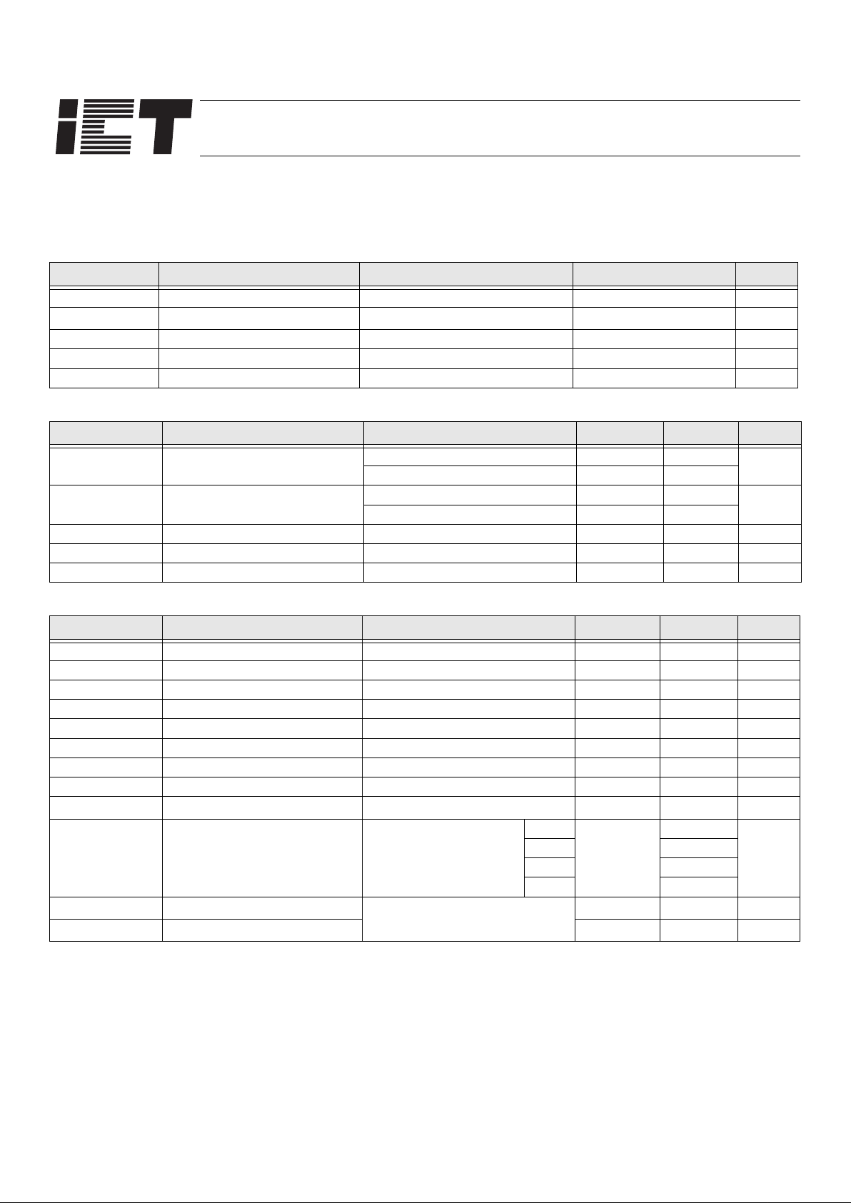
The PA70 24 is a member of the Programmable Electrical ly
Erasable Logic (PEEL™) Array family based on ICT’s
CMOS EEPROM technology. PEEL™ Arrays free designers from the limitations of ordina ry PLDs by providing the
architectural flexibility and speed needed for today’s programmable logic designs. The PA7024 is by far the most
powerful 24-pin PLD available today with 20 I/O pins, 2
input/global-clocks and 40 registers/latches (20 buried logic
cells and 20 I/O registers/latches). Its logic array implements 84 sum-of-product logic functions that share 80
product terms. The PA7024’s logic and I/O cells (LCCs,
IOCs) are extremely flexible, offering two output functions
per logic cell (a total of 40 for all 20 logic cells). Logic cells
are configurable as D, T, and JK registers w ith indepe ndent
or global clocks, resets, presets, clock polarity, and other
special features. This makes them suitable for a wide variety of combinator ial, synchronous an d asynchrono us logic
applications. With pin compatib ility and super-set functionality to most 24-pin PLDs, (22V10, EP610/630, GAL6002),
the PA7024 c an implement designs that exceed the architectures of such devices. The PA7024 suppor ts speeds as
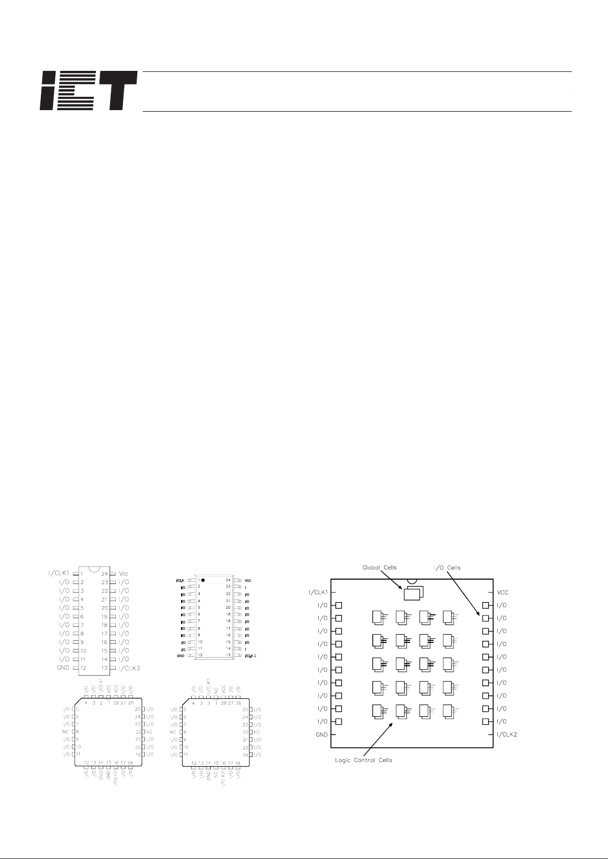
fast as 10ns/15ns (tpdi/tpdx) and 71.4MH z (fMAX) at moderate power consumption 120mA (85mA typical). Packaging includes 24-pin DIP, SOIC and 28-pin PLCC (see Figure
1). Development and programming suppor t for the PA7024
is provided by ICT and popular third-party development tool
manufacturers.
General Description
Features
DIP
PLCC-J
PLCC-JN
SOIC
Figur e 1: Pin Configuration Figur e 2. Block Diagram
Commercial/
Industrial
2 of 6
PA7024
Table 1. Absolute Maximum Ratings
Symbol Parameter Conditions Ratings Unit
V
CC
Supply Voltage Relative to Ground -0.5 to + 7.0 V
V
I
, V
O
Voltage Applied to Any Pin
2
Relative to Ground
1
-0.5 to VCC + 0.6 V
I
O
Output Current Per pin (IOL, IOH)±25mA
T
ST
Storage Temperature -65 to + 150 °C
T
LT
Lead Temperature Soldering 10 seconds +300 °C
Table 2. Operating Ranges
Symbol Parameter Conditions Min Max Unit
V
CC
Supply Voltage
Commercial 4.75 5.25
V
Industrial 4.5 5.5
T
A
Ambient Temperature
Commercial 0 +70
°C
Industrial -40 +85
T
R
Clock Rise Time See Note 2 20 ns
T
F
Clock Fall Time See Note 2 20 ns
T
RVCC
V
CC
Rise Time See Note 2 250 ms
Table 3. D.C. Electrical Characteristics over the recommended operating conditions
Symbol Parameter Conditions Min Max Unit
V
OH
Output HIGH Voltage - TTL VCC = Min, IOH = -4.0mA 2.4 V
V
OHC
Output HIGH Voltage - CMOS VCC = Min, IOH = -10µA VCC - 0.3 V
V
OL
Output LOW Voltage - TTL V
CC
= Min, I
OL
= 16mA 0.5 V
V
OLC
Output LOW Voltage - CMOS VCC = Min, IOL = 10µA 0.15 V
V
IH
Input HIGH Leve l 2.0 VCC + 0.3 V
V
IL
Input LOW Level -0.3 0.8 V
I
IL
Input Le ak ag e C ur re n t V
CC
= Max, GND ≤ V
IN
≤
V
CC
±10 µA
I
OZ
Outp ut Le ak ag e C urr e nt I/O = High- Z , GN D ≤ V
O
≤
V
CC
±10 µA
I
SC
Output Short Circuit Current
4
VCC = 5V, VO = 0.5V, TA= 25°C -30 -120 mA
I
CC
11
VCC Current
V
IN
= 0V or V
CC
3,11
f = 25MHz
All outputs disabled
4
-15
85 (typ.)
17
120
mA
-20 120
-25 120
I-25 130
C
IN
7
Input Capacitance
5
TA = 25°C, VCC = 5.0V
@ f = 1 MHz
6pF
C
OUT
7
Output Capacitance
5
12 pF
This device has been designed and tested for the recommended
operating conditions. Proper operation outside these levels is not
guaranteed. Exposure to absolute maximum ratings may cause permanent damage.

3 of 6
PA7024
Table 1. A.C Electrical Characteristics Combinatorial
Symbol Parameter
6,12
-15 -20 I -25
UnitMin Max Min Max Min Max
t
PDI
Propagation de lay Internal (t
AL + tLC)
10 13 17 ns
t
PDX
Propagation de lay External (tIA + tAL +tLC + tLO)15 20 25ns
t
IA
Input or I/O pin to array input 2 2 2 ns
t
AL
Arra y input to LCC 9 12 16 ns
t
LC
LCC input to LCC output
10
11 1ns
t
LO
LCC output to output pin 3 5 6 ns
t
OD
, t
OE
Output Disable, Enable from LCC output
7
35 6ns
t
OX
Output Disable, Enable from input pin
7
15 20 25 ns
Combinatorial Timing - Waveforms and Block Diagram
Over the operating range

4 of 6
PA7024
Table 1. A.C. Electrical Characteristics Sequential over the operating range
Symbol
Parameter
6,12
-15 -20 I-25
Unit
Min Max Min Max Min Max
t
SCI
Internal set-up to system clock8 - LCC14
(t
AL
+ tSK + tLC - tCK)
6 9 15 ns
t
SCX
Input
16
(EXT.) set-up to system clock, - LCC (t
IA + tSCI)
81117ns
t
COI
System-clock to Array Int. - LCC/IOC/INC
14
(t
CK +tLC
)
888ns
t
COX
System-clock to Output Ext. - LCC (t
COI
+ tLO) 121313ns
t
HX
Input hold time from system clock - LCC 0 0 0 ns
t
SK
LCC Input set-up to async. clock
13
- LCC
334ns
t
AK
Clock at LCC or IOC - LCC output 1 1 1 ns
t
HK
LCC input hold time from sys tem clock - LCC 4 4 4 ns
t
SI
Input set-up to system clock - IOC/INC14 (tSK - tCK)
000ns
t
HI
Input hold time from system clock - IOC/INC14 (tSK - tCK)
444/3ns
t
PK
Array input to IOC PCLK clock 6 7 9 ns
t
SPI
Input set-up to PCLK clock18 - IOC/INC (tSK-tPK-tIA)
16
000ns
t
HPI
Inpu t hold from PCLK clock18 - IOC/INC (tPK+tIA-tSK)
16
567ns
t
CK
System-clock delay to LCC/IOCINC 7 7 7 ns
t
CW
System-clock low or high pulse width 7 7 8 ns
f
MAX
1 Max. system-clock frequency Int/I nt 1/(t
SCI
+ t
COI
) 71.4 58.8 43.5 MHz
f
MAX
2 Max. system-clock frequency Ext/I nt 1/(t
SCX
+ t
COI
) 62. 5 52.6 40.0 MHz
f
MAX
3 Max. system-clock frequency Int/Ex t 1/(t
SCI
+ t
COX
) 55.5 45.5 35.7 MHz
f
MAX
4 Max. system-clock frequency Ext/Ex t 1/(t
SCX
+ t
COX
) 50.0 4 1.6 33.3 MHz
f
TGL
Max. sy stem-clock toggle frequency 1/(tCW + tCW)
9
71.4 71.4 62.5 MHz
t
PR
LCC presents/reset to LCC output 1 1 2 ns
t
ST
Input to Global Cell present/reset (
tIA
+ tAL + tPR) 121520ns
t
AW
Async h. preset/reset pulse w idth 8 8 8 ns
t
RT
Inpu t to LCC Reg-Type (RT ) 6 8 10 ns
t
RTV
LCC Reg-Type to LCC output r e giste r change 1 1 2 ns
t
RTC
Input to Global Cell register-type change (tRT + t
RTV
)7912ns
t
RW
Async h. Reg-Type pulse width 10 10 10 ns
t
RESET
Power- on reset time for registers in clea r state
2
555µs

5 of 6
PA7024
Sequential Timing - Waveforms and Block Diagram
Notes
1. Minim u m D C in pu t is - 0.5V, howev e r in pu t s ma y u nd er sh oot to -2. 0 V f o r
periods less than 2 0ns.
2. Test points for Clock and V
CC
in tR,tF,tCL,tCH, and t
RESET
are referenced
at 10% an d 90% levels.
3. I/O p ins are 0V or V
CC
.
4. Test one output at a time for a duration of less than 1 sec.
5. Capacitances are te sted on a sample basis.
6. Test conditions assume: signal transition times of 5ns or less from the
10% and 90% point s, timing reference levels of 1.5V (unless otherwise
specified).
7. t
OE
is measured from input transition to V
REF
±0.1V (See test loads for
V
REF
value). t
OD
is measured from input tran sition to V
OH
-0.1Vor V
OL
+0.1V.
8. “System-clock” refers to pin 1 or 13 (2 or 16 PLCC) high speed clocks.
9. For T or JK registers in toggle (divide by 2) operation only.
10. For combinatorial and async-clock to LC C output delay.
11. I
CC
for a typical application: This parameter is tested with the device
programmed as a 10-bi t D-type counter.
12. Test loads are specified in Sectio n 5 of this Data Book.
13. “Async. clock” refers to the clock from the Sum term (OR gate).
14. The “LCC” term indicates that the timing parameter is app lied to the
LCC register. The “IOC” term indicates that the timing parameter is
applied to the IOC register. The “LCC/IOC/INC” term indicates that the
timing parameter is applied to both the LCC, IOC an d INC registers .
15. The term “Inp ut” without any reference to another term refers to an
(external) input pi n.
16. Th e p ar am e ter t
SPI
indicates that the PCLK signal to the IOC register is
alwa ys sl o wer th an th e d at a fr o m the pi n o r inpu t by the absolute v a lu e
of (t
SK -tPK -tIA
). This means that no set-up time for the data from the
pin or input is required, i.e . the external data and clock can be sent to
the device simultaneou s ly. Additionally, the data fr om the pin must
remain stable for t
HPI
time, i.e. to wait for the PCLK signal to arrive at
the IOC register.
17. Typical (typ) I
CC
is measured at TA =25°C, Freq = 25MHz, V
CC
=5V.

6 of 6
PA7024
Ordering Information
Part Number Speed Temperature Package
PA7024P-15
10/15ns C
P24
PA7024J-15 J28
PA7024JN-15 JN28
PA7024S-15 S24
PA7024P-20
13/20ns C
P24
PA7024J-20 J28
PA7024JN-20 JN28
PA7024S-20 S24
PA7024PI-25 17/25ns I P24
PA7024JI-25 17/25ns I J28
PA7024JNI-25 17/25ns I JN28
PA7024SI-25 17/25ns I S24
Part Number
Device
PA702 4J-20
Package
P = Plastic 300mil DIP
J = Plastic (J) Leaded Chip Carrier
JN = PLCC Alternate Pin Out
S = SOIC 300mil Gullwing
Temperature Range
(Blank) = Comme rcial 0 to 70°C
I = Indu stria l - 4 0 to + 8 5°C
Speed
-15 = 10ns/15ns tpdi/tpdx
-20 = 13ns/20ns tpdi/tpdx
-25 = 17ns/25ns tpdi/tpdx
Suffix
 Loading...