PRELIMINARY INFORMATION
Quad 1 to 4 Buffalo™ Clock Driver
MK74CB44
Description
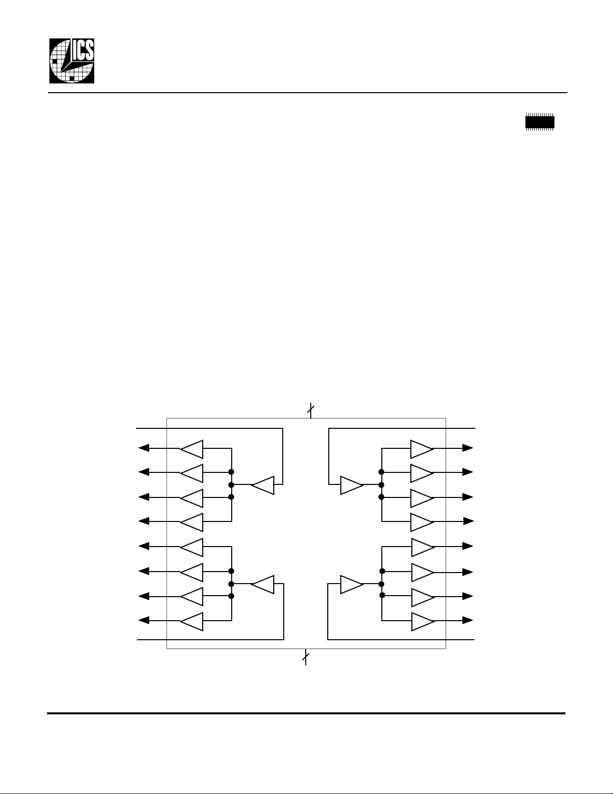
The MK74CB44 Buffalo™ is a monolithic
CMOS high speed clock driver. It consists of
four identical single input to four low-skew
output, non-inverting clock drivers. When
combined with ICS’s MK series of low jitter
clock synthesizers, the chips form an unequaled
high performance clocking scheme. This
monolithic solution can eliminate concern for
part-to-part skew matching. The MK74CB44 is
packaged in the tiny 28 pin SSOP, which uses the
same board space as the narrow 16 pin SOIC.
Block Diagram
INA
Features
• Tiny 28 pin SSOP (150 mil) package
• Quad one input to four output clock drivers
• Outputs are skew matched to within 250ps
• A, B, C and D banks matched to 250ps
• 3.3V±10% and/or 5V±10% supply voltage
• Clock speeds up to 200 MHz
• For tighter skew matching, more outputs, or
other speeds, consult ICS for other solutions
Family of ICS Parts
The MK74CB44 Buffalo™ is designed to be used
with ICS’s clock synthesizer devices. The inputs
of the Buffalo are matched to the outputs of ICS
clock synthesizers. Consult ICS for applications
support.
VDD
4
IND
QA0
QA1
QA2
QA3
QB0
QB1
QB2
QB3
INB INC
4
GND
MDS 74CB44 B 1 Revision 022000 Printed 11/17/00
Integrated Circuit Systems, Inc. • 525 Race St. • San Jose • CA • 95126 • (408)295-9800tel • www.icst.com
QD0
QD1
QD2
QD3
QC0
QC1
QC2
QC3

PRELIMINARY INFORMATION
Quad 1 to 4 Buffalo™ Clock Driver
MK74CB44
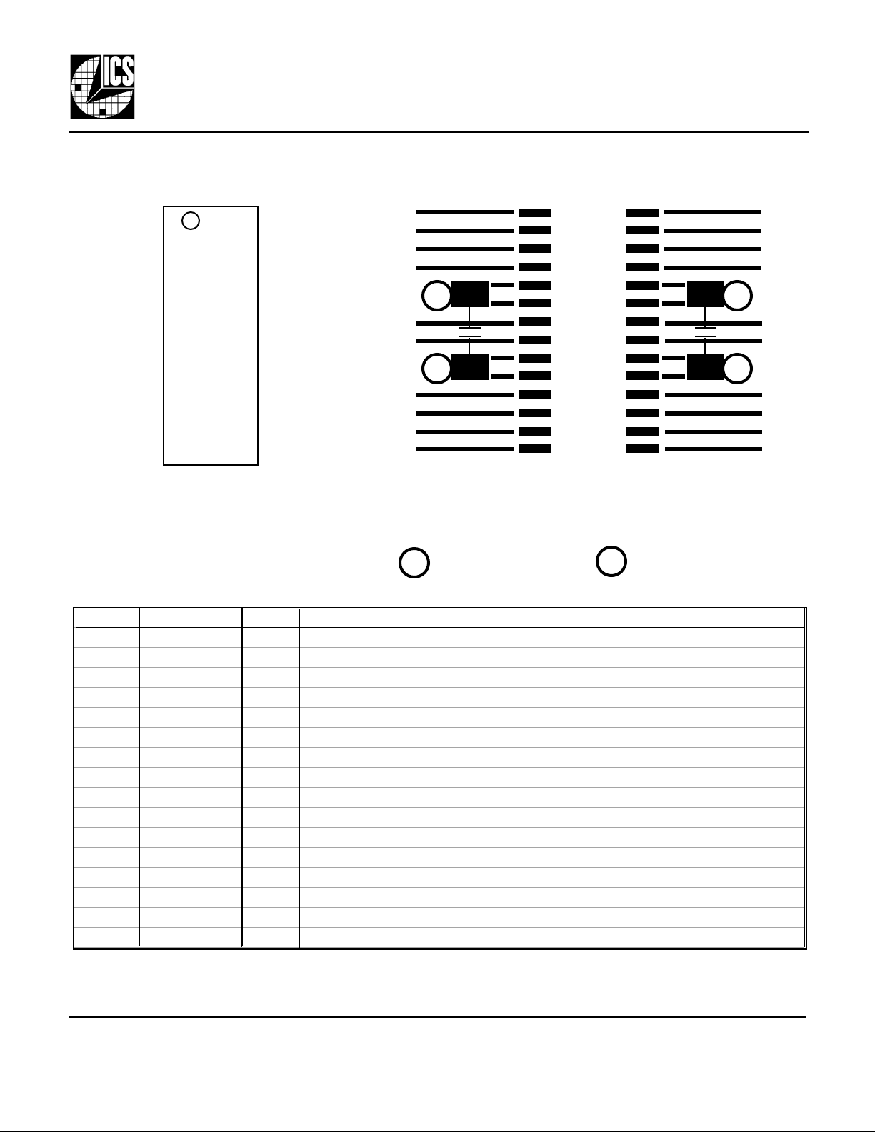
Pin Assignment
1
INA
2
QA0
QA1
3
QA2
4
QA3
QB0
QB1
QB2
QB3
INB
5
6
7
8
9
10
11
12
13
14
VDD
VDD
GND
GND
28
27
26
25
24
23
22
21
20
19
18
17
16
15
IND
QD0
QD1
QD2
VDD
VDD
QD3
QC0
GND
GND
QC1
QC2
QC3
INC
0.01µF
Suggested Layout
V
G
For simplicity,series terminating resistors (required) are not
shown for the outputs, but should be placed as close to the
device as possible. It is most critical to have the 0.01µF
decoupling capacitors closest.
= connect to VDD
V
= connect to GNDG
V
0.01µF
G
Pin Descriptions
Number Name Type Description
1 INA I Clock input for four A outputs.
2, 3, 4 QA0, QA1, QA2 O Clock A outputs.
5, 6 VDD P Power supply. Connect to +3.3 V or +5 V. Must be the same as pins 23, 24.
7 QA3 O Clock A output.
8 QB0 o Clock B output.
9, 10 GND P Connect to ground.
11, 12, 13 QB1, QB2, QB3 O Clock B outputs.
14 INB I Clock input for four B outputs.
15 INC I Clock input for four C outputs.
16, 17, 18 QC3, QC2, QC1 O Clock C outputs.
19, 20 GND P Connect to ground.
21 QC0 O Clock C output.
22 QD3 O Clock D output.
23, 24 VDD P Power supply. Connect to +3.3 V or +5 V. Must be the same as pins 5, 6.
25, 26, 27 QD2, QD1, QD0 O Clock D outputs.
28 IND I Clock input for four D outputs.
Type: I = Input, O = output, P = power supply connection
MDS 74CB44 B 2 Revision 022000 Printed 11/17/00
Integrated Circuit Systems, Inc. • 525 Race St. • San Jose • CA • 95126 • (408)295-9800tel • www.icst.com
 Loading...