ICST MK74CB217RTR, MK74CB217R Datasheet

PRELIMINARY INFORMATION
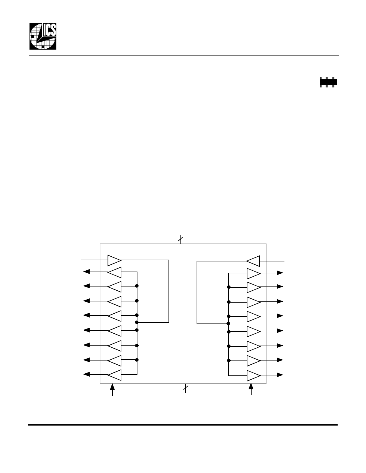
Dual 1 to 8 Buffalo™ Clock Driver
MK74CB217
Description
The MK74CB217 Buffalo™ is a monolithic
CMOS high speed clock driver. It consists of two
identical single input to eight low-skew output,
non-inverting clock drivers. This eliminates
concerns of part to part matching in many
systems. The MK74CB217 is packaged in the
tiny 28 pin SSOP, which uses the same board
space as the narrow 16 pin SOIC. The inputs can
be connected together for a 1 to 16 fanout buffer.
A quad 1 to 4, and PECL versions, are also
available. Consult us for more details.
Block Diagram
Features
• Tiny 28 pin SSOP (150 mil) package
• Dual one input to eight output clock drivers
• Outputs are skew matched to within 250 ps
• A outputs and B outputs matched to 250 ps
• 3.3 V or 5 V supply voltage
• Output Enable tri-states each bank of eight
• Clock speeds up to 200 MHz
Family of ICS Parts
The MK74CB217 Buffalo™ is designed to be used
with ICS’s clock synthesizer devices. The inputs of the
Buffalo are matched to the outputs of ICS clock
synthesizers. Consult ICS for applications support.
VDD
4
INA
QA0
QA1
QA2
QA3
QA4
QA5
QA6
QA7
4
OEA (all A outputs)
GND
MDS74CB217A 1 Revision 12299 Printed 2/22/00
IntegratedCircuit Systems, Inc. • 525 Race Street • San Jose •CA •95126•(408) 295-9800tel • www.icst.com
OEB (all B outputs)
INB
QB0
QB1
QB2
QB3
QB4
QB5
QB6
QB7

PRELIMINARY INFORMATION
Dual 1 to 8 Buffalo™ Clock Driver
MK74CB217
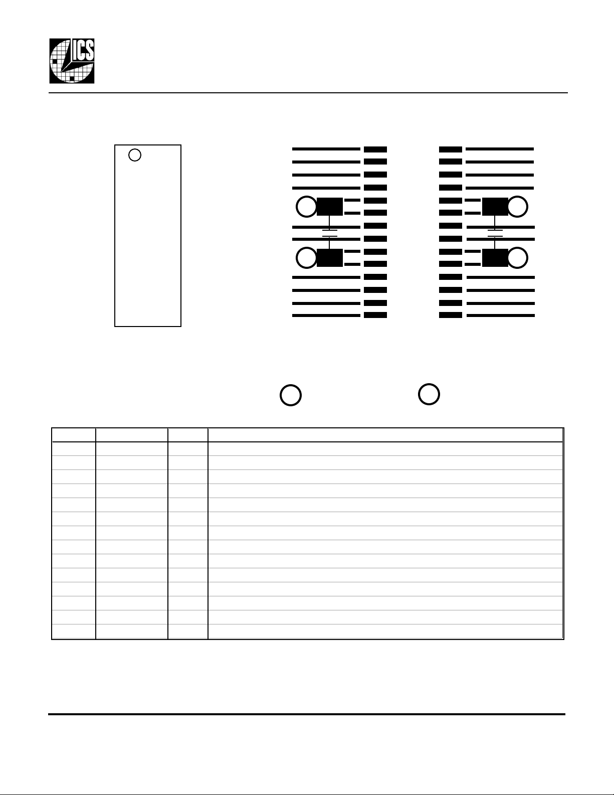
Pin Assignment
INA
1
QA0
2
QA1
3
QA2
4
QA3
QA4
QA5
QA6
QA7
OEA
5
6
7
8
9
10
11
12
13
14
VDD
VDD
GND
GND
28
27
26
25
24
23
22
21
20
19
18
17
16
15
INB
QB0
QB1
QB2
VDD
VDD
QB3
QB4
GND
GND
QB5
QB6
QB7
OEB
Suggested Layout
V
0.1µF
G
For simplicity, terminating resistors are not shown for the
outputs, but should be placed as close to the device as
possible. It is most critical to have the 0.1µF decoupling
capacitors closest.
= connect to VDD
V
= connect to GND
G
V
0.1µF
G
Pin Descriptions
Number Name Type Description
1 INA I Clock input for eight A outputs.
2, 3, 4 QA0, QA1, QA2 O Clock A outputs.
5, 6 VDD P Power supply. Connect to 3.3 V or +5 V. Must be same as pins 23, 24.
7, 8 QA3, QA4 O Clock A outputs.
9, 10 GND P Connect to ground.
11, 12, 13 QA5, QA6, QA7 O Clock A outputs.
14 OEA I Output Enable. Tri-states all A clock outputs when this input is low. Internal pull-up.
15 OEB I Output Enable. Tri-states all B clock outputs when this input is low. Internal pull-up.
16, 17, 18 QB7, QB6, QB5 O Clock B outputs.
19, 20 GND P Connect to ground.
21, 22 QB4, QB3 O Clock B outputs.
23, 24 VDD P Power supply. Connect to +3.3 V or +5 V. Must be same as pins 5, 6.
25, 26, 27 QB2, QB1, QB0 O Clock B outputs.
28 INB I Clock input for eight B outputs.
Type: I = Input, O = output, P = power supply connection
MDS74CB217A 2 Revision 12299 Printed 2/22/00
IntegratedCircuit Systems, Inc. • 525 Race Street • San Jose •CA •95126•(408) 295-9800tel • www.icst.com
 Loading...