PRELIMINARY INFORMATION
MK74CB163
1 to 16 PECL to CMOS Buffalo™ Clock Driver
Description
The MK74CB163 Buffalo™ is a monolithic
CMOS high speed clock driver. It consists of a
PECL input to sixteen low-skew output, noninverting clock drivers. This monolithic solution
eliminates any concern for part-to-part skew
matching. The MK74CB163 is packaged in the
tiny 28 pin SSOP, which uses the same board
space as the narrow 16 pin SOIC.
Block Diagram
OE0
PECLIN
Features
• Tiny 28 pin SSOP (150 mil) package
• One input to sixteen output clock drivers
• Outputs are skew matched to within 250ps
• 3.3 V±10% supply voltage
• Clock speeds up to 156 MHz
• 2 Output Enables allow configuration as 1 to 6, 1
to 10, or 1 to 16 buffers.
• Converts PECL input to CMOS level outputs
Family of ICS Parts
The MK74CB163 Buffalo™ is designed to be
used with ICS’s clock synthesizer devices. The
inputs of the Buffalo are matched to the outputs of
ICS clock synthesizers. Consult ICS for
applications support.
VDD
4
PECLIN
Q0
Q1
Q2
Q3
Q4
Q5
Q6
Q7
4
GND
MDS 74CB163 A 1 Revision 112399
Integrated Circuit Systems, Inc. • 525 Race Street • San Jose •CA•95126• (408)295-9800tel • www.icst.com
OE1
Q15
Q14
Q13
Q12
Q11
Q10
Q9
Q8

PRELIMINARY INFORMATION
MK74CB163
1 to 16 PECL to CMOS Buffalo™ Clock Driver
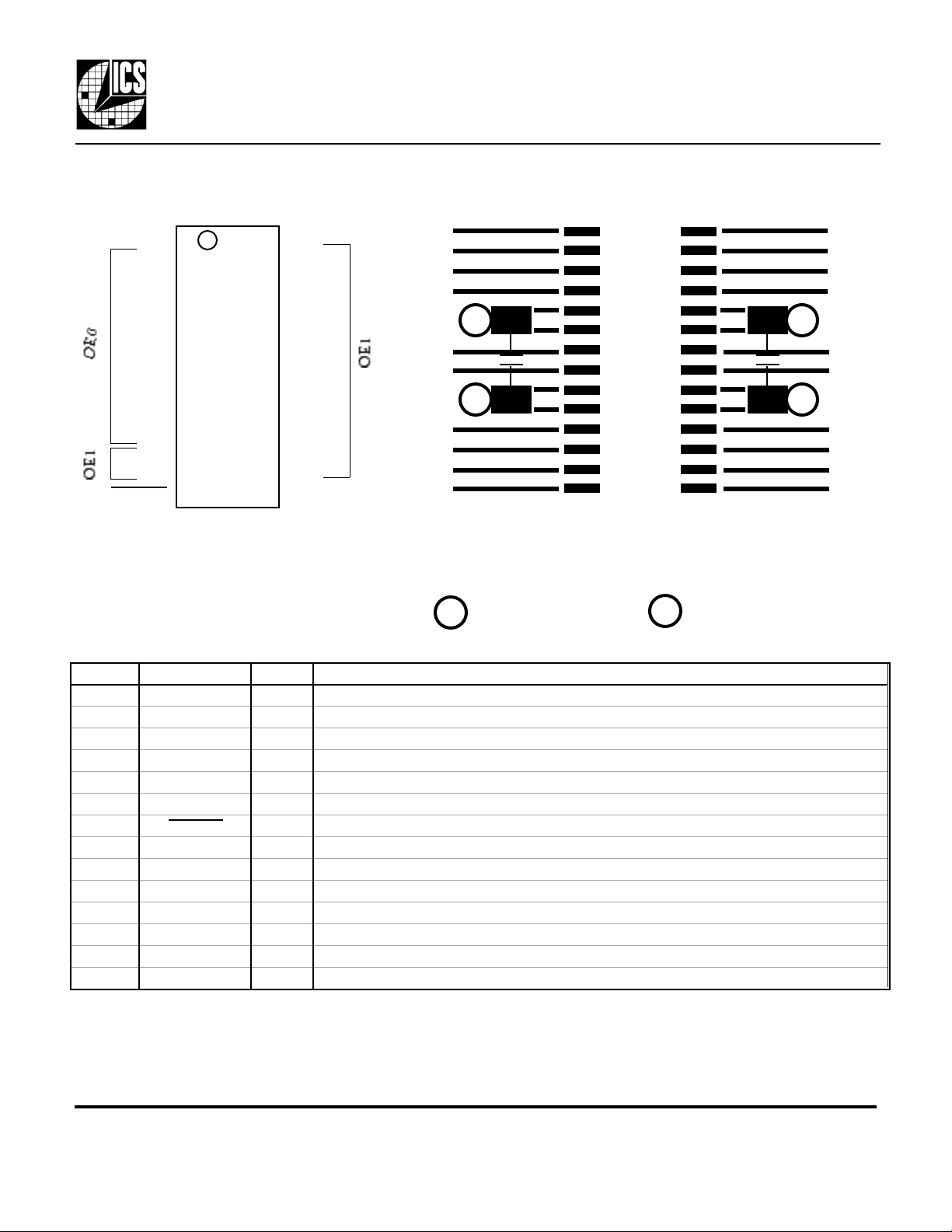
Pin Assignment
1
OE0
2
Q0
Q1
3
Q2
4
5
VDD
VDD
6
Q3
7
Q4
8
Q5
Q6
Q7
9
10
11
12
13
14
GND
GND
PECLIN
28
27
26
25
24
23
22
21
20
19
18
17
16
15
OE1
Q15
Q14
Q13
VDD
VDD
Q12
Q11
GND
GND
Q10
Q9
Q8
PECLIN
Suggested Layout
V
0.1µF
G G
For simplicity, 33 Ω series termination resistors are not
shown for the outputs, but should be placed as close to the
device as possible. It is most critical to have the 0.1µF
decoupling capacitors closest.
= connect to VDD
V
= connect to GNDG
V
0.1µF
Pin Descriptions
Number Name Type Description
1 OE0 I Output Enable. Tri-states Q0 to Q5 clock outputs when this input is low. Internal pull-up.
2, 3, 4 Q0, Q1, Q2 O Clock outputs.
5, 6 VDD P Power supply. Connect to +3.3V.
7, 8 Q3, Q4 O Clock outputs.
9, 10 GND P Connect to ground.
11, 12, 13 Q5, Q6, Q7 O Clock outputs.
14 PECLIN I Complementary PECL input.
15 PECLIN I True PECL input.
16, 17, 18 Q8, Q9, Q10 O Clock outputs.
19, 20 GND P Connect to ground.
21, 22 Q11, Q12 O Clock outputs.
23, 24 VDD P Power supply. Connect to +3.3V.
25, 26, 27 Q13, Q14, Q15 O Clock outputs.
28 OE1 I Output Enable. Tri-states Q6 to Q15 clock outputs when this input is low. Internal pull-up.
Type: I = Input, O = output, P = power supply connection
MDS 74CB163 A 2 Revision 112399
Integrated Circuit Systems, Inc. • 525 Race Street • San Jose •CA•95126• (408)295-9800tel • www.icst.com
 Loading...