ICST MK74CB115RTR, MK74CB115R Datasheet

MK74CB115
1 to 16 Buffalo™ Clock Driver
Description
The MK74CB115 Buffalo™ is a monolithic
CMOS high speed clock driver. It consists of a
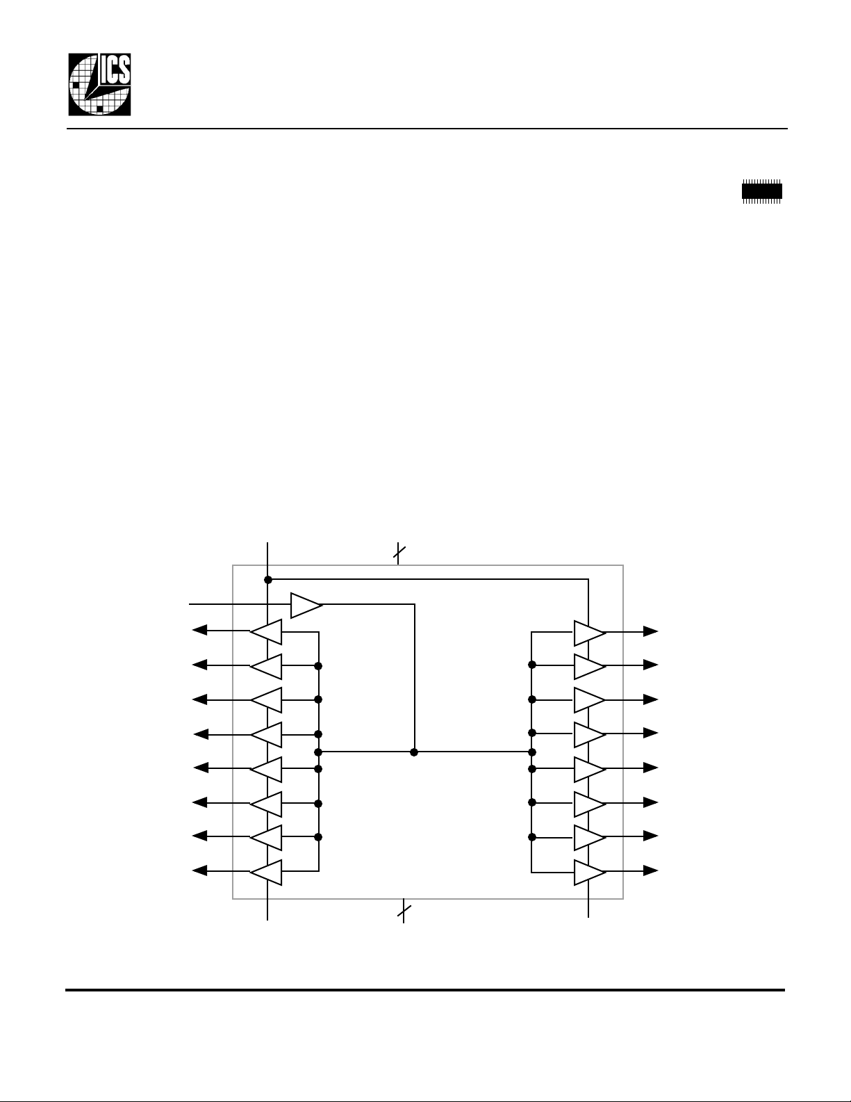
single input to sixteen low-skew output, noninverting clock drivers. The chip is capable of
driving 16 CMOS loads up to 200 MHz with a
maximum of 250 ps output to output skew. The
MK74CB115 is packaged in the tiny 28 pin SSOP,
which uses the same board space as the narrow 16
pin SOIC.
Family of ICS Parts
The MK74CB115 Buffalo™ is designed to be
used with ICS’s clock synthesizer devices. The
inputs of the Buffalo are matched to the outputs of
ICS clock synthesizers. Consult ICS for
applications support.
Block Diagram
OE2
VDD
4
Features
• Tiny 28 pin SSOP (150 mil) package
• One input to sixteen output clock drivers
• Outputs are skew matched to within 250 ps
• 3.3V±10% or 5V±10% supply voltage
• 3 Output Enables allow configuration as 1 to 4,
1 to 6, 1 to 10, 1 to 12 or 1 to 16 buffer
• Clock speeds up to 200 MHz
IN
Q0
Q1
Q2
Q3
Q4
Q5
Q6
Q7
4
OE1
MDS 74CB115 D 1 Revision 020800 Printed 11/16/00
Integrated Circuit Systems, Inc. • 525 Race St. • San Jose • CA • 95126 • (408) 295-9800tel • www.icst.com
GND
OE0
Q15
Q14
Q13
Q12
Q11
Q10
Q9
Q8

MK74CB115
1 to 16 Buffalo™ Clock Driver
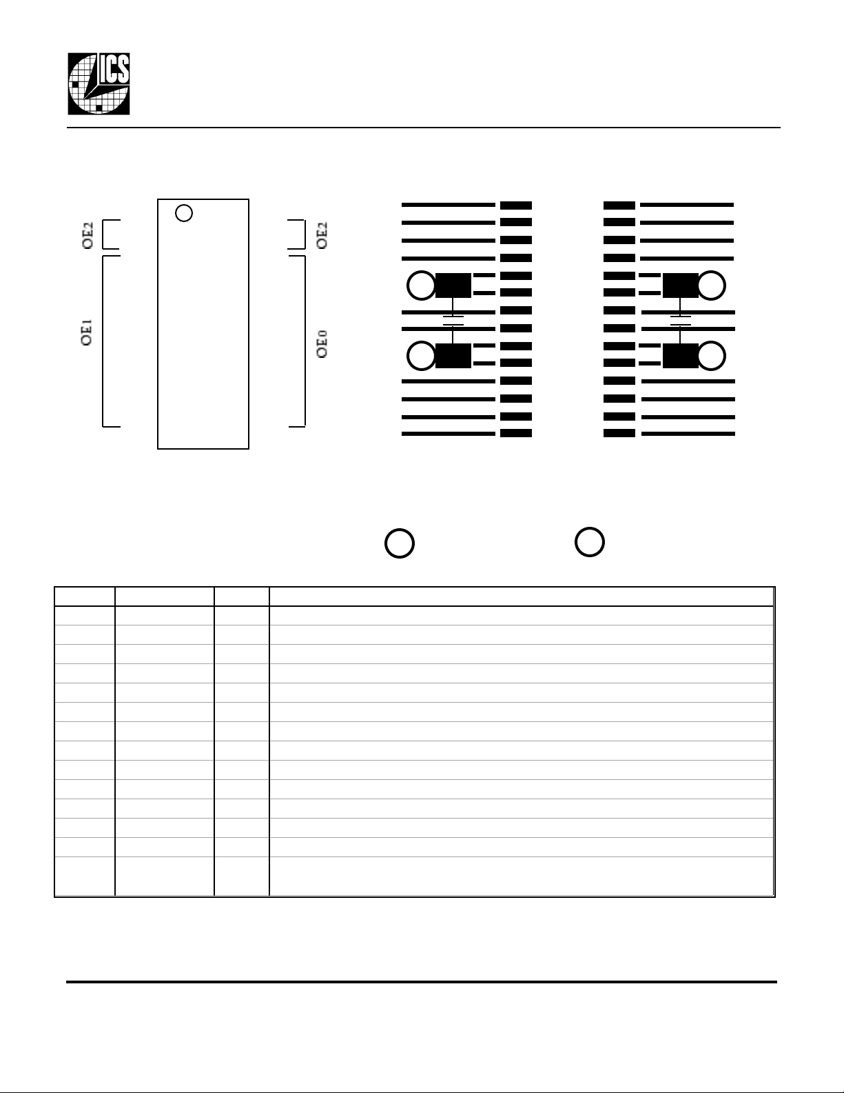
Pin Assignment
1
OE1
2
Q0
Q1
3
Q2
4
5
VDD
VDD
6
Q3
7
8
Q4
Q5
Q6
Q7
IN
9
10
11
12
13
14
GND
GND
28
27
26
25
24
23
22
21
20
19
18
17
16
15
OE2
Q15
Q14
Q13
VDD
VDD
Q12
Q11
GND
GND
Q10
Q9
Q8
OE0
Suggested Layout
V
0.1µF
G
For simplicity, series terminating resistors (required) are
not shown for the outputs, but should be placed as close to
the device as possible. It is most critical to have the 0.1µF
decoupling capacitors closest.
= connect to VDD
V
= connect to GND
G
G
V
0.1µF
Pin Descriptions
Number Name Type Description
1 OE1 I Output Enable. Tri-states Q2 to Q7 clock outputs when this input is low. Internal pull-up.
2, 3 Q0, Q1 O Clock outputs.
4, 7, 8 Q2, Q3, Q4 O Clock outputs.
5, 6 VDD P Power supply. Connect to +3.3 V or 5 V.
9, 10 GND P Connect to ground.
11, 12, 13 Q5, Q6, Q7 O Clock outputs.
14 IN I Clock input for 16 buffers.
15 OE0 I Output Enable. Tri-states Q8 to Q13 clock outputs when this input is low. Internal pull-up.
16, 17, 18 Q8, Q9, Q10 O Clock outputs.
19, 20 GND P Connect to ground.
21, 22, 25 Q11, Q12, Q13 O Clock outputs.
23, 24 VDD P Power supply. Connect to +3.3 V or 5 V.
26, 27 Q14, Q15 O Clock outputs.
28
Type: I = Input, O = output, P = power supply connection
OE2 I Output Enable. Tri-states Q0, Q1, Q15 and Q14 clock outputs when this input is low.
Internal pull-up.
MDS 74CB115 D 2 Revision 020800 Printed 11/16/00
Integrated Circuit Systems, Inc. • 525 Race St. • San Jose • CA • 95126 • (408) 295-9800tel • www.icst.com
 Loading...