MK715
Touch Screen Controller
General Description
The MK715 Touch Screen Controller IC provides all the
screen drive, Analog to Digital converter (ADC) and
control circuits to easily interface to 4-wire analog resistive
touch screens. It also includes a general purpose A to D
converter and a clock synthesizer.
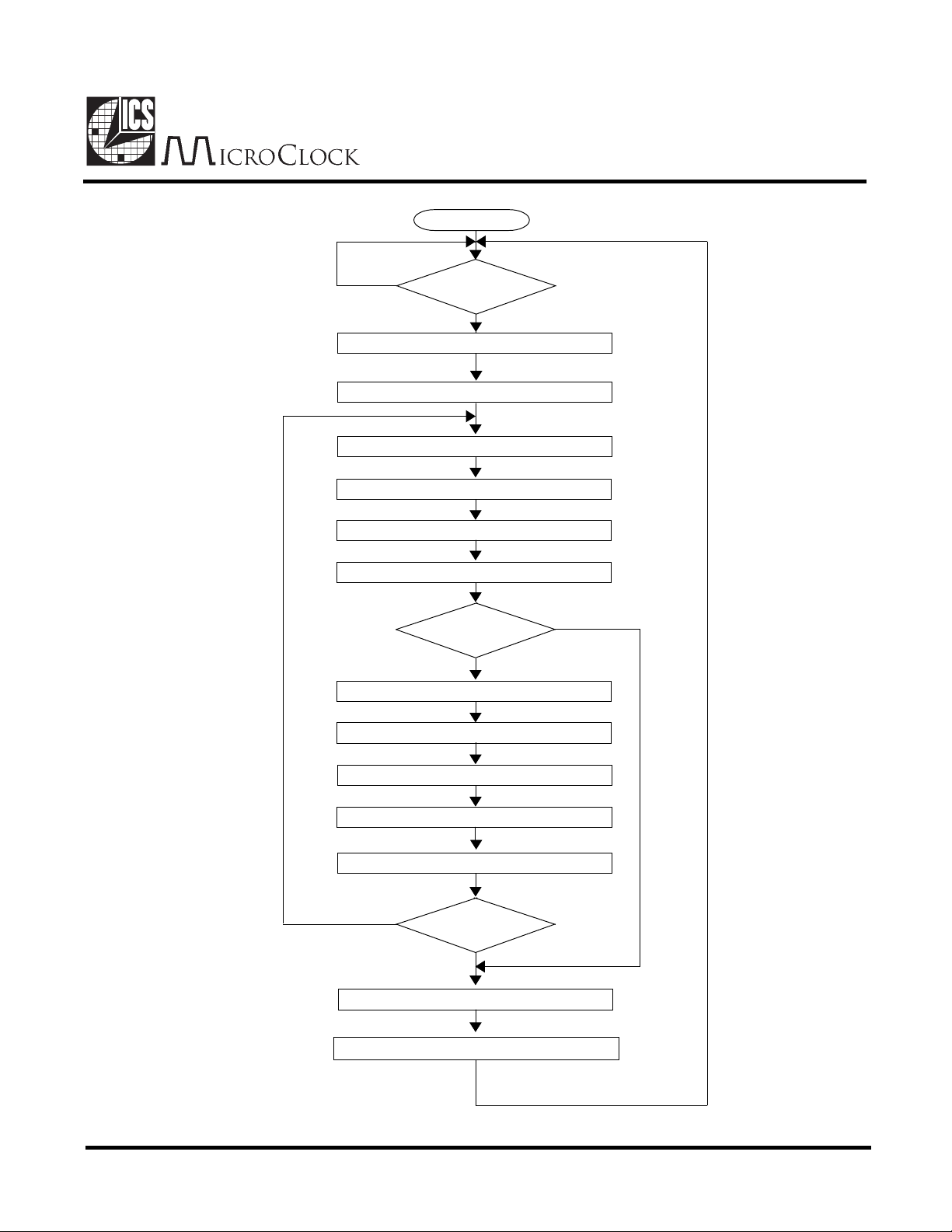
The IC continually monitors the screen waiting for a
touch. In this mode, the supply current is typically 4µA.
When the screen is touched, the IC performs analog to
digital conversions to determine the location of the touch,
stores the X and Y locations in the registers, and issues
an interrupt. This process is repeated up to 303 times per
second until no further screen touches are detected, at
which time the low current mode is resumed.
The device has a general purpose input into the 10-bit
ADC, allowing for the measurement of other inputs such
as battery voltage. The MK715 can be powered from a
3.3V supply, and uses an inexpensive 32.768kHz watch
crystal as the input reference. An internal Phase-Lock
Loop clock synthesizer provides the high speed clock for
the ADC, and the option to have a clock output to drive
other digital chips in the system.
The tiny package is the same body size as the 14 pin
SOIC, with 25 mil spacings on the leads.
Features
Tiny 20 pin SSOP (150 mil body)
4 microamp standby current
Less than 3mA active current at 3.3V, including
screen drive
Touch pressure can be measured
One or two general purpose A to D inputs
On-chip voltage reference
32.768kHz crystal/clock input
MHz clock outputs available
Operates with four wire touch screens
Ratiometric conversion eliminates screen
calibration
Automatic wake up upon screen touch
Programmable conversion rate to a maximum of
303 points per second
3.3V or 5V supply (2.7V version available)
10 bit A/D converter
Full powerdown control
Touch screen is directly driven - no external
transistors are required
A to D Converter guaranteed monotonic
3 or 4 wire serial interface
Applications
Notebook Computers
Handheld Computers
PDAs
Touch-screen kiosks
MK715RevD020200
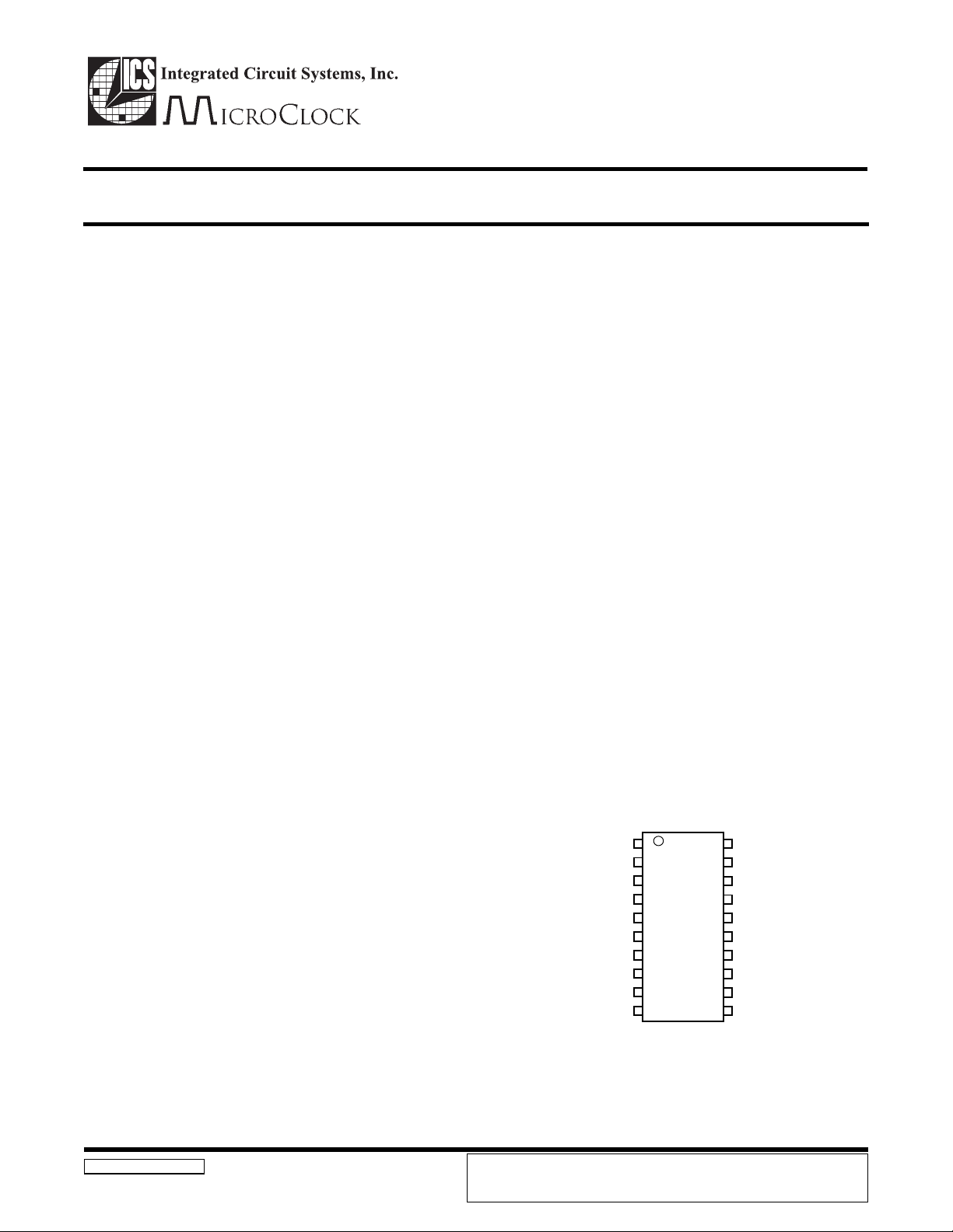
Pin Assignment
CS
SK
1
D0
2
DI
3
TOUCH#
XH
XL
YH
YL
PL
GP
4
5
6
7
8
9
10
MK715
20 pin SSOP
ICS reserves the right to make changes in the device data identified in this publication
without further notice. ICS advises its customers to obtain the latest version of all device
data to verify that any information being relied upon by the customer is current and accurate.
20
19
18
17
16
15
14
13
12
11
CLKOUT
INT
VDD
X2
X1
GND
CAP2
CAP1
CAP3
MK715
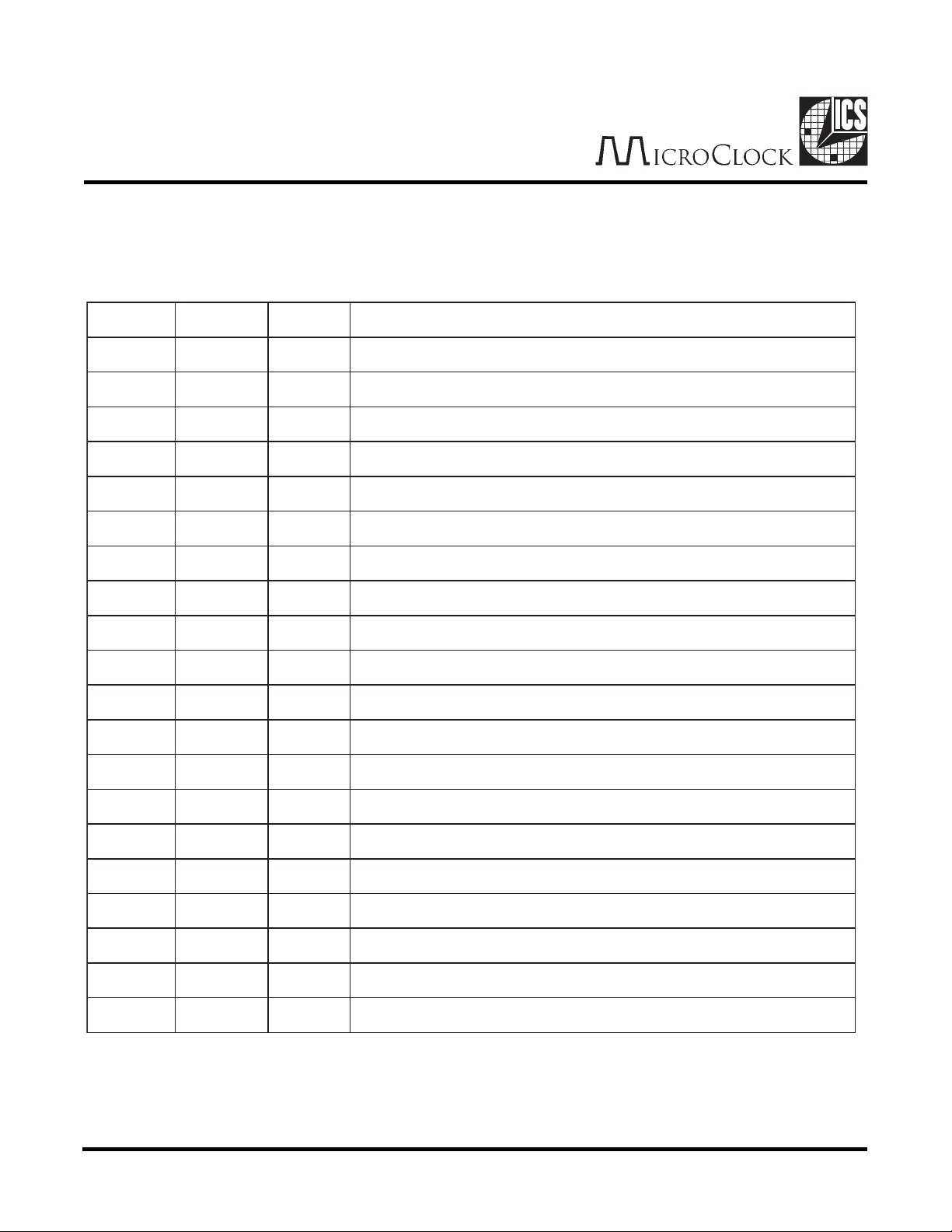
Pin Descriptions
#niPemaNepyTnoitpircseD
1KSI .kcolClaireS
2ODO .3nipottcennoc,troplaireseriw3roF.tuOataD
3IDI .2nipottcennoc,troplaireseriw3roF.nIataD
4#HCUOTO .tuokcolClanoitpO.dehcuotsineercsnehwwolseoG.langiShcuoT
5HXST.)edisthgir(neercshcuotnohgih-XottcennoC
6LXST.)edistfel(neercshcuotnowol-XottcennoC
7HYST.)pot(neercshcuotnohgih-YottcennoC
8LYST.)mottob(neercshcuotnowol-YottcennoC
9LPI .tupniCDAesopruplareneG
01PGI .tupniCDAesopruplareneG
113PAC- .dnuorgotroticapacFu10.0atcennoC
211PAC- .noitcennocretlifpooL
312PAC- .noitcennocretlifpooL
41DNGP .dnuorgottcennoC
511XI .tupnikcolcrofdnuorgro,latsyrczHk867.23ottcennoC
612XI .tupnikcolcrolatsyrczHk867.23ottcennoC
71DDVP .V3.3+roV5+ottcennoC
81TNIO .tuptuokcolclanoitpO.tpurretnilangisothgihseoG.tpurretnI
91TUOKLCO .tuptuozHMeboslanaC.zHk867.23yllacipyT.tuptuokcolC
02SCI .hgihevitcAtcelespihC
Key: I = Input, O = Output, I/O = Input and Output, P = Power, TS = Touch Screen pin.
2

MK715
Chip Overview
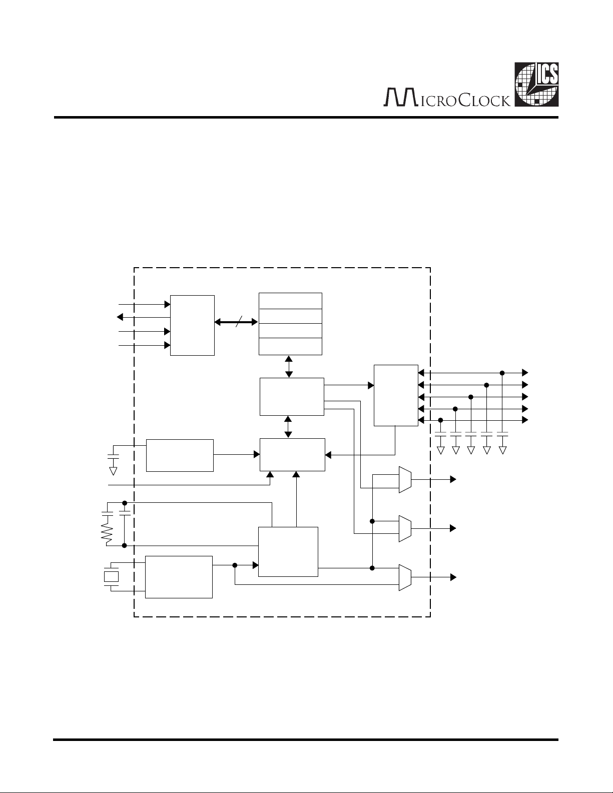
The MK715 communicates via a 4 pin serial port. This may be connected as either a 3 or 4 wire
serial port. The port is connected to 4 registers that control the various modes and function of the
chip.
The primary function of the MK715 is to control resistive touchscreens. There are two ways to read
screen points, both controlled by the registers.
In the first method, which is enabled by setting the ENCONR bit, the MK715 performs periodic
conversions at a rate set by the rate register. The chip monitors the touch screen in a low power
condition (about 4 mA) until the screen is touched. When a touch is detected, the chip powers up
and starts converting screen points. The TOUCH# pin goes low and INT goes high to indicate a
change in touch status. The converter outputs a Y co-ordinate, then an X co-ordinate, then a Y coordinate, and so on. The X and Y co-ordinates are stored in the same register (RESULT) and each
conversion over-writes the previous conversion. When a co-ordinate is stored, the conversion
complete bit is asserted in the STATUS register. This bit is cleared when the RESULT register is
read. The inverted state of the TOUCH# pin also appears in the STATUS register. After each coordinate conversion, INT goes high and the screen is checked to see if it is still touched. If not,
conversions stop, TOUCH# goes high, INT goes high (to indicate a change in touch status) and
the chip reverts to the low power mode.
The second method to read a screen is to set the RD1PT (read one point) bit in the CONTROL
register. The chip will perform two conversions, a Y co-ordinate followed by an X co-ordinate. The
X co-ordinate overwrites the Y co-ordinate and so the X co-ordinate must be read before this
happens. Finally, RD1PT is cleared. The conversion pair takes about 3.5 ms.
The converter may also be used to measure voltages presented on the GP or PL pins. The range
of the converter is 0 to 1.279 V and so voltages outside this range must be scaled appropriately.
Again, the RD1PT bit is set to start the conversion but first either SELGP or SELPL must be set
to select the correct input. Only one conversion is performed. The result is stored in the RESULT
register and then RD1PT is cleared. The conversion takes about 1.7ms.
The final conversion mode is used to measure touch pressure. This is controlled identically to the
second method outlined above except that either RDPRESA or RDPRESB must first be set.
The MK715 allows for several different clocks to be generated, controlled by the registers. On the
CLKOUT pin, the output is either a a 32768 Hz clock from the crystal oscillator or a MHz - frequency
clock synthesized from the PLL. Similarly, this MHz - frequency clock can appear on the INT or
TOUCH# pins instead of their usual functions. In these cases, if the MHz clock needs to run
continuously, then the ENPLL bit must be set in order to override the automatic powerdown of the PLL.
Refer to page 12 for more details.
3
MK715
Block Diagram
Registers
CAP3
GP
CAP1
CAP2
DI
D0
CS
SK
X1
X2
Serial
Port
Voltage
Reference
32.768kHz
Oscillator
12
Status
Rate
Result
Control
Controller
10 Bit A-D
Converter
Phase
Locked
Loop
0
1
2
3
XH
Screen
Drive
1
0
1
0
1
0
INT
TOUCH#
CLKOUT
XL
YH
YL
PL
4
MK715
IC Operation
(Periodic Conversions Enabled)
Power ON
N
Is screen
touched?
Y
Write D6 Reg 0 to 1 and TOUCH# = 0
Issue Interrupt, power-up ADC and PLL
Convert Y co-ordinates
Store Y co-ordinates in Register 2
Write D7 register 0 to 1
Issue interrupt
Is screen
touched?
N
Y
Convert X co-ordinates
Store X co-ordinates in Register 2
Write D7 register 0 to 1
Issue Interrupt
Wait. Duration controlled by Rate Register
Y
Is screen
touched?
N
Write D6 Reg 0 to 0 and TOUCH# = 1
Issue Interrupt, power-down ADC and PLL
5
MK715
Register Description
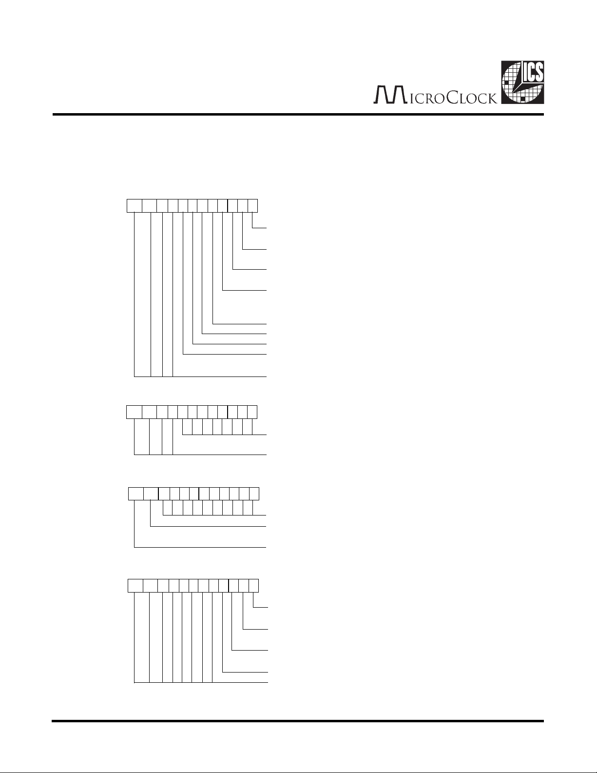
The MK715 has four 12 bit registers. However, only 8 bits in each register can be written (D0-D7). The other 4 bits (D8D11) can never be written and are always read only.The RESULT register contains 2 levels, a read only level and a write
only level. Reading this register gives the conversion results. Writing this register changes 4 control bits.
DESCRIPTION
Read
and
Write
Read
and
Write
STATUS (ADDRESS 0)
11 10 9 8 7 6 5 34210
RATE (ADDRESS 1)
11 10 9 8 7 6 5 34210
RD1PT. Read one point. Cleared when
conversion complete.
ENCONR. Enable periodic screen conversions
at rate set by RATE register.
PD. Power Down. Chip powers down. See
CONTROL register bit 7.
ENPLL. Overrides automatic powerdown of
PLL between conversions and forces
continuous running.
SELGP. Select GP input to ADC.
SELPL. Select PL input to ADC.
Touch Status. 1 = touch.
Conversion complete. Cleared on next read
of RESULT register.
Always set to zero.
Controls frequency of screen conversions
when periodic conversions are enabled.
Always set to zero.
TYPE
R/W
R/W
R/W
R/W
R/W
R/W
RO
RO
RO
R/W
RO
Power-up
State
0
0
0
0
0
0
0
0
0
32
0
Read
Write
RESULT (ADDRESS 2)
11 10 9 8 7 6 5 34210
RESULT (ADDRESS 2)
11 10 9 8 7 6 5 34210
10-bit conversion result.
XSEL. Screen conversion status. 0 = Y
coordinate, 1 = X coordinate.
Conversion type. 0 = non-screen
conversion, 1 = screen conversion.
RDPRESA. Read pressure A. See
description of measuring touch pressure.
RDPRESB. Read pressure B. See
description of measuring touch pressure.
PLZERO. Forces PL pin to ground. Can be
used to control an external resistor divider.
Test mode. ALWAYS WRITE TO 0.
Don't Care.
6
RO
RO
RO
WO
WO
WO
WO
-
X
0
1
0
0
0
0
X
Register Description (cont.)
MK715
DESCRIPTION
Read
CONTROL (ADDRESS 3)
11 10 9 8 7 6 5 34210
and
Write
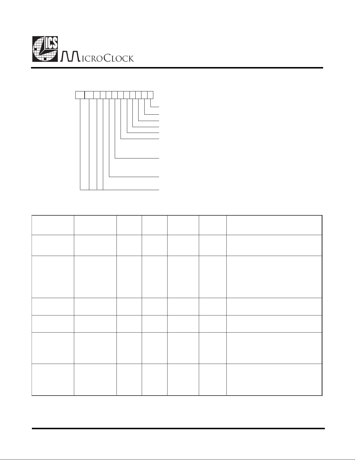
SEL0. Clock select 0. See page 11.
SEL1. Clock select 1. See page 11.
SEL2. Clock select 2. See page 11.
SEL3. Clock select 3. See page 11.
SEL4. Clock select 4. See page 11.
CLKSEL. Clock frequency select.
See page 11. 0 = 14.3196 MHz
1 = 14.7456 MHz
Set to 0.
DIS32. Determines state of 32.768 kHz
oscillator when PD asserted (STATUS register).
Always set to zero.
R/W = Read/Write, RO = Read Only, WO = Write Only
Converter Control
BSERPDRASERPDRLPLESPGLESRNOCNETP1DRDEMROFREPNOISREVNOC
000001ot0
000010
TYPE
R/W
R/W
R/W
R/W
R/W
R/W
R/W
R/W
RO
Power-up
State
0
0
0
0
0
0
0
0
0
ehtnosnoisrevnoc2smrofreP
XnanehtdnaYa-neercs
.deraelcnehtsiTP1PR.noisrevnoc
tessaetartasnoisrevnocelbanE
sineercsnehW.retsigerETARni
setareporetrevnoc,dehcuot
sihcuotonlitnuylsuonitnoc
yllacitamotuanehtpihC.detceted
.etatsybdnats,rewopwolotseog
000101ot0
001001ot0
010001ot0
.deraelc
100001ot0
.deraelc
PGnonoisrevnocenosmrofreP
.deraelcsiTP1DR.tupni
LPnonoisrevnocenosmrofreP
.deraelcsiTP1DR.tupni
dnaYa,snoisrevnocowtsmrofreP
erusserphcuotevigot,Xnaneht
hcuotnonoitceseeS.atad
siTP1DR.tnemerusaemerusserp
dnaYa,snoisrevnocowtsmrofreP
erusserphcuotevigot,Xnaneht
hcuotnonoitceseeS.atad
siTP1DR.tnemerusaemerusserp
The converter must be sequenced correctly - before writing RD1PT to one, the appropriate bit (e.g. SELGP) must
first be set in a previous write. Only the combinations shown above are permitted. Other combinations will give
unpredictable behavior.
7
 Loading...