MK3721
Revision 082800
Integrated Circuit Systems, Inc. • 525 Race Street • San Jose •CA • 95126• (408)295-9800tel • www.icst.com
ICRO
C
LOCK
Description
The MK3721 is ICS/MicroClock’s lowest cost,
low jitter, high performance 3.3 volt VCXO
designed to replace expensive VCXO modules.
The on-chip Voltage Controlled Crystal Oscillator
accepts a 0 to 3.3 V input voltage to cause the
output clocks to vary by ±100 ppm. Using
ICS/MicroClock’s patented VCXO techniques,
the device uses an inexpensive external pullable
crystal in the range of 16.2 - 28 MHz to produce a
VCXO output clock at that same frequency.
ICS/MicroClock manufactures the largest variety
of Set-Top Box and multimedia clock synthesizers
for all applications. If more clock outputs are
needed, see the MK3732 or MK377x family of
parts. Consult ICS/MicroClock to eliminate
VCXOs, crystals and oscillators from your board.
Low Cost 3.3 Volt VCXO
Features
• Packaged in 8 pin SOIC
• 3.3 V operating voltage
• 16.2 MHz to 28 MHz operation
• Uses an inexpensive external crystal
• On-chip VCXO (patented) with pull range of
200 ppm (minimum)
• VCXO tuning voltage of 0 to 3.3 V
• 12 mA output drive capability at TTL levels
• Advanced, low power, sub-micron CMOS process
• For frequencies between 8 MHz to 16 MHz, use
the MK3711A. For frequencies between 1 MHz
and 8 MHz, use the MK3713. For higher than
28 MHz, use the MK3732-05
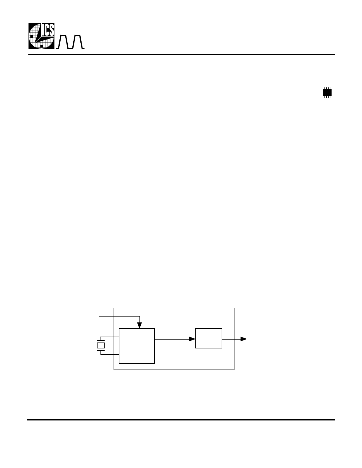
Block Diagram
VIN
X1
16.2 -28 MHz
pullable crystal
X2
MDS 3721 B 1
Voltage
Controlled
Crystal
Oscillator
Output
Buffer
16.2 - 28 MHz Clock
(REFOUT)

MK3721
Revision 082800
Integrated Circuit Systems, Inc. • 525 Race Street • San Jose •CA • 95126• (408)295-9800tel • www.icst.com
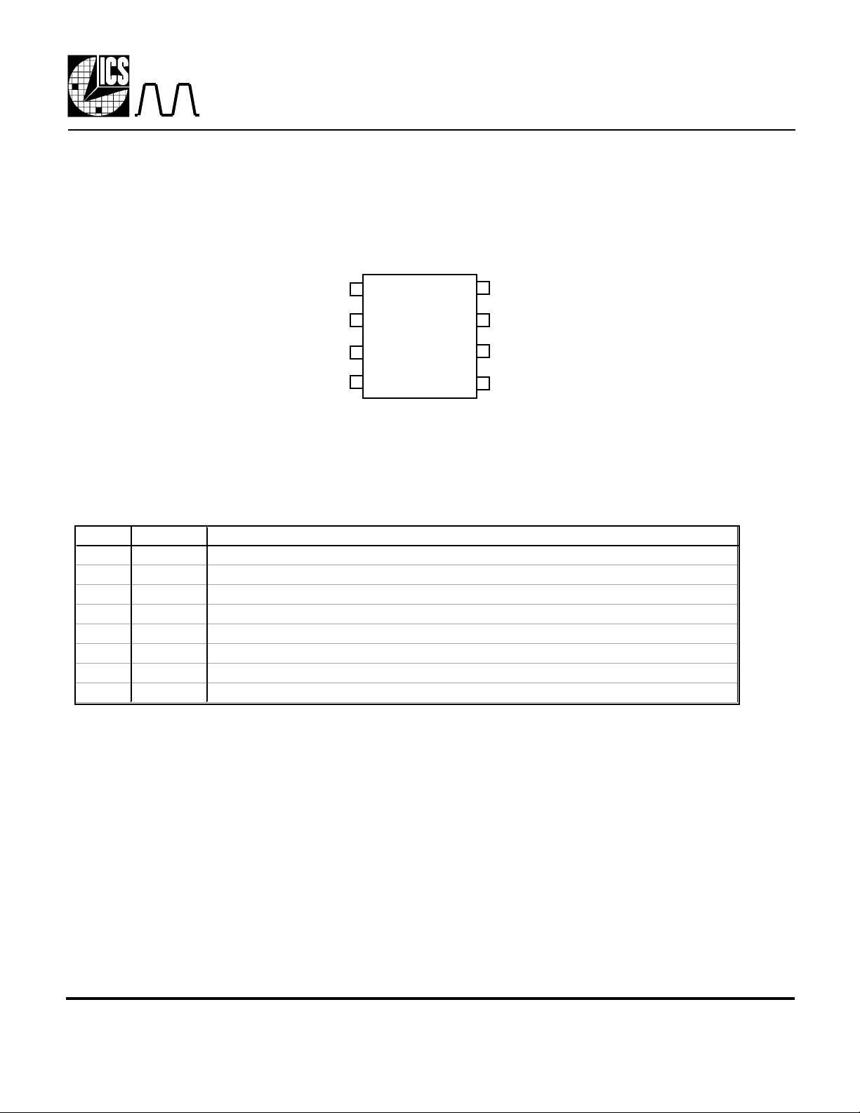
Pin Assignment
Pin Descriptions
ICR O
C
LOCK
VDD
VIN
GND
Low Cost 3.3 Volt VCXO
MK3721
X1
1 8
2
3
4
7
6
5
8 pin (150 mil) SOIC
X2
DC
REFOUT (VCXO)
DC
Number Name Description
1 X1 Crystal connection. Connect to a pullable 16.2 - 28 MHz crystal.
2 VDD VDD. Connect to + 3.3 V.
3 VIN Voltage input to VCXO. Zero to 3.3 V analog input which controls the frequency of the VCXO.
4 GND Connect to ground.
5 DC Don't Connect anything to this pin.
6 REFOUT VCXO CMOS level clock output matches the nominal frequency of the crystal.
7 DC Don't Connect anything to this pin.
8 X2 Crystal connection. Connect to a pullable 16.2 - 28 MHz crystal.
Crystal Specifications
Correlation (load) capacitance 14 pF
Initial accuracy ±20 ppm maximum
Drift over temperature and aging ±50 ppm maximum
C0/C1 ratio 240 maximum
ESR 35 Ω maximum
MDS 3721 B 2
 Loading...