

ICST MK3720STR, MK3720A, MK3720ATR, MK3720S Datasheet
MK3720
27 MHz and 54 MHz 3.3 Volt VCXO
Description
The MK3720 is a low cost, low jitter, high
performance 3.3 Volt VCXO and PLL clock
synthesizer designed to replace expensive 13.5, 27,
or 54MHz VCXOs. The patented on-chip
Voltage Controlled Crystal Oscillator accepts a
0 to 3.3 V input voltage to cause the output clocks
to vary by ±100 ppm. Using our patented VCXO
and analog/digital Phase-Locked Loop (PLL)
techniques, the device uses an inexpensive external
13.5 MHz pullable crystal input to produce output
clocks of 13.5 MHz, 27 MHz, and 54 MHz .
The MK3720A is a drop-in replacement to the
earlier MK3720S.
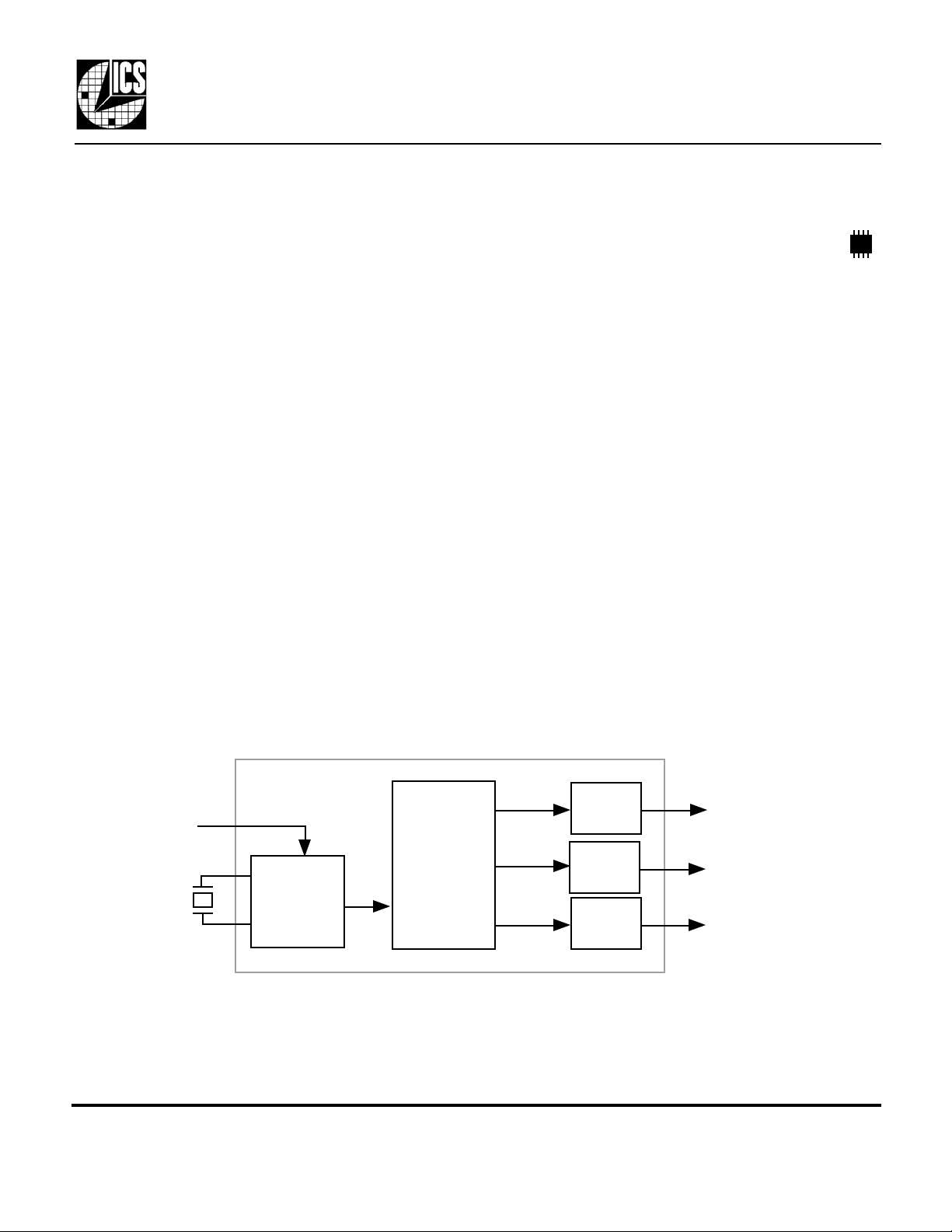
Block Diagram
Features
• Packaged in 8 pin SOIC
• 3.3 V only operating voltage
• Output clocks of 54, 27, and 13.5MHz
• Uses an inexpensive 13.500 MHz external crystal
• On-chip patented VCXO with pull range
of 200ppm (minimum)
• VCXO tuning voltage of 0 to 3.3 V
• 12 mA output drive capability at TTL levels
• Advanced, low power, sub-micron CMOS process
• The A version is the latest, manufactured in a smaller
geometry process. The MK3720A gives a wider pull
range than the MK3720S, and so is recommended
for all new designs, and cost reductions of existing
designs.
Output
VIN
13.5 MHz
pullable
crystal
MDS 3720 D 1 Revision 053100 Printed 11/16/00
Integrated Circuit Systems, Inc. •525 Race Street • San Jose • CA• 95126• (408)295-9800tel • www.icst.com
X1
X2
Voltage
Controlled
Crystal
Oscillator
PLL/Clock
Synthesis
Circuitry
Buffer
Output
Buffer
Output
Buffer
54 MHz Clock
27 MHz Clock
13.5 MHz Clock
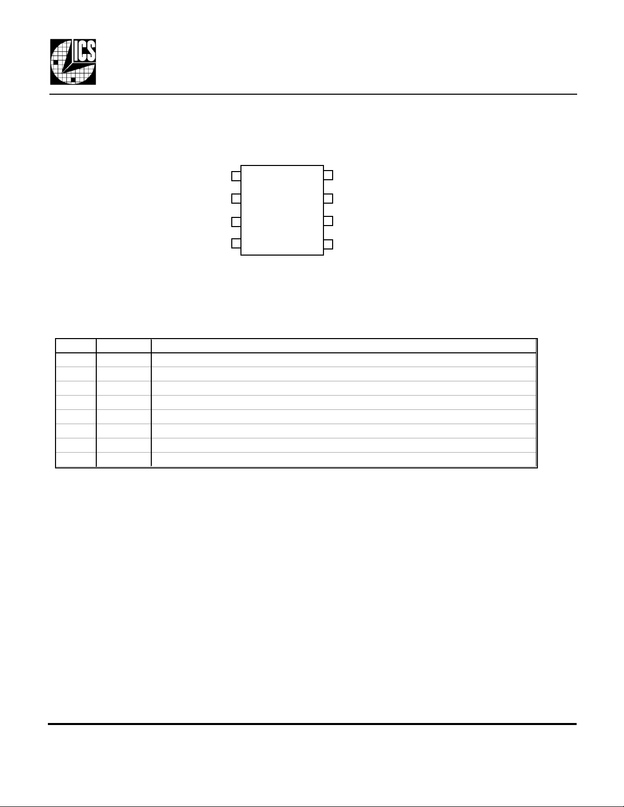
Pin Assignment
MK3720
27 MHz and 54 MHz 3.3 Volt VCXO
MK3720
X1
VDD 27M
VIN
GND
1 8
2
3
4
X2
7
6
13.5M
5
54M
8 pin (150 mil) SOIC
Pin Descriptions
Number Name Description
1 X1 Crystal connection. Connect to a pullable 13.5 MHz crystal.
2 VDD VDD. Connect to +3.3 V.
3 VIN Voltage input to VCXO. Zero to 3.3 V analog input which controls the frequency of the VCXO.
4 GND Connect to ground.
5 54M 54 MHz VCXO clock output.
6 13.5M 13.5 MHz VCXO clock output.
7 27M 27 MHz VCXO clock output.
8 X2 Crystal connection. Connect to a pullable 13.5 MHz crystal.
Pullable Crystal Specifications:
Correlation (load) Capacitance 14 pF
C0/C1 240 max
ESR 35 Ω max
Operating Temperature 0 to 70 °C
Initial Accuracy ±20 ppm
Temperature plus Aging Stability ±50 ppm
MDS 3720 D 2 Revision 053100 Printed 11/16/00
Integrated Circuit Systems, Inc. •525 Race Street • San Jose • CA• 95126• (408)295-9800tel • www.icst.com
 Loading...