ICST MK3711S, MK3711BTR, MK3711D, MK3711ATR, MK3711STR Datasheet
...
MK3711
LOW COST 8 - 16 MHZ 3.3 VOLT VCXO
Description
The MK3711 series of devices include the original
MK3711S, MK3711A, and the new MK3711B and
MK3711D. The MK3711D and MK3711B are drop-in
replacements for the MK371 1S and MK371 1A devices.
Compared to these earlier devices the MK3711D and
MK3711B offer a wider operating frequency range and
improved power supply noise rejection.
The MK3711 series combines the functions of a VCXO
(Voltage Controlled Crystal Oscillator) and PLL (Phase
Locked Loop) frequency doubler onto a single chip.
Used in conjunction with an external pullable quartz
crystal, this monolithic integrated circuit replaces more
costly hybrid (canned) VCXO devices. The MK3711 is
designed primarily for data and clock recovery
applications within end products such as ADSL
modems, set-top box receivers, and telecom systems.
The MK3711D exhibits a moderate VCXO gain of
120ppm/V typical, when used with a high quality
external pullable quartz crystal. The MK3711B offers a
higher VCXO gain of 150ppm/V, similar to the earlier
MK3711A. The higher intrinsic VCXO gain of the
MK3711C may help compensate for the reduced
pullability of a low quality crystal used in some
applications. However, higher VCXO gain may also
increase clock output phase noise.
The frequency of the on-chip VCXO is adjusted by an
external co ntrol volt ag e inpu t in to pi n VI N. Si nce VIN is
a high impedance input, it can be driven directly from
an PWM RC integrator circuit. Frequency output
increases with VIN voltage input. The usable range of
VIN is 0 to 3V.
Features
• MK3711D and MK3711B are drop-in replacements
for the earlier MK3711S and MK3711A devices
• MK3711D and MK3711B offer 24-36 MHz output
frequency range (output frequency = 2x crystal
frequency) and improved power supply noise
rejection
• Uses an inexpensive 12 to 18 MHz external crystal
• Ideal for ADSL application s usi ng 17.664 MHz
external pullable crystal to generate locked 35.328
MHz clock physical layer clock
• Ideal for set-top box applications using 13.5 MHz
external pullable crystal to generate lock 27 MHz
clock transport video clock
• On-chip VCXO with guaranteed pull range of ±115
ppm minimum (MK3711D)
• VCXO tuning voltage 0 to 3.3 V
• Packaged in 8 pin SOIC (150 mil wide)
MK3711D is Recommended for New Designs
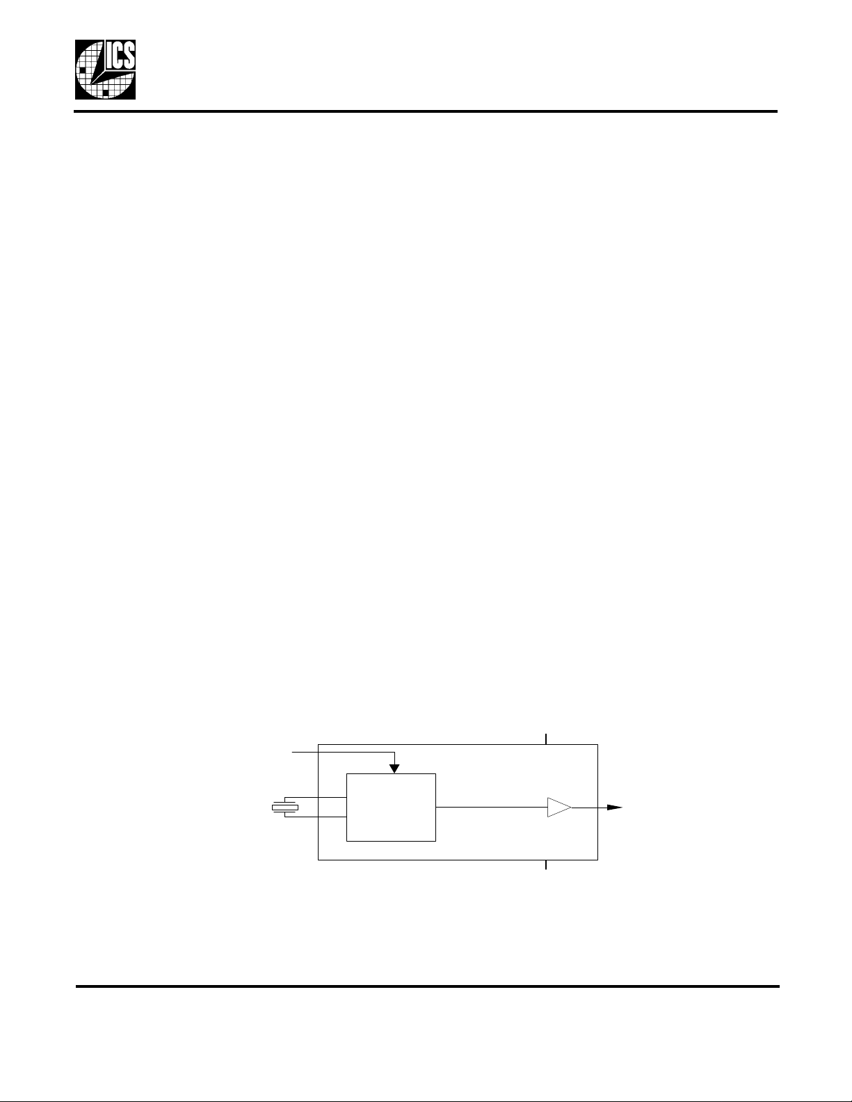
Block Diagram
VDD
VIN
8-1 6 M Hz
P ulla b le
C rystal
MDS 371 1 F 1 Revision 070301
Integrated Circuit Systems ● 525 Race Street, San Jose, CA 95 126 ● tel (408) 295-9800 ● www.icst.com
X1
X2
Voltage
Controlled
C rystal
O scilla to r
8-16 M Hz
GND

Pin Assignment
X1
VDD
VIN
DC
GND
REF
DC
X21
2
3
4
8
7
6
5
MK3711S
MK3711A
MK3711B
MK3711D
8 Pin (150 mil) SOIC
MK3711
LOW COST 8 - 16 MHZ 3.3 VOLT VCXO
Pin Descriptions
Pin
Number
1 XI Input Crystal connection. Connect to the external pullable crystal.
2 VDD Power Connect to +3.3 V (0.01uf decoupling capacitor recommended).
3 VIN Input Voltage input to VCXO -- 0 to 3.3 V analog input which controls the
4 GND Power Connect to ground.
5 DC -- Do not connect anything to this pin.
6 REF Output VCXO CMOS level clock output matches the nominal frequency of the
7 DC -- Do not connect anything to this pin.
8 X2 Input Crystal connection. Connect to the external pullable crystal.
Pin
Name
Pin
Type
Pin Description
oscillation frequency of the VCXO.
crystal.
MDS 3711 F 2 Revision 070301
Integrated Circuit Systems ● 525 Race Street, San Jose, CA 95126 ● tel (408) 295-9800 ● www.icst.com
 Loading...